Spin-valley-coupled quantum spin Hall insulator with topological Rashba-splitting edge states in Janus monolayer
Abstract
Achieving combination of spin and valley polarized states with topological insulating phase is pregnant to promote the fantastic integration of topological physics, spintronics and valleytronics. In this work, a spin-valley-coupled quantum spin Hall insulator (svc-QSHI) is predicted in Janus monolayer with dynamic, mechanical and thermal stabilities. The inequivalent valleys have opposite Berry curvature and spin moment, which can produce a spin-valley Hall effect. In the center of Brillouin zone, a Rashba-type spin splitting can be observed due to missing horizontal mirror symmetry. Moreover, monolayer shows unique Rashba-splitting edge states. Both energy band gap and spin-splitting at the valley point are larger than the thermal energy of room temperature (25 meV) with generalized gradient approximation (GGA) level, which is very important at room temperature for device applications. It is proved that the spin-valley-coupling and nontrivial quantum spin Hall (QSH) state are robust again biaxial strain. Our work may provide a new platform to achieve integration of topological physics, spintronics and valleytronics.
I Introduction
Since the valley-dependent effects are discovered in monolayer with missing inversion symmetry, the field of valleytronics is truly flourishingq1 ; q2 ; q3 . For hexagonal two-dimensional (2D) materials like monolayer , the conically shaped valleys at -K and K corners are inequivalent, and the spin polarizations are opposite, as the two points are connected by the time reversal symmetry operation. The combination of inversion symmetry breaking and spin-orbit coupling (SOC) can remove spin degeneracy, and then gives rise to valley-contrasting spin splitting, which is the foundation for spin-valleytronics. With an applied in-plane electric field, the charge carriers with opposite valley and spin indexes will attain opposite anomalous transverse velocity, and then a simultaneous spin and valley Hall effect is producedq4 ; q5 ; q5-1 .
On the other hand, the topological insulator (TI) has spin-momentum-locked conducting edge states and insulating properties in the bulk, whose charge and spin transport in the edge states are quantized dissipationlesst1 ; t2 . These bring possibilities for low-dissipation electronic devices. For 2D materials, the TI is also called as QSH insulator (QSHI) characterized by counter-propagating edge currents with opposite spin polarization, which is firstly predicted in graphenet3 . Experimentally confirmed QSHIs include the HgTe/CdTe and InAs/GaSb quantum wellst4 ; t5 , and many other 2D materials have been proposed as QSHIs by the first-principles calculationst6 ; t7 ; qt3 ; t8 ; t9 ; t10 . To this end, it’s a natural idea to achieve the integration of QSHI with spin-valleytronics (namely, svc-QSHI).
Several type atomic sheets have been experimentally synthesized, for example nanosheetsq6 . Recently, 2D monolayers have also been theoretically reportedq7 ; q8 ; q9 ; q10 . The monolayer can be used as anode for sodium-ion batteriesq7 , and the massless Dirac-Fermions can be achieved in monolayerq8 . In addition to this, the QSHIs and topological Rashba-splitting edge states in monolayer (X=Sb and Bi) with inversion symmetry have been predictedq10 . The with 1T’ phase is a QSHI, and the corresponding Janus structures MoSSe can still possess nontrivial topology tuned by straingsd4-1 . Compared to , the MoSSe will lose inversion symmetry. Inspiring from this, we construct Janus monolayer based on monolayer (X=Sb and Bi). By first principles simulations, we show that Janus monolayer is a svc-QSHI with topological Rashba-splitting edge states. Calculated results show these novel features are robust again biaxial strain. These results make monolayer an appealing original quantum material for topological physics, spintronics and valleytronics.
| 7.772 | 2.131 | 2.217 | 115.442 | 115.154 | 1.901 |
| / | |||||
| 26.01 | 9.13 | 8.44 | 22.81 | 0.351 |
II Computational detail
Within density functional theory (DFT)1 , we perform the first-principles calculations using the projected augmented wave (PAW) method, as implemented in the VASP packagepv1 ; pv2 ; pv3 . We use GGA of Perdew, Burke and Ernzerhof (GGA-PBE)pbe as the exchange-correlation potential. The cutoff energy for plane-wave expansion is 500 eV with the total energy convergence criterion being eV. To avoid interactions between two neighboring images, the vacuum region along the z direction is set to be larger than 18 . The SOC is incorporated for band structure calculations. The Brillouin zone is sampled by using a 12121 K-point meshes for geometry optimization, elastic coefficients and self-consistent electronic structure calculations. The geometry optimization is considered to be converged, when the residual force on each atom is less than 0.0001 . Phonon dispersion spectrum is attained by the Phonopy codepv5 based on finite displacement method using a 551 supercell. The invariants are used to investigate topological properties of Janus monolayer , as implemented by the Wannier90 and WannierTools codesw1 ; w2 , where a tight-binding Hamiltonian with the maximally localized Wannier functions is fitted to the first-principles band structures. We use PYPROCAR code to obtain the constant energy contour plots of the spin texturepy .
III Crystal and electronic structures
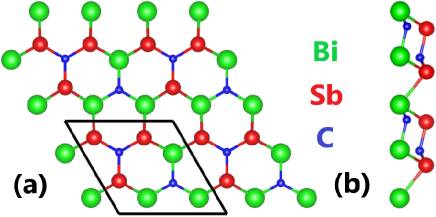
Based on DFT calculations, the optimized lattice parameters of Janus monolayer is 7.772 , which is between ones of (7.58 ) and (7.96 )q10 . As shown in Figure 1 with top and side views, each C atom forms three C-Sb or C-Bi bonds with three neighboring Sb or Bi atoms, and each Sb/Bi atom forms two Sb-Bi bonds and one C-Sb/Bi bond with neighboring Bi/Sb and C atoms, respectively. The symmetry of Janus monolayer with space group (No.156) is lower than that of / monolayer with space group (No.164) due to the lack of space inversion symmetry. Monolayer / is composed of two C atomic layers sandwiched between Sb/Bi atomic layers. Similar to Janus monolayer MoSSe from e1 ; e2 , the Janus monolayer can be constructed by replacing one of two Sb/Bi layers with Bi/Sb atoms in monolayer /. For Janus monolayer , the inequivalent C-Sb and C-Bi bond lengths (Sb-C-Sb and Bi-C-Bi bond angles) will be induced due to the difference in atomic sizes and electronegativities of Sb and Bi atoms, and they are 2.131 and 2.217 (115.442∘ and 115.154∘), which gives rise to a built-in electric field. The symmetry reduce will induce Rashba spin splitting, valley degree of freedom and piezoelectric polarizations.
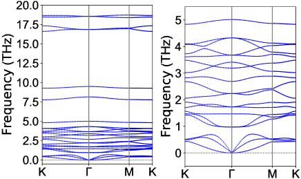
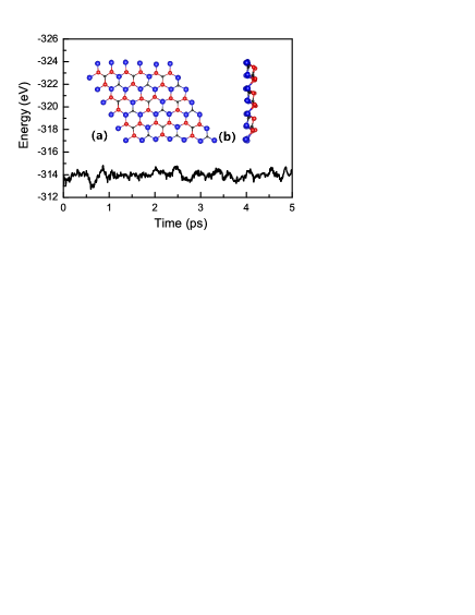
To confirm the stability of Janus monolayer , phonon spectra, ab initio molecular dynamics (AIMD) simulations and elastic constants are carried out. Figure 2 shows that all phonon branches have no imaginary frequency in the entire Brillouin zone, suggesting its dynamical stability. It is noted that two in-plane acoustic branches show linear dispersions, while the ZA branch corresponding to the out-of-plane vibrations displays a quadratic dispersion. These conform to quadratic dispersion of ZA phonon branch, when a 2D material is free of stressr1 ; r2 . The optical branches are well separated from acoustic branches with a gap of 0.29 THz, which prohibits the scattering between acoustic and optical phonon modes. The vibration of the O atoms are mainly at high frequency region. As shown in Figure 3, after heating at 300 K for 5 ps, neither structure reconstruction nor bond breaking with small energy fluctuations for monolayer is observed, suggesting its thermal stability.
Using Voigt notation, the 2D elastic tensor with space group can be reduced into:
| (1) |
The two independent elastic constants of monolayer are =26.01 and =9.13 . The shear modulus equals to , which can be attained by (-)/2, and the corresponding value is 8.44 . The calculated satisfy the Born criteria of mechanical stability of a material with hexagonal symmetryela : and , confirming its mechanical stability. The Young’s modulus can be calculated by the following equationela1 :
| (2) |
where . The monolayer is mechanically isotropic due to hexagonal symmetry, and the is 22.81 , which is obviously smaller than those of other 2D materialsy1 ; y2 ; y3 , suggesting that monolayer is more flexible than other 2D materials. The Poisson’s ratio is also isotropic, and can be simply written as:
| (3) |
The calculated of monolayer is 0.351. The related data are summarized in Table 1.
Next, we provide some suggestions on experimental aspects. Firstly, the / monolayer may be experimentally achieved by the bottom-up approaches such as the molecular beam epitaxy (MBE)q10 , because the epitaxial sheet with a similar structure has been successfully synthesizedq6 . Similar to Janus monolayer MoSSe from e1 ; e2 , the Janus monolayer can be synthesized experimentally with similar experimental techniques based on / monolayer.
IV Electronic structures
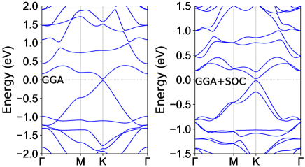
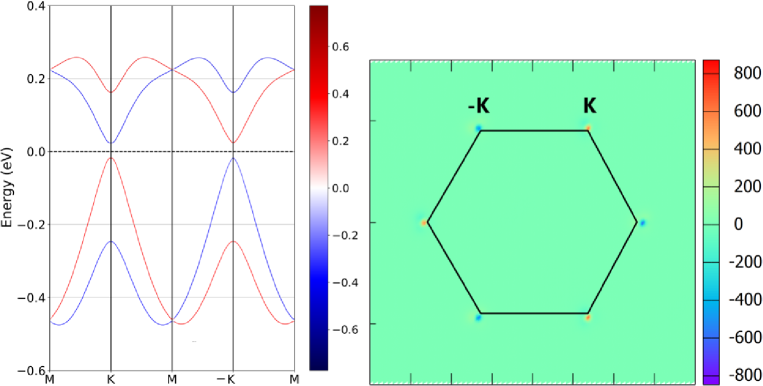
The energy band structures of Janus monolayer with both GGA and GGA+SOC are plotted in Figure 4. In the absence of SOC, one observes that is a direct band-gap semiconductor with both conduction-band minimum (CBM) and valence-band maximum (VBM) at K point with a gap of 39.9 meV. This is different from that of / with gapless Dirac points at K points due to symmetry reduce. Based on the projected band states to atomic orbitals, the states near the band edges are dominated by the C- orbitals and the Sb/Bi- orbitals. When considering SOC, one observes that is still a direct band-gap semiconductor with a gap of 40.1 meV. The main SOC effect is to give rise to a spin splitting of the GGA bands. From the symmetry perspective, the inversion symmetry breaking lifts the spin degeneracy at each generic k point. For /, no spin degeneracy is removed within SOC due to existing inversion symmetryq10 . The spin-splitting at the K point is as large as 139 meV () and 229 meV () for the lowermost conduction band (LCB) and uppermost valence band (UVB), respectively. These splitting energies are very greater than the thermal energy of room temperature (25 meV), which is highly desirable for avoiding spin-flip scattering in spintronics applications.
It should be noted that the conically shaped conduction (valence) band valleys of Janus monolayer at K and -K corners are inequivalent but related by time-reversal symmetry. We redraw the energy band structures with the projection of spin operator , including -K high symmetry point (See Figure 5). It is clearly seen that the spin polarizations at K and -K are opposite, which means that the low-energy states in the K and -K valleys can be distinguished by their spin index. Once the K and -K valleys are separated with a valley polarization, 100% out-of-plane spin polarization can be realized in transport. The missing inversion symmetry will make these valleys acquire a valley-contrasting Berry curvature :
| (4) |
in which is the lattice periodic part of the Bloch wave functions. The distribution of Berry curvature in the momentum space for monolayer is plotted in Figure 5. It is clearly seen that two obvious peaks at both K and - K valleys but with opposite sign appear, and the distribution of exhibits a three-fold rotational symmetry. It is not possible to distinguish these two kinds of valleys from energy, but can discern them by their opposite Berry curvatures and out-of-plane spin moments. This will lead to spin-valley-coupled transport properties. When the in-plane electric field is applied, the valley Hall and spin Hall effects would occur simultaneously due to the valley index being coupled with spin (The charge carriers of different valleys flow to the opposite transverse edges due to ), resulting in both valley and spin polarization along the edges, namely spin-valley Hall effect.
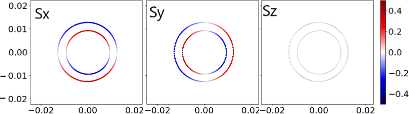
Moreover, due to the lack of the horizontal mirror symmetry, Janus monolayer should have Rashba effect. To examine the Rashba effect, the in-plane spin-textures are calculated, and the Figure 6 shows the spin projected constant energy (0.25 eV above the Fermi level) contour plots of the spin textures calculated in - plane centered at the point. It is clearly seen that the pair of spin-splitting bands for both and spin components have opposite spin orientation. The pure 2D Rashba spin splitting at the conduction bands around point near the Fermi level is observed due to existing concentric spin-texture circles. It is found that only in-plane and spin components are present in the Rashba spin split bands with missing out-of-plane component. The in-plane spin moments of two rings have opposite chirality. The large ring is clockwise, while the small ring is anticlockwise.
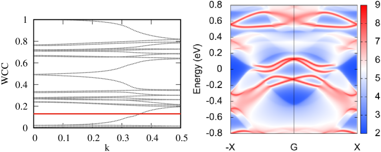
The monolayer / is predicted to be a QSHIq10 . It is natural to confirm the topological properties of Janus monolayer , which can be characterized by the topological invariant. For a material with space inversion symmetry, the can be calculated by calculating the parities of the occupied valence bands by using Fu and Kane s methodf1 , like monolayer /q10 . The universal method is to calculate the Wannier Charge Centers (WCCs), which is used for monolayer . The evolution of WCCs for monolayer is plotted in Figure 7. Taking an arbitrary horizontal line (e.g. WCC=0.13) as reference, one can see that the number of crossings between the reference line and the evolution of WCCs is odd, which verifies that =1. This means that Janus monolayer is a QSHI. Furthermore, a QSHI should exhibit topological protected conducting helical edge states. The Green’s-function method is used to calculate the edge states on (100) edge based on the tight-binding Hamiltonian, which are shown in Figure 7. It is clearly seen that there is a pair of gapless non-trivial edge states, which connect the conduction and valence bands. The edges states exhibit two quadratic dispersive branches with opposite spin. The Dirac point is pushed above the Fermi level, and the Rashba-like splitting states can be observed. Similar phenomenon can be found in monolayer q10 .
In practical application, a substrate is likely to introduce strain to a 2D material due to lattice mismatch. A biaxial in-plane strain is used to study the robustness of the related physical properties of Janus monolayer against the strain effects. We use (0.94-1.06) to simulate biaxial in-plane strain, where and represent the in-plane lattice constants with and without strain, respectively. The strained energy band structures with both GGA and GGA+SOC are plotted in FIG.1 and FIG.2 of electronic supplementary information (ESI). Except for 0.94 strain, they all show direct band-gap semiconductors with both CBM and VBM at K point. For 0.94 strain, GGA results show a metal, but GGA+SOC results demonstrate an indirect band-gap semiconductor with CBM and VBM at and K points. The energy band gaps with both GGA and GGA+SOC and spin-splittings at the K point for LCB and UVB as a function of strain are plotted in FIG.3 and FIG.4 of ESI. These gaps (except for 0.94 strain) and spin-splittings are greater than the thermal energy of room temperature (25 meV), which is necessary to readily access and manipulate valleys for memory and logic applications. Finally, we calculate at all strain points to confirm topological properties of strained monolayer , and only show the evolution of WCCs at 0.94 and 1.06 strains in FIG.5 of ESI. The calculated results show that the WCCs can be crossed only one time by an arbitrary horizontal line, which means =1. These confirm that all strained monolayer are TIs. These imply that the spin-valley coupling and nontrivial topological state are robust against the biaxial strain.
V Discussions and Conclusion
In summary, our calculated results demonstrate that svc-QSHI with spin and valley polarized states can emerge in the Janus monolayer . Particularly, the monolayer hosts Rashba-splitting edges sates, which can be measured by angle-resolved photoemission spectroscopy (ARPES). Furthermore, we demonstrate that the spin-valley-coupling and topological properties are perfectly preserved, when a suitable biaxial strain is applied. In view of the recent experimental progress in type atomic sheetsq6 and Janus monolayerse1 ; e2 , our findings can promote further experimental exploration for intriguing svc-QSHI.
Acknowledgements.
This work is supported by Natural Science Basis Research Plan in Shaanxi Province of China (2021JM-456). We are grateful to the Advanced Analysis and Computation Center of China University of Mining and Technology (CUMT) for the award of CPU hours and WIEN2k/VASP software to accomplish this work.References
- (1) D. Xiao, G. B. Liu, W. Feng, X. Xu and W. Yao, Phys. Rev. Lett. 108, 196802 (2012).
- (2) K. F. Mak, K. L. McGill, J. Park and P. L. McEuen, Science 344, 1489 (2014).
- (3) J. R. Schaibley, H. Yu, G. Clark, P. Rivera, J. S. Ross, K. L. Seyler, W. Yao and X. Xu, Nat. Rev. Mater. 1, 16055 (2016).
- (4) D. Xiao, W. Yao and Q. Niu, Phys. Rev. Lett. 99, 236809 (2007).
- (5) M. Ezawa, Phys. Rev. B 87, 155415 (2013).
- (6) Z. F. Liu, W. X. Feng, H. L. Xin, Y. L. Gao, P. F. Liu, Y. G. Yao, H. M. Weng and J. J. Zhao, Mater. Horiz. 6, 781 (2019).
- (7) M. Z. Hasan and C. L. Kane, Rev. Mod. Phys. 82, 3045 (2010).
- (8) X. L. Qi and S. C. Zhang, Rev. Mod. Phys. 83, 1057 (2011).
- (9) C. L. Kane and E. J. Mele, Phys. Rev. Lett. 95, 226801 (2005).
- (10) M. Konig, S. Wiedmann, C. Brune et al., Science 318, 766 (2007).
- (11) I. Knez, R. R. Du and G. Sullivan, Phys. Rev. Lett. 107, 136603 (2011).
- (12) C. C. Liu, W. Feng and Y. Yao, Phys. Rev. Lett. 107, 076802 (2011).
- (13) S. Zhou, C. C. Liu, J. J. Zhao and Y. G. Yao, npj Quant. Mater. 3, 16 (2018).
- (14) S. Murakami, Phys. Rev. Lett. 97, 236805 (2006).
- (15) J. J. Zhou, W. X. Feng, C. C. Liu, S. Guan and Y. G. Yao, Nano Lett. 14, 4767 (2014).
- (16) Y. Xu, B. Yan, H. J. Zhang et al., Phys. Rev. Lett. 111, 136804 (2013).
- (17) H. M. Weng, X. Dai and Z. Fang, Phys. Rev. X 4, 011002 (2014).
- (18) H. Yanagisawa, Y. Ishida, T. Tanaka, A. Ueno, S. Otani and C. Oshima, Surf. Sci. 600, 4072 (2006).
- (19) Z. Zhao, T. Yu, S. Zhang, H. Xu, G. Yang and Y. Liu, J. Mater. Chem. A 7, 405 (2019).
- (20) C. Kamal, Phys. Rev. B 100, 205404 (2019).
- (21) M. S. Ramzan, V. Bacic, Y. Jing and A. Kuc, J. Phys. Chem. C 123, 25470 (2019).
- (22) S. S. Wang, W. C. Sun and S. Dong, Phys. Chem. Chem. Phys. 23, 2134 (2021).
- (23) H. W. Xu, H. Wang, J. Zhou, Y. F. Guo, J. Kong and J. Li, npj Computational Materials 7, 31 (2021).
- (24) P. Hohenberg and W. Kohn, Phys. Rev. 136, B864 (1964); W. Kohn and L. J. Sham, Phys. Rev. 140, A1133 (1965).
- (25) G. Kresse, J. Non-Cryst. Solids 193, 222 (1995).
- (26) G. Kresse and J. Furthmller, Comput. Mater. Sci. 6, 15 (1996).
- (27) G. Kresse and D. Joubert, Phys. Rev. B 59, 1758 (1999).
- (28) J. P. Perdew, K. Burke and M. Ernzerhof, Phys. Rev. Lett. 77, 3865 (1996).
- (29) A. Togo, F. Oba, and I. Tanaka, Phys. Rev. B 78, 134106 (2008).
- (30) Q. Wu, S. Zhang, H. F. Song, M. Troyer and A. A. Soluyanov, Comput. Phys. Commun. 224, 405 (2018).
- (31) A. A. Mostofia, J. R. Yatesb, G. Pizzif, Y.-S. Lee, I. Souzad, D. Vanderbilte and N. Marzarif, Comput. Phys. Commun. 185, 2309 (2014).
- (32) U. Herath, P. Tavadze, X. He, E. Bousquet, S. Singh, F. Munoz and A. H. Romero, Computer Physics Communications 251, 107080 (2020).
- (33) A.-Y. Lu, H. Zhu, J. Xiao, C.-P. Chuu, Y. Han, M.-H. Chiu, C.-C. Cheng, C.-W. Yang, K.-H. Wei, Y. Yang, Y. Wang, D. Sokaras, D. Nordlund, P. Yang, D. A. Muller, M.-Y. Chou, X. Zhang and L.-J. Li, Nat. Nanotechnol. 12, 744 (2017).
- (34) J. Zhang, S. Jia, I. Kholmanov, L. Dong, D. Er, W. Chen, H. Guo, Z. Jin, V. B. Shenoy, L. Shi and J. Lou, ACS Nano 11, 8192 (2017).
- (35) E. Mariani and F. V. Oppen, Phys. Rev. Lett. 100, 076801 (2008).
- (36) J. Carrete , W. Li, L. Lindsay, D. A. Broido, L. J. Gallego and N. Mingo, Mater. Res. Lett. 4, 204 (2016).
- (37) R. C. Andrew, R. E. Mapasha, A. M. Ukpong and N. Chetty, Phys. Rev. B 85, 125428 (2012).
- (38) E. Cadelano, P. L. Palla, S. Giordano and L. Colombo, Phys. Rev. B 82, 235414 (2010).
- (39) L. Dong, J. Lou and V. B. Shenoy, ACS Nano, 11, 8242 (2017).
- (40) M. N. Blonsky, H. L. Zhuang, A. K. Singh and R. G. Hennig, ACS Nano, 9, 9885 (2015).
- (41) S. D. Guo, Y. T. Zhu, W. Q. Mu and W. C. Ren, EPL 132, 57002 (2020).
- (42) L. Fu and C. L. Kane, Phys. Rev. B 76, 045302 (2007).