[figure]labelfont=bf,name=Fig.,labelsep=colon \alsoaffiliationDiamond Light Source, Chilton OX11 0DE, United Kingdom \alsoaffiliationInstitute of Physics, Czech Academy of Sciences, 162 00 Praha 6, Czech Republic
Defect-driven antiferromagnetic domain walls in CuMnAs films
Abstract
Efficient manipulation of antiferromagnetic (AF) domains and domain walls has opened up new avenues of research towards ultrafast, high-density spintronic devices. AF domain structures are known to be sensitive to magnetoelastic effects, but the microscopic interplay of crystalline defects, strain and magnetic ordering remains largely unknown. Here, we reveal, using photoemission electron microscopy combined with scanning X-ray diffraction imaging and micromagnetic simulations, that the AF domain structure in CuMnAs thin films is dominated by nanoscale structural twin defects. We demonstrate that microtwin defects, which develop across the entire thickness of the film and terminate on the surface as characteristic lines, determine the location and orientation of and domain walls. The results emphasize the crucial role of nanoscale crystalline defects in determining the AF domains and domain walls, and provide a route to optimizing device performance.
1 Introduction
A key goal of spintronics is the development of high-speed, high-density data storage devices that are robust against magnetic fields. Antiferromagnetic (AF) materials offer a route to realising these goals since they exhibit intrinsic dynamics in the THz-regime, lack magnetic stray fields and can be electrically switched1, 2, 3, 4. Moreover, AF order is exhibited in a wide range of materials compatible with the properties of insulators, semiconductors and metals. Electrical switching has been achieved in several AF systems, with the resulting current-induced domain modifications attributed to spin-orbit torques or thermomagnetoelastic effects 4, 5, 6, 7. Spin-orbit torque manipulation of AF domains was first achieved using orthogonal current pulses to induce rotations of the AF order parameter, but more recently current-polarity dependent switching of AF order has been achieved and ascribed to domain wall motion 8. AF domains and domain walls are therefore the building blocks of AF spintronics, but pinning can limit device performance whilst creep affects long-term memory stability. In ferro- and ferrimagnets, magnetic domain formation has been extensively studied for decades and is well-known to be largely governed by the minimization of the demagnetizing field energy 9, 10. On the other hand, domain formation in fully compensated antiferromagnets remains largely unexplored.
Domain morphologies in AF thin films vary considerably with thickness and nanostructure shape which has been ascribed to strain effects, although evidence for a direct relationship is lacking 11, 12, 13, 14, 15. To date, device concepts have considered an ideal AF spin lattice 3, 16, 17, but high-resolution AF domain imaging has revealed pronounced non-uniformities and pinning effects during domain switching 18, 8, 19, 5, 20, 6.
The metallic antiferromagnet CuMnAs is a focus of AF spintronics research due to its favorable crystal symmetry for spin-orbit torque switching. In CuMnAs thin films, elongated microtwins and atomically sharp anti-phase boundaries 21 have recently been identified as the most prominent defects. The anti-phase boundaries have been associated with atomically sharp AF domain walls 22. The microtwin defects, which are the focus of this work, are shown to have a dramatic influence on the AF domain configuration in CuMnAs thin films. We show that microtwin defects largely control the domain structure by generating pinned domain walls and confining domain walls.
2 Results
The thick CuMnAs(001) films were grown epitaxially on GaP(001) 21. The CuMnAs layer is a collinear antiferromagnet with a Néel temperature of 23 and a tetragonal crystal structure (, ). Close lattice-matching along the half-diagonal of the cubic GaP substrate unit cell ensures fully strained epitaxial growth with low mosaicity 24. The spin axes align in the -plane, i.e. in the plane of the film 25 due to a strong magnetocrystalline anisotropy. In the following the crystallographic axes refer to the orientation of the CuMnAs crystal.
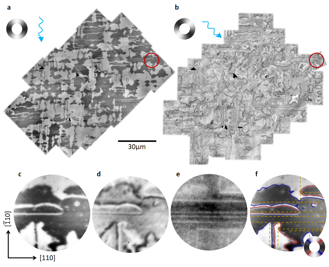
The AF domain structure was imaged using high-resolution photoemission electron microscopy (PEEM) combined with X-ray magnetic linear dichroism (XMLD) 26. Figures 1 a and 1 b show large area maps imaged with the X-ray polarization vector () aligned to highlight the AF domain structure and domain boundaries, respectively. Maximum XMLD contrast is observed between regions with the local spin axis aligned perpendicular and parallel to . We observe approximately equal populations of light and dark areas in Fig. 1 a, corresponding to domains with the local spin axis parallel to or (see Supplementary Note 1). Figures 1 c and d show high-resolution XMLD-PEEM images of the red circled area in Fig. 1 a and b. The AF domains typically exceed several in lateral size and generally have serrated edges.
The boundaries between the domains are visible in Fig. 1 b and d, when is at to the local spin axis in both AF domains. In this imaging configuration, the domains have the same contrast and the domain boundary contrast dominates. domain walls appear as well separated black or white lines, depending on the average direction of the spin axis across the domain wall, with typical width (40050) nm. Adjacent black and white lines in Fig. 1 b and d correspond to domain walls (see Supplementary Note 2).
X-ray Linear Dichroism (XLD) combined with PEEM is sensitive to local changes in the charge anisotropy and can therefore act as an indicator of local crystallographic variations, structural defects. Figure 1 e shows an XLD-PEEM image of the red circled area in Fig. 1 a and b which reveals a pattern of thin lines running parallel to the and crystallographic directions. Figure 1 f shows the AF domain structure superimposed with the domain wall contrast (blue and red lines) along with the structural defect pattern (broken yellow lines). Direct comparison of the XMLD-PEEM and XLD-PEEM images over the same area shows that the local AF spin axis is always oriented collinear with the defect lines.
Long straight domain walls are found to be confined between two parallel defects. These domain walls extend over several microns and can be seen as the long, thin light and dark lines in Fig. 1 a. In some cases these domain walls become highly constricted between two neighboring defects as seen in the middle of Fig. 1 f. The domain walls form corners in areas where two defects are orthogonal, as for example in the bottom half of Fig. 1 f, which form the serrated edges seen in Fig. 1 a.
Bulk-sensitive crystallographic information on the nature of defects in thin films, with nanoscale spatial resolution, can be achieved using scanning X-ray diffraction microscopy (SXDM) 27. Crystallographic defects lead to specific contributions to a reciprocal space map (RSM). A three-dimensional RSM of the CuMnAs (003) Bragg peak, generated from two-dimensional diffraction images for several sample tilts (see Methods and Supplementary Note 3) is shown in Fig. 2 a. The RSM has a modulated intensity along arising from the finite film thickness 28 as well as strong diffuse scattering along the -type directions, which has been attributed to anti-phase boundaries along the planes 21. Sharper intensity streaks, hereafter referred to as wings, along the -type directions indicate the presence of another type of defect. These wings are only visible for specific areas of the sample and are marked by the colored ovals in the lower panel of Fig. 2 a.
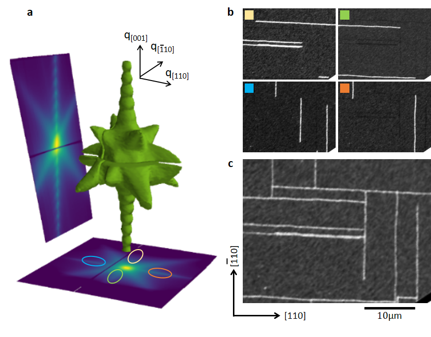
Mapping the intensity of these wings generates real-space images of the defects. Maps produced using the intensity of one of the wings yield bright defect lines, on a homogeneous background, which run perpendicular to the direction of the selected wing, see Fig. 2 b. The lines obtained from separate wings are complementary to each other, i.e. each wing produces a separate set of lines. The collated lines arising from all wings are given in Fig. 2 c which reveals a rectangular pattern of defect lines running along the and directions, reminiscent of the pattern revealed by XLD-PEEM in Fig. 1 e. The four complementary sets of defect lines with specific -dependence of the scattering revealed by SXDM indicate defect orientations along four different crystallographic directions in the bulk, while the XLD-PEEM images only show their surface termination.
High-angle annular dark field-scanning transmission electron microscopy (HAADF-STEM) reveals that the defects are slabs of a microtwinned phase, in which the lattice is rotated so that the -axis is tilted away from the film normal by , as shown in Fig. 3 a and b. The slabs extend over most of the film thickness and grow wider towards the sample surface where they produce the characteristic rectangular pattern with lines running parallel to the and directions, Fig. 3 c. Figure 3 b shows a high-resolution image of a microtwin defect where the atomic ordering is indicated. The microtwin and surrounding bulk film form a coherent boundary, with the microtwin slab extending along one of the planes. In particular, for each defect line on the surface there are two possible bulk defect slab orientations with opposite tilts 21 which can be distinguished in SXDM, but not in XLD-PEEM.
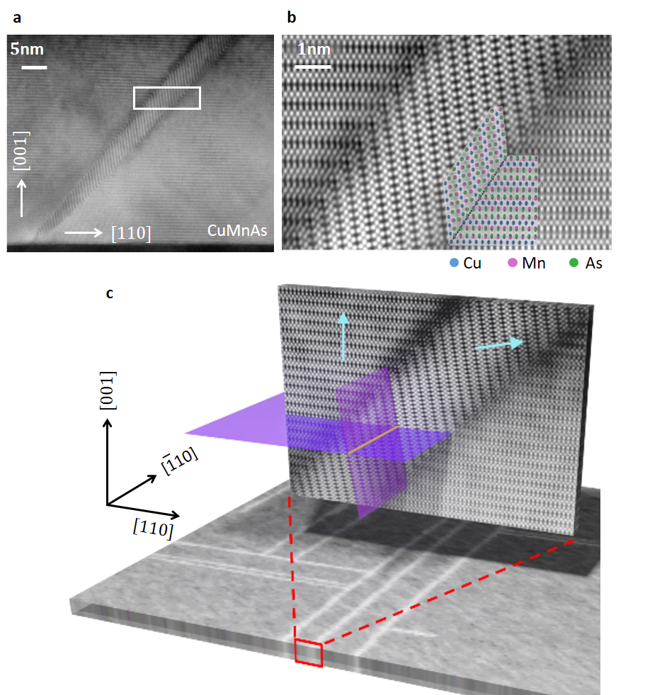
As the magnetic easy-plane in tetragonal CuMnAs is perpendicular to the -axis 25, the rotation of the -axis in the microtwin region will have a profound effect on the local spin orientation. The microtwin region and surrounding bulk film share only one magnetic easy axis, determined by the intersection of the easy planes (purple sheets in Fig. 3 c). This easy axis is represented by the orange line in Fig. 3 c. For any microtwin defect line on the surface, there are two possible propagation directions into the bulk, but for either case the easy axis remains parallel to the defect line on the surface. The local Néel vectors (i.e. the difference in the sublattice magnetic moment directions) then aligns parallel to the microtwin surface termination. For adjacent microtwin defects, the local Néel vector can align either parallel or antiparallel. Antiparallel alignment results in the domain walls seen in the XMLD-PEEM images in Fig. 1. For parallel alignment of the Néel vector, the area between the microtwin defects is magnetically homogeneous and can extend over several microns. Perpendicular alignment of two defects gives rise to domain walls.
In the final part, we show that including the effects of microtwin defects in micromagnetic simulations is sufficient to fully explain the experimentally observed AF domain structures shown in Fig. 1. The simulations consider an AF layer with two (equivalent) orthogonal in-plane easy axes, i.e. without considering an out-of-plane variation of the Néel vector. The effects of microtwins are included as a rotation of the magnetocrystalline anisotropy localized at the microtwins along with a homogeneous strain field, perpendicular to the microtwins (see Supplementary Note 4). We consider that the extrinsic strain due to the microtwin is much larger than the spontaneous strains due to the magnetic texture, such that the inverse effect of the magnetic texture on the strain distribution 29 can be neglected. The simulations show that the spin axis in the vicinity of a microtwin defect line is always aligned parallel to the defect line.
Figures 4 a and b show the simulated AF domain structures for two parallel microtwin defect lines with a different spacing between the lines. For this configuration, antiparallel alignment of the Néel vectors on either side of the microtwin defects results in a domain wall. For large separations of the microtwins, the domain wall width is determined by the strain-induced magnetic anisotropy. For small separations, the rotated magnetocrystalline anisotropy of the microtwin defects leads to a narrower, highly confined domain wall. The simulations show a close resemblance to the XMLD-PEEM image of the AF domain wall shown in the middle of Fig. 4 e. The domain wall is narrow and straight in the confined area on the left of Fig. 4 e whereas it becomes wider and meanders on the right of the image where the microtwin defects are much further apart.
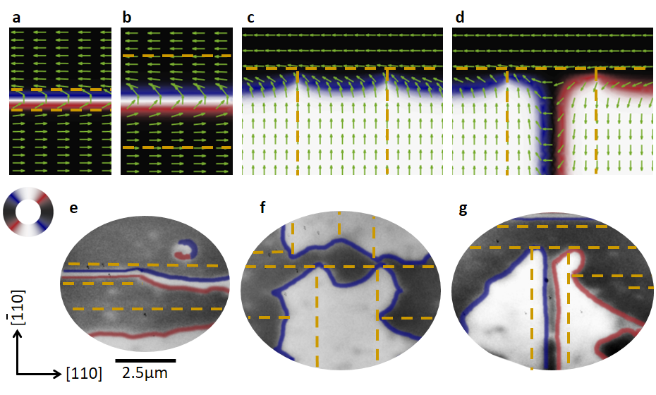
Figures 4 c and d show simulated AF domain structures for two parallel microtwin defect lines terminating on a perpendicular mircotwin defect line for two different initial boundary configurations. For a parallel boundary configuration of the Néel vectors across the two parallel defect lines (Fig. 4 c), the simulations converge to a homogeneous AF domain configuration across the defect lines (see lower half of Fig. 4 c). On the other hand, a domain wall forms close to the perpendicular defect line with characteristic pinch points close to the T-junctions reminiscent of the serrated edges seen on the AF domains in the experiment (Fig. 4 f). A similar result is found for an antiparallel initial boundary configuration, but with an additional domain wall between the parallel defect lines. This domain wall unzips into two domain walls with opposite senses of rotation along with pinch points at the T-junctions. The simulation closely reproduces the AF configuration imaged using XMLD-PEEM (Fig. 4 g).
3 Discussion
The microscopic AF domain structure in CuMnAs thin films has been shown to be dominated by microtwin defects that appear as lines along specific crystallographic directions on the film surface. The local spin axis is aligned parallel to the defect lines. This then leads to either large AF domains with serrated edges or domain walls running parallel to the or crystallographic directions. A perpendicular orientation of two microtwin defect lines leads to domains walls that lead to domain boundaries with serrated edges. The micromagnetic simulations, with the inclusion of local strain-fields arising from the microtwin defects, reproduce all the principal building blocks of the entire AF domain structure observed in CuMnAs thin films. Furthermore, the simulations highlight the variety of domain and domain wall structures possible when an array of microtwin defects govern the AF ordering.
Our results emphasize the sensitivity of AF domain structures to defect structures in thin films. The concentration of such defects may be engineered by varying the growth parameters, particularly the substrate temperature and Cu/Mn stoichiometry 21, providing a mechanism for tailoring the AF domains and domain walls for specific functionality. Introducing some bias during growth, such as substrate stress or miscut angle, may allow further control over the distribution of defect orientations. In terms of optimization of device performance, it was shown previously that the largest electrical readout signals after current pulsing are observed for growth conditions corresponding to the lowest defect densities 21. This is an indirect indication that the microtwin defects inhibit the nucleation and switching of antiferromagnetic domains. On the other hand, the control of microtwin defects may be beneficial for current-driven motion of antiferromagnetic domain walls between well-defined pinning centres 8. Thus, developing high-performance spintronic devices will rely on a detailed understanding of the nanoscale coupling between the local AF order and the crystallographic microstructure.
4 Methods
4.1 Sample fabrication
The CuMnAs films were grown by molecular beam epitaxy on a GaP buffer layer on a GaP(001) substrate and capped with a Al film to prevent surface oxidation for the PEEM imaging.
4.2 PEEM Imaging
The PEEM measurements were performed on beamline I06 at Diamond Light Source, using linearly polarized X-rays incident at to the film surface. Magnetic contrast with spatial resolution was obtained from the asymmetry between images recorded using photon energies corresponding to the maximum and minimum of the Mn XMLD spectrum (see Supplementary Note 1). The linear polarization () was in the plane of the film, and the largest magnetic contrast was obtained between AF domains with spin axes parallel and perpendicular to . The XMLD spectrum has a a similar lineshape, but opposite sign, for and (Ref. 23). PEEM images with sensitivity to the microtwin configuration were obtained from the asymmetry between images recorded at photon energies corresponding to the maximum and minimum of the Mn non-magnetic XLD spectrum (see Supplementary Note 1) with at to the surface. All measurements were performed at room temperature.
4.3 Scanning X-ray diffraction microscopy
SXDM was performed on the NanoMAX-beamline at MAX IV Laboratory 30. The beam was focused to a lateral diameter of and the X-ray energy tuned to . The measurement geometry was determined by three angles: the detector angle () measured from the direction of the incident beam in the vertical plane, which defines the angle of incidence with respect to the sample surface in the vertical diffraction plane and which defines the sample azimuth. The sample was scanned laterally over a 2D-mesh at a fixed sample orientation with a diffraction image recorded at each position. The imaging was performed using a Merlin Si Quad area detector with pixels, each in size. The distance between the detector and sample was .
RSMs were constructed via several 2D-mesh scans with a stepsize of at different angles around the (003) Bragg reflection in increments. For these measurements was chosen such that the X-ray beam impinged along the CuMnAs direction. Analysis was performed using the xrayutilities toolbox described in reference 31.
SXDM imaging of the microtwin configuration was performed with chosen so that the beam impinged along the CuMnAs direction. The microtwin configuration was mapped with the sample at an angle from the Bragg angle. For each angle, the detector plane sliced through two of the microtwin-related wings in reciprocal space. Consequently, if a microtwin was in the illuminated area, significantly higher intensity was recorded on the corresponding area of the detector, depending on the microtwin orientation. Mapping these areas of high intensity thus revealed the spatial pattern of microtwins with a specific orientation. The SXDM map shown in Fig. 2 c is the sum of SXDM images recorded with and . For details see Supplementary Note 3.
4.4 Transmission Electron Microscopy
For the HAADF-STEM measurements, the CuMnAs samples were capped with an additional - of carbon ex situ and tungsten in situ. Thin lamellae were prepared by a Ga focused ion beam. The lamellae were polished at and . The lamellae were investigated using a FEI Titan Themis 60-300 cubed high-resolution (scanning) transmission electron microscope at . The atomic model overlay shown in Fig. 3 b was produced using VESTA software 32.
4.5 Micromagnetic Simulations
The distribution of the Néel vector in the presence of different microtwin configurations was simulated using the Matlab PDE Toolbox to solve the micromagnetic equation
| (1) |
with von Neumann boundary conditions. Here is the magnetic stiffness, is the Laplace operator, and
| (2) |
where , and are the densities of magnetic anisotropy energy of the bulk film, the magnetic anisotropy energy of the microtwin, and the magnetoelastic energy, respectively. Details can be found in Supplementary Note 4.
References
- Jungwirth et al. 2016 Jungwirth, T.; Marti, X.; Wadley, P.; Wunderlich, J. Antiferromagnetic spintronics. Nat. Nanotechnol. 2016, 11, 231–241
- Baltz et al. 2018 Baltz, V.; Manchon, A.; Tsoi, M.; Moriyama, T.; Ono, T.; Tserkovnyak, Y. Antiferromagnetic spintronics. Rev. Mod. Phys. 2018, 90, 015005
- Z̆elezný et al. 2014 Z̆elezný, J.; Gao, H.; Výborný, K.; Zemen, J.; Mas̆ek, J.; Manchon, A.; Wunderlich, J.; Sinova, J.; Jungwirth, T. Relativistic Néel-Order Fields Induced by Electrical Current in Antiferromagnets. Phys. Rev. Lett. 2014, 113, 157201
- Wadley et al. 2016 Wadley, P. et al. Electrical switching of an antiferromagnet. Science 2016, 351, 587–590
- Baldrati et al. 2019 Baldrati, L.; Gomonay, O.; Ross, A.; Filianina, M.; Lebrun, R.; Ramos, R.; Leveille, C.; Fuhrmann, F.; Forrest, T. R.; Maccherozzi, F.; Valencia, S.; Kronast, F.; Saitoh, E.; Sinova, J.; Kläui, M. Mechanism of Néel Order Switching in Antiferromagnetic Thin Films Revealed by Magnetotransport and Direct Imaging. Phys. Rev. Lett 2019, 123, 177201
- Kašpar et al. 2021 Kašpar, Z. et al. Quenching of an antiferromagnet into high resistivity states using electrical or ultrashort optical pulses. Nature Electron. 2021, 4, 30
- Meer et al. 2021 Meer, H.; Schreiber, F.; Schmitt, C.; Ramos, R.; Saitoh, E.; Gomonay, O.; Sinova, J.; Baldrati, L.; Kläui, M. Direct Imaging of Current-Induced Antiferromagnetic Switching Revealing a Pure Thermomagnetoelastic Switching Mechanism in NiO. Nano Lett. 2021, 21, 114
- Wadley et al. 2018 Wadley, P.; Reimers, S.; Grzybowski, M. J.; Andrews, C.; Wang, M.; Chauhan, J. S.; Gallagher, B. L.; Campion, R. P.; Edmonds, K. W.; Dhesi, S. S.; Maccherozzi, F.; Novak, V.; Wunderlich, J.; Jungwirth, T. Current polarity-dependent manipulation of antiferromagnetic domains. Nat. Nanotechnol. 2018, 13, 362–365
- Hubert and Schäfer 1998 Hubert, A.; Schäfer, R. Magnetic Domains: The Analysis of Magnetic Microstructures; Springer, 1998
- McCord 2015 McCord, J. Progress in magnetic domain observation by advanced magneto-optical microscopy. Journal of Physics D: Applied Physics 2015, 48, 333001
- Menon et al. 2011 Menon, K. S. R.; Mandal, S.; Das, J.; Menteş, T. O.; Niño, M. A.; Locatelli, A.; Belkhou, R. Surface antiferromagnetic domain imaging using low-energy unpolarized electrons. Phys. Rev. B 2011, 84, 132402
- Scholl et al. 2000 Scholl, A.; Stohr, J.; Lüning, J.; Seo, J. W.; Fompeyrine, J.; Siegwart, H.; Locquet, J.-P.; Nolting, F.; Anders, S.; Fullerton, E. E.; Scheinfein, M. R.; Padmore, H. A. Observation of Antiferromagnetic Domains in Epitaxial Thin Films. Science 2000, 287, 1014–1016
- Folven et al. 2010 Folven, E.; Tybell, T.; Scholl, A.; Young, A. T.; Retterer, S. T.; Takamura, Y.; Grepstad, J. K. Antiferromagnetic Domain Reconfiguration in Embedded LaFeO3 Thin Film Nanostructures. Nano Lett. 2010, 10, 4578–4583
- Bezencenet et al. 2011 Bezencenet, O.; Bonamy, D.; Belkhou, R.; Ohresser, P.; Barbier, A. Origin and Tailoring of the Antiferromagnetic Domain Structure in -Fe2O3 Thin Films Unraveled by Statistical Analysis of Dichroic Spectromicroscopy Images. Phys. Rev. Lett. 2011, 106, 107201
- Folven et al. 2015 Folven, E.; Linder, J.; Gomonay, O. V.; Scholl, A.; Doran, A.; Young, A. T.; Retterer, S. T.; Malik, V. K.; Tybell, T.; Takamura, Y.; Grepstad, J. K. Controlling the switching field in nanomagnets by means of domain-engineered antiferromagnets. Phys. Rev. B 2015, 92, 094421
- Khymyn et al. 2017 Khymyn, R.; Lisenkov, I.; Tiberkevich, V.; Ivanov, B. A.; Slavin, A. Antiferromagnetic THz-frequency Josephson-like Oscillator Driven by Spin Current. Sci. Rep. 2017, 7, 43705
- Gomonay et al. 2018 Gomonay, O.; Jungwirth, T.; Sinova, J. Narrow-band tunable terahertz detector in antiferromagnets via staggered-field and antidamping torques. Phys. Rev. B 2018, 98, 104430
- Grzybowski et al. 2017 Grzybowski, M. J.; Wadley, P.; Edmonds, K. W.; Beardsley, R.; Hills, V.; Campion, R. P.; Gallagher, B. L.; Chauhan, J. S.; Novak, V.; Jungwirth, T.; Maccherozzi, F.; S., D. S. Imaging Current-Induced Switching of Antiferromagnetic Domains in CuMnAs. Phys. Rev. Lett. 2017, 118, 057701
- Bodnar et al. 2019 Bodnar, S. Y.; Filianina, M.; Bommanaboyena, S. P.; Forrest, T.; Maccherozzi, F.; Sapozhnik, A. A.; Skourski, Y.; Kläui, M.; Jourdan, M. Imaging of current induced Néel vector switching in antiferromagnetic Mn2Au. Phys. Rev. B 2019, 99, 140409
- Janda et al. 2020 Janda, T. et al. Magneto-Seebeck microscopy of domain switching in collinear antiferromagnet CuMnAs. Phys. Rev. Mater. 2020, 4, 094413
- Krizek et al. 2020 Krizek, F. et al. Molecular beam epitaxy of CuMnAs. Phys. Rev. Materials 2020, 4, 014409
- Krizek et al. 2021 Krizek, F. et al. Atomically sharp domain walls in an antiferromagnet. 2021
- Wadley et al. 2015 Wadley, P. et al. Antiferromagnetic structure in tetragonal CuMnAs thin films. Scientific Reports 2015, 5, 17079
- Wadley et al. 2013 Wadley, P. et al. Tetragonal phase of epitaxial room-temperature antiferromagnet CuMnAs. Nat. Commun. 2013, 4, 2322
- Wadley et al. 2015 Wadley, P. et al. Control of antiferromagnetic spin axis orientation in bilayer Fe/CuMnAs films. Sci. Rep. 2015, 5, 17079
- Wadley et al. 2017 Wadley, P.; Edmonds, K. W.; Shahedkhah, M. R.; Campion, R. P.; Gallagher, B. L.; Zelezny, J.; Kunes, J.; Novak, V.; Jungwirth, T.; Saidl, V.; Nemec, P.; Maccherozzi, F.; Dhesi, S. S. Control of antiferromagnetic spin axis orientation in bilayer Fe/CuMnAs films. Sci. Rep. 2017, 7, 11147
- Stangl et al. 2013 Stangl, J.; Mocuta, C.; Chamard, V.; Carbone, D. Nanobeam X‐Ray Scattering; John Wiley & Sons, Ltd, 2013
- Pietsch et al. 2004 Pietsch, U.; Holy, V.; Baumbach, T. High-Resolution X-Ray Scattering: From Thin Films to Lateral Nanostructures; Advanced Texts in Physics; Springer New York, 2004
- Gomonay and Loktev 2002 Gomonay, H.; Loktev, V. M. Magnetostriction and magnetoelastic domains in antiferromagnets. J. Phys. C 2002, 14, 3959–3971
- 30 Carbone, D.; et al., Design and Performance of NanoMAX diffraction endstation, manuscript in preparation for Journal of Synchrotron Radiation
- Kriegner et al. 2013 Kriegner, D.; Wintersberger, E.; Stangl, J. xrayutilities: a versatile tool for reciprocal space conversion of scattering data recorded with linear and area detectors. Journal of Applied Crystallography 2013, 46, 1162–1170
- Momma and Izumi 2011 Momma, K.; Izumi, F. VESTA3 for three-dimensional visualization of crystal, volumetric and morphology data. Journal of Applied Crystallography 2011, 44, 1272–1276
5 Acknowledgements
We thank Diamond Light Source for the allocation of beamtime on beamline I06 under Proposal nos. MM22437-1 and NT27146-1. We acknowledge MAX IV Laboratory for beamtime on Beamline NanoMAX under Proposal C20190533. Research conducted at MAX IV, a Swedish national user facility, is supported by the Swedish Research Council under contract 2018-07152, the Swedish Governmental Agency for Innovation Systems under contract 2018-04969, and Formas under contract 2019-02496. CzechNanoLab project LM2018110 funded by MEYS CR is gratefully acknowledged for the financial support of the measurements and sample fabrication at CEITEC Nano Research Infrastructure. The work was supported by the EU FET Open RIA Grant no 766566 and the Ministry of Education of the Czech Republic Grant No. LM2018110, and LNSM-LNSpin, and the Grant Agency of the Czech Republic Grant No. 19-28375X.
6 Author contributions
SSD, KWE and PW conceived and led the project. SSD, KWE and SR devised the XMLD-PEEM and XLD-PEEM imaging and performed the measurements with FM, OJA, LXB, SFP, KAO and PW. The SXDM experiment were performed by SR, DK, AB, KWE, SSD. DK and DC coordinated and supervised the SXDM data analysis and the interpretation of the results with help from SR. OG developed the micromagnetic simulations with feedback from SSD, KWE and SR. FK, JM and OM performed the HAADF-STEM experiments and data analysis. SR combined and led the analysis of the data from the different experimental techniques. RPC, FK and VN fabricated the samples. SSD, KWE and SR wrote the manuscript with feedback from all authors.
7 Competing Interests
The authors declare no competing interests.