Autonomous Investigations over WS2 and Au{111} with Scanning Probe Microscopy
1 Abstract
Individual atomic defects in 2D materials impact their macroscopic functionality. Correlating the interplay is challenging, however, intelligent hyperspectral scanning tunneling spectroscopy (STS) mapping provides a feasible solution to this technically difficult and time consuming problem. Here, dense spectroscopic volume is collected autonomously via Gaussian process regression, where convolutional neural networks are used in tandem for spectral identification. Acquired data enable defect segmentation, and a workflow is provided for machine-driven decision making during experimentation with capability for user customization. We provide a means towards autonomous experimentation for the benefit of both enhanced reproducibility and user-accessibility. Hyperspectral investigations on W sulfur vacancy sites are explored, which is combined with local density of states confirmation on the Au{111} herringbone reconstruction. Chalcogen vacancies, pristine W, Au face-centered cubic, and Au hexagonal close packed regions are examined and detected by machine learning methods to demonstrate the potential of artificial intelligence for hyperspectral STS mapping.
2 Introduction
Two-dimensional (2D) material systems are one of the most sought after solid-state and thin-film structures due to the enormous phase space of functionality, which is driven by atomic- and nano- scale defects that can be advantageously manipulated for single-photon emission, strain engineering, Moiré physics, stacking, and transport.1, 2, 3, 4, 5, 6, 7 Defective perturbations can alter the effective local landscape and immediately impact macroscopic functionality. Scanning tunneling microscopy (STM), one branch of scanning probe microscopy (SPM), remains fundamental for characterizing and understanding material and surface properties at distances within the atomic-to-nano range, providing information at scale into, e.g., spin-orbit coupling effects within chalcogen vacancies, electrically-driven photon emission of individual defects, and substitutional fingerprinting by measuring the local density of states (LDOS). 8, 9, 10, 11 Techniques that provide spectroscopic insight, such as STM, are extremely important in correlating defective states with macroscopic phenomena; hyperspectral data collection in, e.g., tip-enhanced Raman imaging and in optical transmission electron microscopy have become standard and enabled spectroscopic capability with enormous information richness that is both spatially and spectrally resolved.12, 13, 14, 15 However, while hyperspectral STS imaging would provide critical insight into heterogenous electronic properties at the atomic scale, it is not feasible due to the enormous time required. For instance, a hyperspectral optical map collected at 10 min per point in a 150150 pixel grid would take well over one month. Here, we present a means of performing spatially-dense, point spectroscopic measurements with an STM in combination with artificially intelligent and machine learning (AI/ML) approaches to provide a faster and more reproducible approach to map and identify spectroscopic signatures of heterogeneous surfaces.
Since the inception of scanning tunneling spectroscopy (STS), which measures current-voltage (I/V) characteristics, the vast majority of experiments are performed using single pixel spectroscopy, where routes for data collection tend to be geometrically positioned along a line or grid during point acquisition. The first harmonic, within an atomically resolved area, can be measured over a defined voltage range, with lock-in techniques, that corresponds to a convolution of the tip and surface LDOS (dI/dV). Assuming the tip remains constant then the data collected are from the sample alone,16 where inelastic contributions (I/d) can also be inferred from the second harmonic.17 This and other recent spectroscopic capabilities within the STM/STS field have given insight into the electronic structure at the atomic scale relevant for the entire field of surface science, chemical processes, optoelectronic processes, the identification of individual adatoms and molecules on surfaces, local spin-orbit coupling, and electron-phonon coupling, all with sufficient spectroscopic energy resolution to also resolve quantum phase transitions, enable the exploration of next generation color centers, the capability to resolve quantum emitters at scale, or map quantum coherence transport.4, 18, 19, 20, 3 En route towards making STS more widely available, we collect point STS autonomously, via Gaussian process regression, and benchmark our method on tungsten disulfide (WS2) and a Au{111} surface. The methods shown and autonomous experimentation techniques used can be extended to a variety of available spectroscopic techniques within the SPM field, such as force spectroscopy with non-contact atomic force microscopy, however, we first focus on using the LDOS as a tool to identify surface and defective states.
Transition metal dichalcogenides (TMDs), such as WS2, have gained substantial interest for point-defect control,21, 22 serving as host substrates for quantum emitters,23 spin-valley splitting properties,24, 25, 26 and tunable band gap engineering.27, 28, 29 Sulfur vacancies (VS) can be controllably created to serve as target sites for photo- and spin- active functionalization.30, 31 SPM can measure the electronic characteristics at the atomic level of induced defects,21, 24, 26 while also providing a path to excite optical transitions.32 2D TMDs provide a wide phase space to non-destructively modify the quantum environment through a wide variety of defects,24 however a means to probe the electronic environment to produce statistically significant and reproducible spectra is required to expedite the understanding of emerging phenomena within the field. Furthermore, coinage metal surfaces, such as Au, have been widely explored for a variety of applications in, e.g., molecular self-assembly,33, 34 tip-forming,32 and device applications,35, 36 to name a few, and provide a means for tip state calibration with application towards high throughput STS. Hence, W and Au{111} are relevant and representative substrates for both the STM/STS community to employ as model systems and to demonstrate our AI/ML driven approach for hyperspectral STS mapping.
One technical challenge of STM/STS is the difficulty of the technique to acquire reproducible, artifact-free tunneling, especially in heterogeneous samples. Acquisition times are governed by multiple hyperparameters, such as voltage range, step size, and dwell time, where spectral collection that is both highly resolved energetically and spatially is confounded by a variety of factors, which can be very time intensive. In conventional STM/STS, point LDOS exploits the full energetic range of interest with high resolution, and a subsequent dI/dV map can then be collected at a specified energy level for high spatial resolution at the cost of greater experimental broadening. Current imaging tunneling spectroscopy (CITS) consists of scanning the tip in - and - directions within a predefined grid and collecting a high-resolution spectrum at each pixel and can thus visualize spectroscopic nuances spatially, such as band-bending across defective states, that may otherwise be missed.37, 38 CITS takes advantage of both modalities to create a full spectral and spatial picture of a region of interest, but this modality is complicated by any accompanied thermal drift, piezo hysteresis, grid optimization, and time constraints, which can either introduce artifacts in the spectra or limit experimental acquisition. The need for technical approaches that make hyperspectral STS mapping more accessible and user-friendly can provide essential utility into materials discovery and design.
We propose to make use of Gaussian process (GP) regression for hyperspectral data collection,39, 40, 41, 42, 43 which is a well-known method for function approximation and uncertainty quantification. This method refers to a set of function values, where any finite subset of elements have a joint Gaussian distribution. Given some initial input, a Gaussian prior probability density function is learned and then conditioned on data, providing a posterior mean and variance within the model domain, which can be used to make autonomous decisions about optimal point measurements. This and other learning approaches have shown to be useful for hyperspectral image reconstruction,41, 44 autonomous synchrotron experiments,40 materials discovery,43, 45, 46 feature extraction,47 and in piezoresponse force microscopy,48, 41 to name a few applications. The promise of autonomously driven experiments with STM come at the benefit of the human operator and can provide industrial application, where a qualified scientist or engineer can initialize an experiment and allow an AI/ML algorithm to complete the workflow.49, 50, 51, 52, 53, 54, 55
Here, we present one technical approach to address this challenge to perform hyperspectral STS mapping at defect sites on two different surfaces and demonstrate a) how to perform measurements with reproducible spectra, and b) create statistically significant electronic characterization of the different intrinsic defects that can be found on samples of interest. While this does not enhance sample throughput directly, it allows for samples to be spectroscopically and automatically interrogated in terms of defect diversity and their electronic fingerprint, such that a non-STM expert would have the ability to produce relevant spectroscopic insight after little training. This is carried out with the combination of two machine learning techniques for autonomous experimentation, where a one-dimensional convolutional neural network (1D-CNN) is used to identify obtained spectra that are collected autonomously by a GP to obtain an accurate CITS representation at a rate that is superior to grid collection. Surface maps are obtained for within WS2 and between known surface reconstructions on a Au{111} surface. We further summarize our method in a user-friendly and tailorable software package, gpSTS, for public usage.
3 Results
3.1 Hyperspectral STS Mapping via Gaussian Process Regression
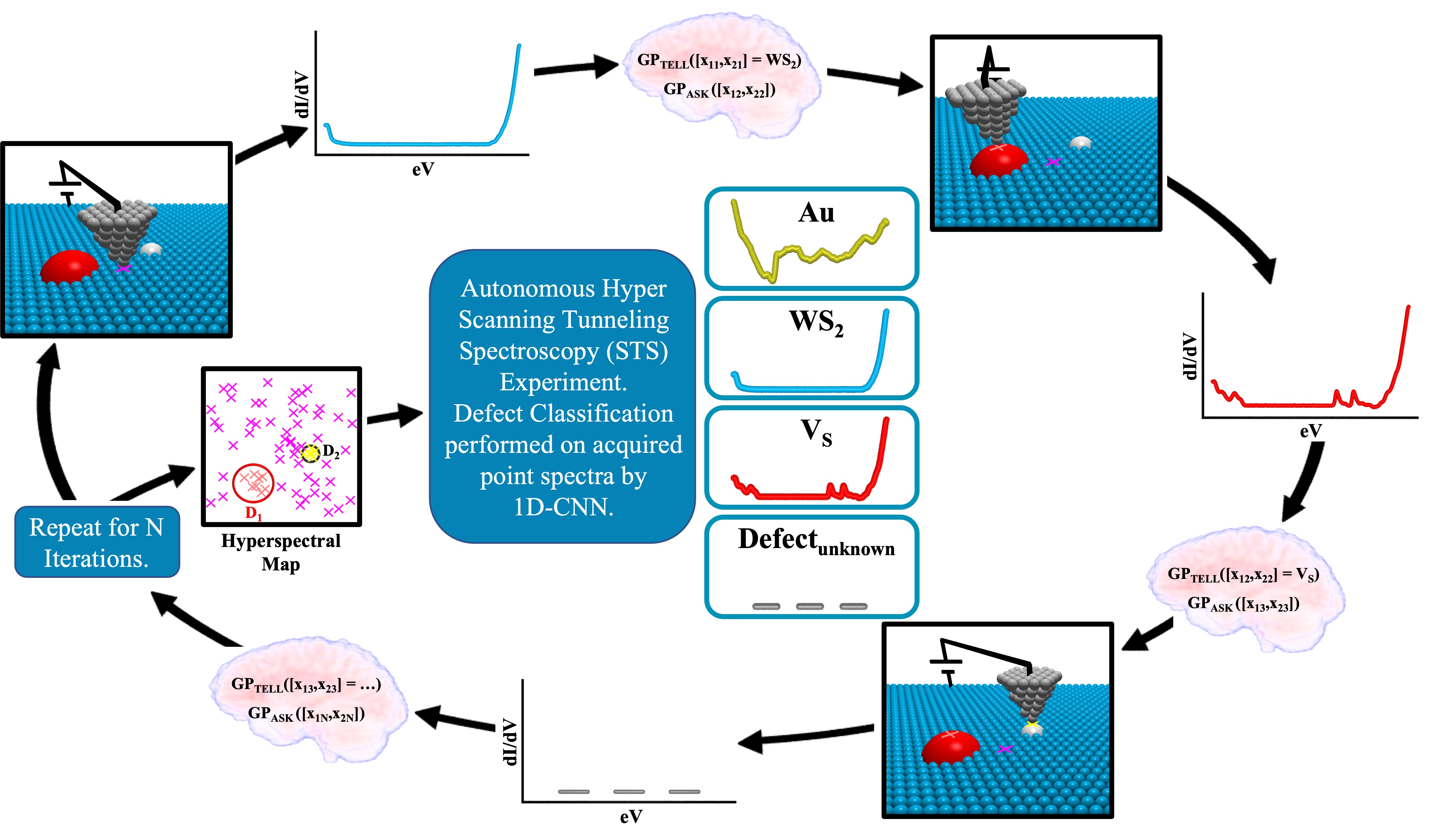
An autonomous hyperspectral STM/STS experiment can be initialized over any substrate that is either conducting or semi-conducting. Spatial parameters and tip offsets in both the - and - direction are defined by an input image (as defined by point locations and with y signal) that is further used in cross-correlation feature tracking (see Supplementary Notes 1-4). At each point defined by the GP, the bias is ramped over a certain voltage range while the tip is held at constant height. Each spectra can then be identified by a 1D-CNN, where class probabilities are computed, and the sum of dI/dV signal intensity is input into the GP for mean and objective function calculation. As the experiment progresses, a proposed measurement is given to the instrument to collect a point at the uncertainty maximum. A workflow summary of an autonomous experiment is presented in Figure 1, where an atomically sharp tip is directed to the next point for STS point acquisition by exploration that ultimately provides a 3D volume of data defined by both and , where is the current and is the voltage. The true power of this methodology is evident when sufficient orbital information (specific for the VS deep in-gap state within WS2) and surface structure details (over and ) can be obtained in well under 100 collected data points (close to 1% of the data compared to a CITS grid measurement) that is verified against ground truth data (see Supplementary Figures 1-6) to remove any conceivable bias across experiments, where signal intensity over a given voltage range is monitored.26, 11
A GP model can be defined for a given dataset, , where the regression model assumes , where x are the positions in some input or parameter space, is the associated noisy function evaluation, and represents the noise term. The variance-covariance matrix of the prior Gaussian probability distribution is defined via kernel functions , where is a set of hyperparameters that are found by maximizing the marginal log-likelihood of the data (earlier referred to as learning). The Matérn kernel is commonly used to match physical processes and is combined with an anisotropic kernel definition to control the level of differentiability in each direction of the input space.42 A predictive mean and variance can then be defined given a Gaussian probability distribution with a set of optimized hyperparameters, which can be further used to find the next optimal point measurements in the GP-driven data acquisition loop (see Supplementary Note 1). GP-driven autonomous experimentation (within the context of Bayesian optimization), where a statistical model of the system is generated based on prior data, uses an acquisition function to suggest the next point of input, which is non-trivial in its design. There are a number of acquisition functions available with different balances of exploration, with the goal to improve the statistical model, and exploitation, with the goal of utilizing the improved statistical model to find the global optimum.
Here experimental data is collected by exploration, where points are suggested to improve the Gaussian process via point selection at uncertainty maxima. The full energy range, which is defined by the accessible voltage range over a given sample that can represent a measurable band gap at both the valence band maximum and conduction band minimum or the range where representative surface states lie (as is the case for and Au, respectively), can be measured at each point, and indeed we can zoom into any voltage range to visualize orbital information and are able to obtain an optimized hyperspectral map with high resolution both spatially and energetically. In order to evaluate the performance with different user-defined acquisition functions, which either combine posterior mean and variance functions or make use of enabled information-theoretical entities, we perform hyperspectral oversampling on W. After an extended and feasibly-obtainable experiment over 30 hours, sufficient data points are collected and we can interpolate over 128128 pixel grid from acquired data, which is autonomously driven with n = 866 collected data points and shown in Supplementary Figure 1, and compare different acquisition functions using variance, Gaussian process upper confidence bound (GP-UCB), and Shannon’s information gain (SIG) (Supplementary Figures 2-6). Here we use a side-by-side comparison of a GP-driven experiment compared to standard grid methodologies, where the GP point acquisition determined by either variance, GP-UCB, or SIG all out perform comparable grid collections. We additionally show the performance of purely random collected data points (Supplementary Figure 3), where an experiment steered in this fashion shows performance degradation, and consistently and significantly requires more iterations versus a GP-driven CITS measurement (shown over n = 20 experiments). Across acquisition functions, the variance determined from the variance-covariance matrix shows a low of 30 and high of 79 iterations to reach 95% correlation, the UCB method shows a low of 27 and high of 74 iterations to reach this benchmark, and SIG shows a low of 25 and high of 74 iterations required ( = 54.2 14.7, = 53.1 12.4, = 50.0 13.2). Performing a one-way ANOVA analysis, we fail to reject the null hypothesis that the means are equal across acquisition functions, however, we do indeed reject the null hypothesis that means among a random experiment, variance, UCB, and Shannon’s information gain are equal ( << 0.05), which is driven by the elevation and subsequent mismatch of randomly-driven point acquisition.
3.2 Convolutional Neural Networks for Spectral Identification
When the sufficient data is collected, we can further successfully identify VS compared to pristine WS2 and distinguish versus with a trained 1D-CNN using an 80/20 train/test split ratio on 1482 individually and separately acquired scanning tunneling spectra, consisting of 424 , 709 , 158 , and 191 spectra (Figure 2). Test data is further split (60/40 ratio) into a validation set used during training to give an estimate of the model’s skill and a test set used on unbiased data after training. CNN architectures have shown application towards identifying tip state on H:Si(100),56 with automated hydrogen lithography,57, 58 in identifying adatom arrays on a cleaved surface,59 and to aid in automating carbon monoxide functionalization with use in noncontact atomic force microscopy.55 The CNN architecture chosen uses shared weights to reduce the number of trainable parameters and extract spectral features on the pixel level, which is based on hyperspectral image classification methods used on AVIRIS sensor datasets.60, 61
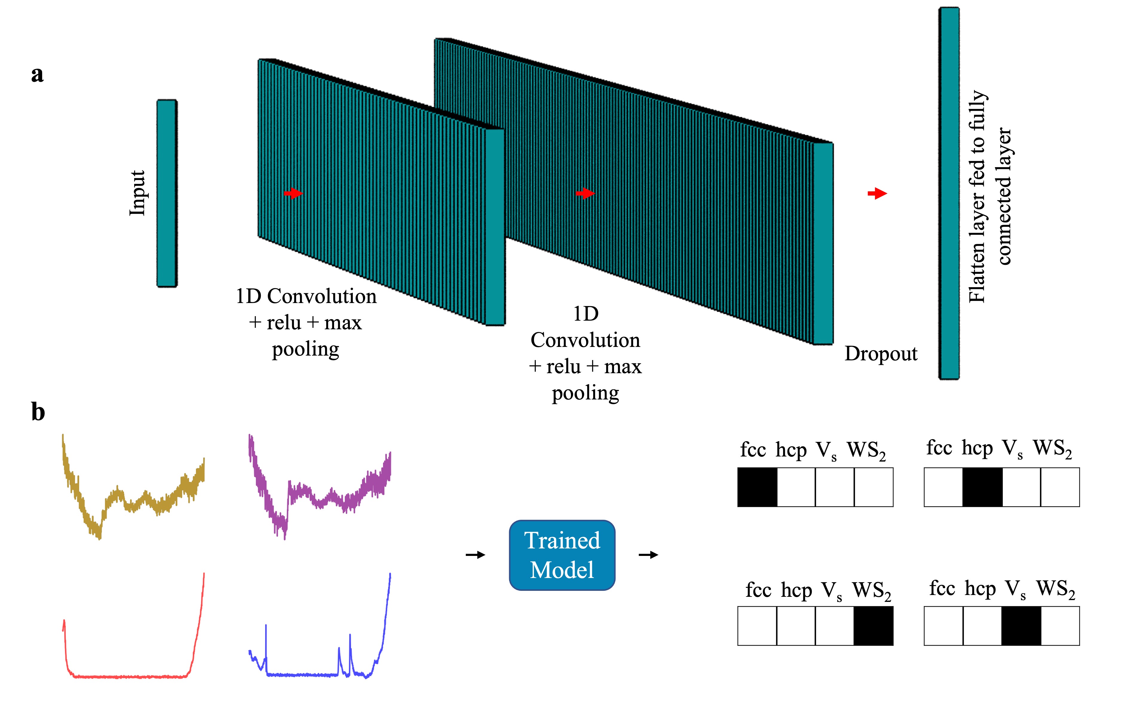
The 1D-CNN contains two convolution layers, one dropout layer to help overcome overfitting, and one fully connected linear layer, where the softmax can then be used after training to obtain point STS class probabilities. Each convolutional layer makes use of a 1x3 kernel to compute the sliding dot product and produce spectral feature maps at each layer (stride 1, padding 1), which is followed by batch normalization, a rectified linear unit (ReLU) activation, and maxpooling layer. The pooling layer down-samples each map while retaining the most important information. ReLU is a nonlinear operation that retains neuron values if it is positive or returns a zero if the input is negative, and is used on both 64 and 128 node layers. During training, the Adam algorithm62 with a learning rate of and computed cross-entropy loss for optimization are used to automatically identify spectral features, where the Adam optimizer minimizes loss. Input and output are shown in Figure 2, where spectra for , , , and that is unseen by the trained model is input and passed through the defined network to produce class identification. Accuracy and loss are further shown through 20 epochs for both training and test data (Supplementary Figure 7), with class accuracy scores presented in Table 1 for the first six epochs.
| Training | |||
| 63.2 | 49.5 | 43.6 | 64.5 |
| 98.1 | 98.8 | 93.3 | 97.6 |
| 98.8 | 99.6 | 99.4 | 100.0 |
| 95.9 | 98.5 | 97.8 | 98.2 |
| 100.0 | 99.8 | 100.0 | 99.5 |
| 100.0 | 100.0 | 100.0 | 100.0 |
| Validation | |||
| 100.0 | 24.1 | 0.0 | 100.0 |
| 95.6 | 98.9 | 95.7 | 100.0 |
| 100.0 | 96.6 | 100.0 | 100.0 |
| 88.9 | 100.0 | 100.0 | 100.0 |
| 95.6 | 100.0 | 100.0 | 100.0 |
| 95.6 | 100.0 | 100.0 | 100.0 |
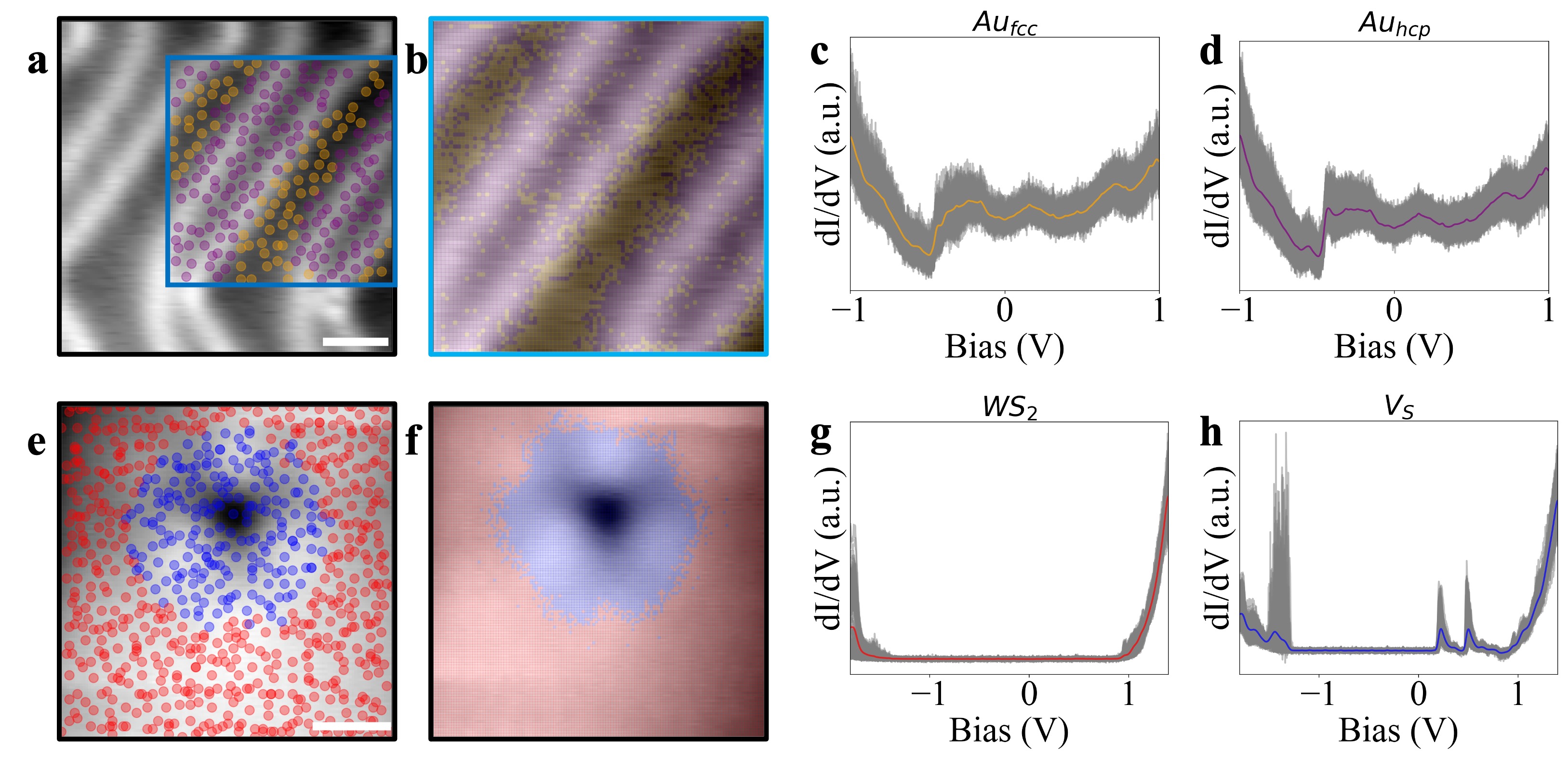
Pristine WS2, , Auhcp, and Aufcc training spectra are all optimized within the first 6 epochs, where the model reaches > 95% accuracy on Aufcc validation data after 5 epochs and 100% accuracy for remaining classes. Overall test performance reaches 100% accuracy after 6 epochs, which is the model chosen for classification (see Supplementary Figures 8-10 for test performance metrics). This paves the way for enabling reproducible STS over surface variations that are distinguishable via bias spectroscopy by providing class probabilities for operators to benchmark against, which can be further expanded to any relevant material. Subsequent identification over herringbone reconstruction is performed (Figure 3), where an impurity is used to track drift during a given cycle, dense hyperspectral data is classified with the 1D-CNN, and image segmentation can be performed with individually classed STS point overlays or pixel-by-pixel using an interpolated form. The peak in dI/dV at -0.48 V shows the tendency for low energy surface-state electrons to localize in Auhcp regions.11 A completed experiment over a within WS2 is also presented showing defect segmentation using the trained 1D-CNN. As most STM/STS data require high-quality tips and surfaces, the data acquired can be used to verify tip quality on both Au{111} and , however this is not explicitly explored within the methods presented.
3.3 Autonomous Experimentation
Experiments are performed at liquid helium temperatures and in ultrahigh vacuum to minimize any drift during an experimental run. A number of drift correction techniques have been explored, which take advantage of machine vision techniques, feature tracking, atom-tracking, image pairs, or thermal drift correction methodologies, to list some of the approaches within the literature.63, 64, 65, 66, 67 To correct for any residual drift, driven by either thermal fluctuations during piezo motion, sample-to-sample variability, or any tool-to-tool difference, we acquire interval images at a predefined offset window and then compute feature correlation (between spectral acquisition and after n = 10 points) using sliding image patches (Supplementary Figure 11). This block-matching approach is a common technique for image recognition and operates by taking the maximum correlation within a given pixel range.68, 69, 70 Any computed offset is registered to the tool by updating the scan window location during the autonomous hyperspectral experiment. Collected images are plane corrected with a line-by-line linear fit to adjust for tilt, since SPM tips are not always perfectly normal to a given sample. Each high resolution spectra is swept from +1.4 V to -1.8 V on WS2 (or +1 to -1 V on Au) and takes 2 minutes for the complete sweep. After two completed autonomous experiments, drift was measured to be on the order of 0.5 0.2 Å on WS2 and 1.1 0.8 Å over Au{111} that is shown in Supplementary Figure 12. Hyperparameters can be fine-tuned to best accommodate for any of the defined drift modes during an experiment and for subsequent reproducibility.
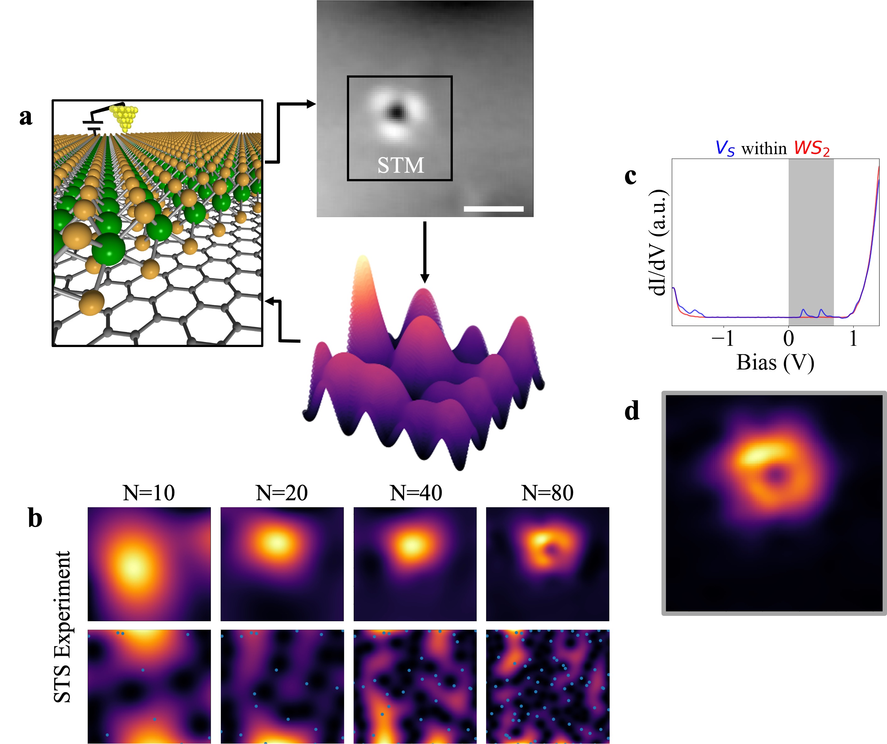
Hyperparameters for both prior-mean model and covariance functions can be optimized after each point acquired during an autonomous experiment. We further show a summary example in Figure 4, depicting the progression of such an experiment in the case of a within WS2, where the user defines the measurement space by providing a topographic image to the software and uncertainty is extracted after every point acquired to determine the next point of acquisition (further detailed in Supplementary Figure 13). The means to direct measurements, optimize a grid, and decrease the time required for sample scrutiny is of key importance within the materials discovery and scanning probe fields, where high-resolution point spectroscopy is on the order of minutes and capturing a dense 128128 grid with zero drift isn’t feasible with available systems (0.14 days with GP compared to 22.76 days for a dense CITS measurement). Enhanced experimental throughput with such a method provides an additional tool for users to collect and identify defects without human bias and/or intervention.
4 Discussion
A method for autonomous experimentation is presented that makes use of both GPs and a 1D-CNN for spectral identification, which enables point defect fingerprinting across a wide variety of materials and surfaces. Image segmentation can be subsequently executed after spectral classification. As experiments can be performed without time-intensive input from the operator and at a lower spatial density, high resolution STM/STS can be performed in an autonomous fashion allowing for less redundant information over a given area of interest. Additionally, as neural network algorithms tend to require a large amount of data, the GP can be operated in exploration mode for an increased number of observations to contribute towards statistically significant measurements and ML training on, e.g., an uninvestigated system of interest with spectroscopic signatures not readily available in the literature. The methods presented make use of spectroscopically variant features within a material, where a user can collect data directed by uncertainty quantification or any preferred acquisition function, and use classification to determine tip quality or train on a defined number of classes. We expect that the open source software package can find application across the scanning probe field and greatly increase experimental efficiency, where the library can be easily extended to any system accessible with STM/STS.
Where previous reports have used either spatial features, decreased pixel density in spectral space, or some combination for segmentation and CITS measurements with an STM, we unambiguously identify defects and surface-state based on high resolution spectral features that leverage the power of Gaussian processes combined with a CNN architecture for prediction. This hyperspectral STS mapping measurement technique that combines CITS with AI/ML enables full characterization of heterogeneous sample surfaces, ensuring that no local spectral features are missed, even by a non-experienced user.
5 Methods
5.1 Scanning probe microscopy (SPM) measurements
All measurements were performed with a Createc GmbH scanning probe microscope operating under ultrahigh vacuum (pressure < 2x mbar) at liquid helium temperatures (T < 6 K). Either etched tungsten or platinum iridium tips were used during acquisition. Tip apexes were further shaped by indentations onto a gold substrate. STM images are taken in constant-current mode with a bias applied to the sample. STS measurements were recorded using a lock-in amplifier with a resonance frequency of 683 Hz and a modulation amplitude of 5 mV.
5.2 Sample Preparation
Monolayer islands of WS2 were grown on graphene/SiC substrates with an ambient pressure CVD approach. A graphene/SiC substrate with 10 mg of WO3 powder on top was placed at the center of a quartz tube, and 400 mg of sulfur powder was placed upstream. The furnace was heated to 900 ∘C and the sulfur powder was heated to 250 ∘C using a heating belt during synthesis. A carrier gas for process throughput was used (Ar gas at 100 sccm) and the growth time was 60 min. The CVD grown /MLG/SiC was annealed in vacuo at 600 ∘C for 30 minutes to induce sulfur vacancies.
5.3 Neural Network and Gaussian Process Implementation
The acquisition software provided leverages the integration of Python and LabVIEW, and makes use of the Nanonis programming interface. The GP was implemented using gpCAM, which is a library for autonomous experimentation by M. M. Noack.71 The CNN was constructed with Pytorch, which is a deep-learning library available in Python. An Intel Xeon E5-2623 v3 CPU with 8 cores and 64 GB of memory combined with a Tesla K80 with 4992 CUDA cores was used for training.
Data availability
All data needed to evaluate the conclusions exhibited are present in the paper, supplemental information, and/or available on zenodo (https://doi.org/10.5281/zenodo.5768320).
Code availability
The full suite of home-built software is available at https://github.com/jthomas03/gpSTS.
Acknowledgments
This work was supported as part of the Center for Novel Pathways to Quantum Coherence in Materials, an Energy Frontier Research Center funded by the U.S. Department of Energy, Office of Science, Basic Energy Sciences. Work was performed at the Molecular Foundry supported by the Office of Science, Office of Basic Energy Sciences, of the U.S. Department of Energy under contract no. DE-AC02-05CH11231. Work was also funded through the Center for Advanced Mathematics for Energy Research Applications (CAMERA), which is jointly funded by the Advanced Scientific Computing Research (ASCR) and Basic Energy Sciences (BES) within the Department of Energy’s Office of Science, under Contract No. DE-AC02-05CH11231. S.K and J.A.R. acknowledge support from the National Science Foundation Division of Materials Research (NSF-DMR) under awards 2002651 and 2011839. L.F. acknowledges funding from the Swiss National Science Foundation (SNSF) via Early PostDoc Mobility Grant no. P2ELP2_184398.
Author Contributions
J.C.T., A.R., D.S., L.F., M.I., E.R., E.S.B., A.R., M.M.N., and A.W.-B. contributed to data analysis, neural network development, and software implementation. Z.Y., T.Z., S.K., J.A.R., and M.T. synthesized the samples. J.C.T, A.R., E.W., D.F.O., and A.W.-B. helped perform STM measurements and setup experiments. All authors discussed the results and contributed towards the manuscript.
Competing interests
The authors declare that they have no competing interests.
References
- 1 Stern, H. L. et al. Room-temperature optically detected magnetic resonance of single defects in hexagonal boron nitride. Nat. Commun. 13, 618 (2022).
- 2 Kianinia, M., Xu, Z.-Q., Toth, M., & Aharonovich, I. Quantum emitters in 2d materials: Emitter engineering, photophysics, and integration in photonic nanostructures. Appl. Phys. Rev. 9 011306 (2022).
- 3 Zhang, X. et al. Electron spin resonance of single iron phthalocyanine molecules and role of their non-localized spins in magnetic interactions. Nat. Chem. 14, 59-65 (2022).
- 4 Lin, Z. et al. Defect engineering of two-dimensional transition metal dichalcogenides. 2D Mater. 3 022002 (2016).
- 5 Sangwan, V. K. & Hersam, M. C. Electronic transport in two-dimensional materials. Annu. Rev. Phys. Chem. 69 299-325 (2018).
- 6 Shimazaki, Y. et al. Strongly correlated electrons and hybrid excitons in a moiré heterostructure. Nature 580 472-477 (2020).
- 7 Wang, L. et al. Correlated electronic phases in twisted bilayer transition metal dichalcogenides. Nat. Mater. 19 861-866 (2020).
- 8 Zandvliet, H. J. W. & van Houselt, A. Scanning tunneling spectroscopy. Annu. Rev. Anal. Chem. 2 37-55 (2009).
- 9 Hamers, R. J. Atomic-resolution surface spectroscopy with the scanning tunneling microscope. Annu. Rev. Phys. Chem. 40 531-559 (1989).
- 10 Peng, W. et al. Recent progress on the scanning tunneling microscopy and spectroscopy study of semiconductor heterojunctions. Small 17 e2100655 (2021).
- 11 Chen, W., Madhavan, V., Jamneala, T., & Crommie, M. F. Scanning tunneling microscopy observation of an electronic superlattice at the surface of clean gold. Phys. Rev. Lett. 80 1469-1472 (1998).
- 12 Weber-Bargioni, A. et al. Hyperspectral nanoscale imaging on dielectric substrates with coaxial optical antenna scan probes. Nano Lett., 11 1201-1207 (2011).
- 13 Dong, X. et al. A review of hyperspectral imaging for nanoscale materials research. Appl. Spectrosc. Rev. 54 285-305 (2019).
- 14 Bannon, D. Cubes and slices. Nat. Photonics 3 627-629 (2009).
- 15 Ophus, C. Four-dimensional scanning transmission electron microscopy (4D-STEM): From scanning nanodiffraction to ptychography and beyond. Microsc. Microanal. 25 563–582 (2019).
- 16 Novotny, Z., Zhang, Z., & Dohnálek, Z. Imaging chemical reactions one molecule at a time. In Encyclopedia of Interfacial Chemistry 220-240 (Elsevier, 2018).
- 17 Stipe, B. C., Rezaei, M. A., & Ho, W. Single-molecule vibrational spectroscopy and microscopy. Science 280 1732-1735 (1998).
- 18 Jelic, V. et al. Ultrafast terahertz control of extreme tunnel currents through single atoms on a silicon surface. Nat. Phys. 13 591-598 (2017).
- 19 Garg, M. & Kern, K. Attosecond coherent manipulation of electrons in tunneling microscopy. Science 367 411-415 (2020).
- 20 Kimura, K. et al. Terahertz-field-driven scanning tunneling luminescence spectroscopy. ACS Photonics 8 982-987 (2021).
- 21 Barja, S. et al. Identifying substitutional oxygen as a prolific point defect in monolayer transition metal dichalcogenides. Nat. Commun. 10 3382 (2019).
- 22 Wang, S., Robertson, A., & Warner, J. H. Atomic structure of defects and dopants in 2D layered transition metal dichalcogenides. Chem. Soc. Rev. 47 6764-6794 (2018).
- 23 Srivastava, A. et al. Optically active quantum dots in monolayer W. Nat. Nanotechnol. 10 491-496 (2015).
- 24 Schuler, B. et al. How substitutional point defects in Two-Dimensional W induce charge localization, Spin-Orbit splitting, and strain. ACS Nano 13 10520-10534 (2019).
- 25 Schaibley, J. R. et al. Valleytronics in 2D materials. Nat. Rev. Mater. 1 1-15 (2016).
- 26 Schuler, B. et al. Large Spin-Orbit splitting of deep in-gap defect states of engineered sulfur vacancies in monolayer W. Phys. Rev. Lett. 123 076801 (2019).
- 27 Manzeli, S., Ovchinnikov, D., Pasquier, D., Yazyev, O. V. & Kis, A. 2D transition metal dichalcogenides. Nat. Rev. Mater. 2 1-15 (2017).
- 28 Liu, K. et al. Evolution of interlayer coupling in twisted molybdenum disulfide bilayers. Nat. Commun. 5 4966 (2014).
- 29 Li, C. et al. Engineering graphene and TMDs based van der waals heterostructures for photovoltaic and photoelectrochemical solar energy conversion. Chem. Soc. Rev. 47 4981-5037 (2018).
- 30 Mitterreiter, E. et al. Atomistic positioning of defects in helium ion treated single-layer Mo. Nano Lett. 20 4437-4444 (2020).
- 31 Mitterreiter, E. et al. The role of chalcogen vacancies for atomic defect emission in Mo. Nat. Commun. 12 3822 (2021).
- 32 Schuler, B. et al. Electrically driven photon emission from individual atomic defects in monolayer W. Sci. Adv. 6 eabb5988 (2020).
- 33 Claridge, S. A. et al. From the bottom up: dimensional control and characterization in molecular monolayers. Chem. Soc. Rev. 42 2725-2745 (2013).
- 34 Laibinis, P. E. et al. Comparison of the structures and wetting properties of self-assembled monolayers of n-alkanethiols on the coinage metal surfaces, copper, silver, and gold. J. Am. Chem. Soc. 113 7152-7167 (1991).
- 35 Ellis, T. W. The future of gold in electronics. Gold Bull. 37 66-71 (2004).
- 36 Shirai, Y., Cheng, L., Chen, B., & Tour, J. M. Characterization of self-assembled monolayers of fullerene derivatives on gold surfaces: implications for device evaluations. J. Am. Chem. Soc. 128 13479-13489 (2006).
- 37 Asenjo, A., Gómez-Rodríguez, J. M., & Baró, A.M. Current imaging tunneling spectroscopy of metallic deposits on silicon. Ultramicroscopy 42-44 933-939 (1992).
- 38 Cochrane, K. A. et al. Spin-dependent vibronic response of a carbon radical ion in two-dimensional W. Nat. Commun. 12 7287 (2021).
- 39 Noack, M. M. et al. Gaussian processes for autonomous data acquisition at large-scale synchrotron and neutron facilities. Nat. Rev. Phys. 3 685-697 (2021).
- 40 Melton, C. N. et al. K-means-driven gaussian process data collection for angle-resolved photoemission spectroscopy. Mach. Learn. Sci. Technol. 1 045015 (2020).
- 41 Ziatdinov, M. et al. Imaging mechanism for hyperspectral scanning probe microscopy via gaussian process modelling. NPJ Comput. Mater. 6 1-7 (2020).
- 42 Williams, C. K. & Rasmussen, C. E. Gaussian processes for machine learning. (MIT Press, 2006).
- 43 Noack, M. M. et al. Autonomous materials discovery driven by gaussian process regression with inhomogeneous measurement noise and anisotropic kernels. Sci. Rep. 10 17663 (2020).
- 44 Borodinov, N. et al. Deep neural networks for understanding noisy data applied to physical property extraction in scanning probe microscopy. NPJ Comput. Mater. 5 25 (2019).
- 45 Nyshadham, C. et al. Machine-learned multi-system surrogate models for materials prediction. NPJ Comput. Mater. 5 51 (2019).
- 46 Saal, J. E., Oliynyk, A. O. & Meredig, B. Machine learning in materials discovery: Confirmed predictions and their underlying approaches. Annu. Rev. Mater. Res. 50 49-69 (2020).
- 47 Vasudevan, R. K., Ziatdinov, M., Vlcek, L., & Kalinin, S. V. Off-the-shelf deep learning is not enough, and requires parsimony, bayesianity, and causality. NPJ Comput. Mater. 7 16 (2021).
- 48 Vasudevan, R. K. et al. Autonomous experiments in scanning probe microscopy and spectroscopy: Choosing where to explore polarization dynamics in ferroelectrics. ACS Nano 15 11253-11262 (2021).
- 49 Brown, K. A., Brittman, S., Maccaferri, N., Jariwala, D., & Celano, U. Machine learning in nanoscience: Big data at small scales. Nano Lett. 20 2-10 (2020).
- 50 Kalinin, S. V. et al. Automated and autonomous experiment in electron and scanning probe microscopy. ACS Nano 15 12604-12627 (2021).
- 51 Gordon, O. M. & Moriarty, P. J. Machine learning at the (sub)atomic scale: next generation scanning probe microscopy. Mach. Learn. Sci. Technol. 1 023001 (2020).
- 52 Leinen, P. et al. Autonomous robotic nanofabrication with reinforcement learning Sci. Adv. 6 eabb6987 (2020).
- 53 Azuri, I., Rosenhek-Goldian, I., Regev-Rudzki, N., Fantner, G., & Cohen, S. R. The role of convolutional neural networks in scanning probe microscopy: a review. Beilstein J. Nanotechnol. 12 878-901 (2021).
- 54 Sotres, J., Boyd, H., & Gonzalez-Martinez, J. F. Enabling autonomous scanning probe microscopy imaging of single molecules with deep learning. Nanoscale 13 9193-9203 (2021).
- 55 Alldritt, B. et al. Automated tip functionalization via machine learning in scanning probe microscopy. Comput. Phys. Commun. 273 108258 (2022).
- 56 Rashidi, M. & Wolkow, R. A. Autonomous scanning probe microscopy in situ tip conditioning through machine learning. ACS Nano 12 5185-5189 (2018).
- 57 Rashidi, M. et al. Deep learning-guided surface characterization for autonomous hydrogen lithography. Mach. Learn. Sci. Technol. 1 025001 (2020).
- 58 Krull, A., Hirsch, P., Rother, C., Schiffrin, A., & Krull, C. Artificial-intelligence-driven scanning probe microscopy. Commun. Phys. 3 1-8 (2020).
- 59 Roccapriore, K. M. et al. Revealing the chemical bonding in adatom arrays via machine learning of hyperspectral scanning tunneling spectroscopy data. ACS Nano 15 11806-11816 (2021).
- 60 Miclea, A. V., Terebes, R., & Meza, S. One dimensional convolutional neural networks and local binary patterns for hyperspectral image classification. In 2020 IEEE International Conference on Automation, Quality and Testing, Robotics (AQTR). 1-6 (2020).
- 61 Ortac, G. & Ozcan, G. Comparative study of hyperspectral image classification by multidimensional convolutional neural network approaches to improve accuracy. Expert Syst. Appl. 182 115280 (2021).
- 62 Kingma, D. P. & Ba, J. Adam: A method for stochastic optimization. Preprint at https://arxiv.org/abs/1412.6980 (2014).
- 63 Rahe, P., Bechstein, R., & Kühnle, A. Vertical and lateral drift corrections of scanning probe microscopy images. J. Vac. Sci. Technol. B 28 C4E31-C4E38 (2010).
- 64 Ophus, C., Ciston, J., & Nelson, C. T. Correcting nonlinear drift distortion of scanning probe and scanning transmission electron microscopies from image pairs with orthogonal scan directions. Ultramicroscopy 162 1-9 (2016).
- 65 Swartzentruber, B. S. Direct measurement of surface diffusion using atom-tracking scanning tunneling microscopy. Phys. Rev. Lett. 76 459-462 (1996).
- 66 Mantooth, B. A. et al. Analyzing the motion of benzene on Au111: single molecule statistics from scanning probe images. J. Phys. Chem. C 111 6167-6182 (2007).
- 67 Gaponenko, I. et al. Computer vision distortion correction of scanning probe microscopy images. Sci. Rep. 7 669 (2017).
- 68 Thomas, J. C. et al. Defect-tolerant aligned dipoles within two-dimensional plastic lattices. ACS Nano 9 4734-4742 (2015).
- 69 Jain, J. & Jain, A. Displacement measurement and its application in interframe image coding. IEEE Trans. Commun. 29 1799-1808 (1981).
- 70 Love, N. & Kamath, C. An empirical study of block matching techniques for the detection of moving objects. Tech. Rep. UCRL - TR - 218038, University of California, Lawrence Livermore National Laboratory (2006).
- 71 Noack, M. M. et al. gpCAM. https://github.com/lbl-camera/gpCAM (2022).