Now at ]Oxford Instruments Nanoscience, Abingdon, Oxfordshire OX13 5QX, UK. Now at ]Department of Physics, Imperial College London, London SW7 2AZ, UK. Now at ]Thomas J. Watson Research Center, Yorktown Heights, NY 10598, USA. Now at ]Praesto Consulting, Dublin, D02 A342, Ireland. Now at ]Department of Electronic and Electrical Engineering, University of Sheffield, Sheffield S1 3JD, UK.
Cooling Low-Dimensional Electron Systems into the Microkelvin Regime
Abstract
Two-dimensional electron gases (2DEGs) with high mobility, engineered in semiconductor heterostructures host a variety of ordered phases arising from strong correlations, which emerge at sufficiently low temperatures. The 2DEG can be further controlled by surface gates to create quasi-one dimensional systems, with potential spintronic applications. Here we address the long-standing challenge of cooling such electrons to below 1 mK, potentially important for identification of topological phases and spin correlated states. The 2DEG device was immersed in liquid 3He, cooled by the nuclear adiabatic demagnetization of copper. The temperature of the 2D electrons was inferred from the electronic noise in a gold wire, connected to the 2DEG by a metallic ohmic contact. With effective screening and filtering, we demonstrate a temperature of 0.90.1 mK, with scope for significant further improvement. This platform is a key technological step, paving the way to observing new quantum phenomena, and developing new generations of nanoelectronic devices exploiting correlated electron states.
I Introduction
Two-dimensional electron gases (2DEGs), created at a GaAs-AlGaAs heterojunction and grown by molecular-beam epitaxy (MBE), have been the building block for the study of low-dimensional physics over the past few decades. This requires the high crystal perfection of MBE growth and the use of modulation doping (see Ref. [1] for a review of the state of the art).
The lowest possible electron carrier temperature coupled to the highest sample quality is key to discovering and elucidating new ground states in such systems. The observation of the integer quantum Hall effect [2] and shortly thereafter the fractional quantum Hall effect (FQHE) [3] has led to extensive studies of two-dimensional electron systems in perpendicular magnetic field . The lowest Landau level (LL), with filling factors (here is determined by the carrier density , Planck’s constant and elementary charge ) for the lowest spin branch is described by composite fermion (CF) theory [4]. It exhibits a rich variety of quantum states: fractional quantum Hall states for odd fractions, while is a composite fermion Fermi sea [5]. A key question is the role of residual CF interactions in giving rise to exotic states [6]. A Wigner solid is found for small , which also exhibits re-entrance with a maximum melting temperature of 50 mK above the FQHE state [7]. Interactions are also believed to play a role at other fractional fillings such as , which has a measured activation energy of 5 mK [8].
The nature of quantum states in the second LL is in many cases not resolved, and this 2D electron system is of particular interest for study to lower temperatures than hitherto achieved. We discuss a few examples here. Even denominator states forming in the second Landau level are thought to arise from pairing of composite fermions. Confirmation of exact quantization of the 5/2 state first discovered by Willett et al. [9] required electron temperatures as low as 8 mK [10]. Nevertheless the topology of the ground state (Pfaffian, anti-Pfaffian or other) remains an open question. Observations are highly sensitive to disorder [11, 12]. It has been shown that a quantum phase transition to a quantum Hall nematic phase can be induced by applied pressure in both the 5/2 and 7/2 state [13]. The importance of such topological ground states is reinforced by the proposal that they offer a route to topological quantum computing using non-Abelian anyons [14]. A non-Abelian phase is also predicted for the 12/5 state.
Many of these states have small energy gaps. The 12/5 state has a gap of order 30 mK, which exhibits non-trivial tilt dependence of the magnetic field. Studies of the energy gaps at other fractional fillings [15, 16] found that the gaps of the (10 mK) and (80 mK) states do not follow the CF hierarchy, leading to the proposal of a parton state [17]. The state also has a reported gap of only 10 mK. Furthermore there are indications of novel topological order in the upper spin branch of the second LL, at fillings (37 mK) and (104 mK) [18].
New states arising from strong correlations in the low-dimensional electron system are also expected in low magnetic fields. Electrostatic confinement of the 2DEG to form 1D wires and zero-dimensional (0D) quantum dots has led to studies of the many-body physics of Luttinger liquids [19, 20] and the Kondo effect [21, 22]. Furthermore the conduction electrons in GaAs-based 2DEGs are expected to couple to the nuclear spins, undergoing a collective ferromagnetic transition mediated by RKKY interactions which is expected at electron temperatures in the mK regime [23]. The hyperfine interaction is also predicted [24] to create new topological phases in a semiconductor 1D wire coupled to a superconductor and magnetic moments. A transition from metal- to insulator-like behaviour with decreasing temperature has been reported in a 2D hole gas in GaAs [25], potentially related to many-body localization. Recently, Wigner crystal-like zigzag chains have been discovered in 1D wires at low electron densities [26]. At lower temperatures there is potential for of quantum communication through 1D spin chains, coupling high fidelity quantum dot qubits [27].
Advances in cryogen-free technologies now make low millikelvin temperature platforms widely accessible [28], with prospects of commercial solutions in the microkelvin range [29, 30]. However cooling electrons in semiconductor devices is challenging. In situ cooling via the electron-phonon coupling is severely limited by its strong temperature dependence, while the electrons are susceptible to heat leaks arising from electromagnetic noise. Electromagnetic shielding and ultra-sensitive measurement schemes with low or no electrical excitation [31, 32, 33] are common strategies for minimising the heat leak. Cooling via the electrical leads has been widely implemented [33, 34, 10, 35, 36], commonly employing immersion in liquid helium. For 2D electrons, this has so far been limited, for many years, to 4 mK, see Ref. [34] and references therein. Primary thermometers within samples confirmed 2D electron temperatures of 6 mK [33, 36].
In response to the challenge to cool nano-electronic devices to ultra-low temperatures (ULT), new approaches have been introduced which focus on refrigeration by nuclear demagnetisation of each lead connected to the sample [39]. More recently this has been extended by incorporating nuclear refrigeration elements into the device itself. For this on-chip cooling the Coulomb blockade device used is itself a thermometer, providing an accurate measurement of the electron temperature in mesoscopic metallic islands as low as 0.5 mK [40, 41].
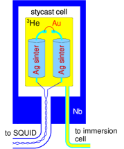
In contrast, and complementary to this approach, the focus of our work is the cooling of a relatively large area (8 mm2) 2DEG. Our approach to cooling is motivated by the requirement for flexibility to cool a wide range of devices in different sample environments. We report an ultimate electron temperature in the 2DEG of mK, cooled in a 3He immersion cell, achieved after improvements in electromagnetic shielding. The 2DEG device is immersed in liquid 3He and cooled through metallic ohmic contacts, which are coupled to the 3He via compact heat exchangers made of sintered Ag powder. Cooling of devices by the immersion cell technique, as compared to on-chip cooling, is remarkably versatile due to modularity of the design. The cooling is provided by a physically remote copper nuclear adiabatic demagnetization stage module, so the magnetic field applied to the sample can be independently adjusted. A broad class of devices can potentially be cooled in this way, and in some cases the 3He liquid pressure can be used as an experimental control parameter [42].
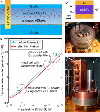
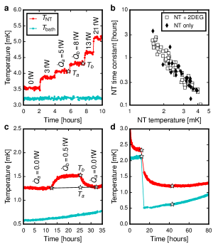
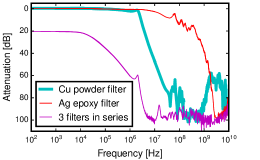
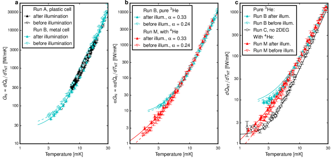
The effective cooling of electrons in the 2DEG relies on both reducing the resistance (and hence thermal resistance via the Wiedemann-Franz law) of the 2DEG and ohmic contacts, and reducing the heat leak to the device. We fabricated a high-mobility GaAs-based 2DEG with sub- AuNiGe ohmic contacts, see Fig. 1a,b, and reached a 1 fW level of heat leak to the 2DEG, see Fig. 1c, through designing a metal cell that is tight to photons over a wide frequency range, combined with extensive filtering of all electrical lines, see Fig. 2.
A key feature of the experiment was the choice of thermometer. We use a current sensing noise thermometer (NT) as an external module attached to the 2DEG via an ohmic contact. A SQUID current sensor is used to read out the voltage fluctuations across a gold wire [43]. Due to the fundamental Nyquist relation the NT operates over 5 orders of magnitude in temperature with a single point calibration. It can be configured as a primary thermometer [44], and as such underpins the recent redefinition of the Kelvin.
The noise thermometer dissipates no power in the device, but we must take account of both the inevitable residual heat leak into the thermometer, and the potential parallel cooling channel by direct coupling to the 3He in which it is immersed. We have constructed a thermal model which demonstrates that at the lowest temperatures the NT accurately reflects the electron temperature in the 2DEG. The ability to alter the resistance of the 2DEG in situ by optical illumination, due to persistent photoconductivity, was used to experimentally validate the model.
II Results
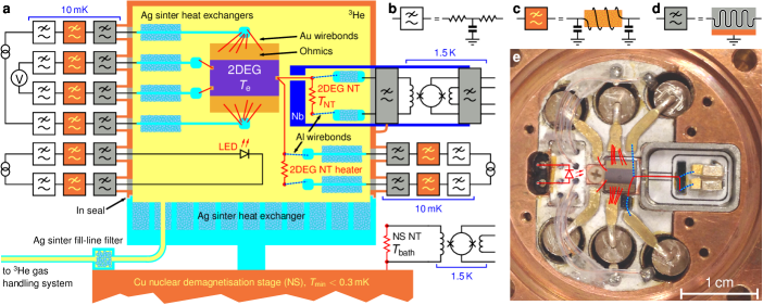
Experimental setup. Figure 2a is a schematic of the metal immersion cell, which combines a 3He bath with a photon-tight environment. Filtered connections to room-temperature electronics are provided to probe electrical resistances in the device and to operate heaters in thermal transport experiments. Two NTs are connected to the 2DEG and the demagnetisation refrigerator. Illumination by a red light-emitting diode (LED) facing the 2DEG allows us to increase the 2D carrier density and mobility [45]. Preliminary studies were conducted in a plastic cell shown in Fig. 1d, which was based on Ref. [34]. See Supplementary Information (SI) for further details.
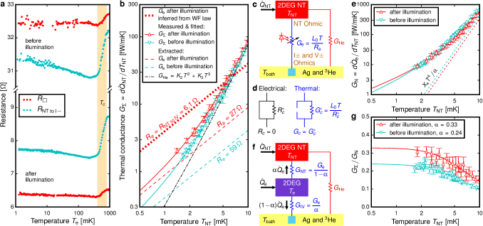
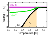
Electrical transport measurements. Figure 3a shows that the resistance of both the 2DEG and ohmic contacts exhibit a weak temperature dependence. These transport measurements were performed down to 1 mK with no discernible heating using conventional room temperature electronics without a screened room; this demonstrates the effectiveness of the filtering. A change in the resistance was observed between 0.4 and 0.8 K, that has been identified in similar samples [46] to be a superconducting transition in the ohmic contacts.
Thermal transport measurements and thermal model. The use of an external thermometer in our setup requires an investigation of the heat flow in the system in order to relate the electron temperature in the 2DEG to the 2DEG NT temperature . We consider two sources of heat: applied to the NT and uniformly generated within the 2DEG device. Each includes a residual heat leak ( and ); additionally, to study the thermal response Joule heating is applied using the NT heater and by driving a current between I and I ohmic contacts.
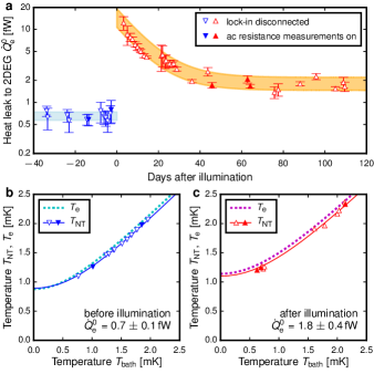
Figure 3b shows the thermal conductance between the 2DEG NT and the 3He bath, as inferred from measurements of as a function of at a constant 3He bath temperature . Figure 3c illustrates the two parallel channels of , via electrons in the 2DEG and ohmic contacts, and the Kapitza boundary conductance between the NT assembly and the 3He bath [47]. The illumination of the 2DEG increases , allowing us to separate it from . To reduce the heat exchangers in the immersion cell were plated with approx. 30 mol/m2 4He coverage before loading 3He [48].
In the initial stage of this research we assumed that both the 2DEG and the ohmic contacts obey the Wiedemann-Franz (WF) law, ubiquitous in electronic transport in the limit [49, 50, 51, 52, 53, 54]. The WF law predicts that , where is the electrical resistance from the NT ohmic contact to I and V connected in parallel, measured before (after) illumination, where is the Lorenz number [49]. Figure 3b shows that after illumination, a clear violation of the WF law that we attribute to superconductivity [55] in the ohmic contacts [46]. To the leading order the change in due to illumination is ; to explain this observation we propose a model of partially-superconducting ohmic contacts, see Fig. 3d, such that well below the superconducting transition temperature , is described by a resistance . The data are well described by
| (1) |
with () before (after) illumination and illumination-independent . Similarly the response to was characterised in terms of the non-local thermal conductance , see Fig. 3e, which was found to follow
| (2) |
with an illumination-independent term , but with different values of before and after illumination. The term describes an additional cooling mechanism in the 2DEG or ohmic contacts, insignificant below mK, where . In this low temperature regime, Eq. (2) reduces to where is the fraction of that flows towards the NT ohmic contact, as shown in Figs. 3f,g. Then
| (3) |
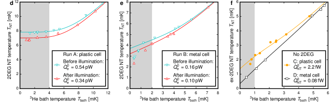
The combined heat leak can be inferred from the difference between and in the absence of Joule heating. We assume to be equal to the fridge temperature, as justified in SI. By replacing the gold thermal link between the NT ohmic contact and the NT with an aluminium one, we measured fW in a separate experiment (see SI), allowing us to obtain directly, see Fig. 4a. Before illumination by the LED the heat leak was found to be fW. After illumination there was a dramatic increase of followed by a slow relaxation, consistent with slow recombination processes in the heterostructure [56]. On a time scale of a month, a new stable level fW was reached, higher than before the illumination.
To estimate the minimum electron temperature in the 2DEG we use the simple model shown in Fig. 3f, in which is a point source of heat in the middle of the device and additional cooling associated with the term in Eq. (2) is ignored:
| (4) |
Figures 4b and c show the inferred electron temperature , demonstrating that we have cooled the electrons to 1 mK, despite the unexpected hindrance posed by the superconductivity in the ohmic contacts.
III Discussion
We demonstrate that at 1 mK the dominant cooling of the 2D electrons is by the ohmic contacts, which have a thermal conductance of W/K. The electron-phonon coupling in high-mobility 2DEGs has been observed [57] to follow eV/s K at phonon temperatures of -0.5 K, where is the number of electrons. For our device this leads to a thermal conductance W/K. Assuming this high-temperature power law extrapolates to ULT, the cross-over occurs near 100 mK and at 1 mK , so cooling via electron-phonon coupling alone would only achieve mK (70 mK) for mK and fW (500 fW).
The term in Eq. (2) points towards an additional cooling channel competing with above 3 mK, such as enhanced W/K at ULT; alternatively , and , see Fig. 3f, may deviate from the behaviour, if the effective contact resistance (see Fig. 3d) is not constant at ULT. Ignoring these effects in Eq. (4) potentially overestimates for the preliminary experiments shown in Fig. 1c, but the ultimate electron temperature we report and the qualitative observation of the reduction of the heat leak due to the electromagnetic shielding are robust. In addition to the term, a more detailed thermal model, beyond the scope of this work, should take into account the distribution of across the 2DEG and 2D and 3D heat flow in the 2DEG and ohmic contacts.
We note that after illumination the thermal resistances are dominated by the ohmic contacts, since . Therefore the thermal conductance through the I and V contacts in parallel, , (see Fig. 3f), is only times higher than that through the NT ohmic, , despite being 15 times larger in circumference. This suggests that the large I ohmics were rendered thermally inactive due to low thermal conductance along them, as the gold wires were bonded 0.5 mm away from their front edges, Fig. 2e, to prevent damage to the 2DEG adjacent to these ohmics. The larger value of before illumination is consistent with the I ohmics being more active when the 2DEG resistance is higher.
A natural question to ask is whether even lower electron temperatures can be achieved. First, the heat leak may be reduced by optimising the device geometry (for some sources ) and further filtering. We recognise that our NT readout scheme limited the filters between the NT and the SQUID to a two-way Ag epoxy filter with a high cut-off frequency. Improved electron cooling is expected in experiments compatible with heavy filtering of every measurement line.
Another approach is to improve the ohmic contacts. Their thermal conductance can be increased if the superconductivity is suppressed with a magnetic field or by a change of recipe. To optimise the performance of the large partially-superconducting ohmic contacts used in this work, a thick gold film could be evaporated on the annealed top surface or a dense network of gold wires could be bonded along the front edge of the contacts. We estimate electron temperatures of 0.4-0.6 mK, if the above steps are combined with the optimised fridge performance (see SI).
Important future steps include characterising and mitigating the heating associated with surface gates used to define mesoscopic samples, measuring the electron temperature in the device directly [33, 58], and extending the techniques presented here to high magnetic fields. Based on the thermal measurements at 6-100 mK [33], the quantum Hall states will cool into the microkelvin regime in our environment. The immersion cooling can efficiently thermalise a variety of degrees of freedom in condensed matter systems, offering a promising path to control the decoherence problem in superconducting electronics [59].
In conclusion, the demonstrated cooling of a large area two-dimensional electron system to below 1 mK constitutes a significant technical breakthrough in quantum nanoelectronics. Fundamental studies of lower dimensional electron devices such as quantum wires and quantum dots in the microkelvin regime can be achieved if the heat leak to the 2DEG, generated by the surface gates, is kept at the fW level. Likewise, the addition of a strong magnetic field, which is straightforward to implement in our modular design, coupled with samples of the highest quality, is poised to contribute to the understanding of novel ground states of two-dimensional electron systems at fractional LL fillings, arising from CF interactions. Thus the microkelvin regime is opened up for the study of a rich and diverse array of strongly correlated quantum systems, with high potential for future discovery.
IV Methods
2DEG sample. The 4 mm4 mm sample shown in Fig. 1b was fabricated using wafer W476; details of its MBE growth and the subsequent fabrication of AuNiGe ohmic contacts are given elsewhere [46], together with the critical field measurements of the superconducting state below 1 K. The as-grown 2D carrier density and mobility are cm-2 and cm2/Vs giving a calculated sheet resistance of . After illumination these quantities are cm-2, cm2/Vs and . Illumination was performed at 1.5 K with the immersion cell evacuated. The LED was driven with currents up to 2 mA for 1 minute, by which time saturated.
Filters. The Ag epoxy filters, shown in Fig. 2d, combine features of several designs [32, 60, 61]. Metre-long superconducting NbTi wires were coiled around threaded sterling silver tubes and encapsulated in conducting Ag epoxy. In the resulting lossy coaxial the dissipation occurs in the outer conductor which is in direct metallic contact with the refrigerator, ensuring good thermalisation. These filters with a 100 MHz cut-off were combined with the Cu powder filters with 2 MHz cut-off, and the 16 kHz low-pass filters shown in Fig. 2b. To prevent high-frequency leaks the Ag epoxy filters were connected to the immersion cell via semi-rigid coaxial cables with threaded connectors.
A version of the Ag epoxy filter using a NbTi twisted pair (instead of a single wire) embedded in Ag epoxy was inserted between 2DEG NT and its SQUID sensor. This design was chosen for having zero DC resistance and for inducing sufficiently low amounts of noise in the SQUID so as to not mask the NT signal. This filter was mounted directly on top of the immersion cell and sealed to the cell wall with In to maintain a photon-tight enclosure. Another multi-line Ag epoxy filter at 1.5 K was inserted between the SQUID sensor and its room temperature electronics. All remaining filters were mounted at the mixing chamber plate of the dilution refigerator.
Noise thermometry. Both NTs were read out with integrated 2-stage SQUID current sensors [62] and were calibrated against a primary magnetic field fluctuation thermometer at 10-100 mK [63].
Electrical transport measurements were performed using a mains-powered Stanford Research Systems SR-124 analogue lock-in amplifier using its internal oscillator. Below 20 mK measurement currents between 1 and 10 nA were used to ensure sub-fW Joule heating.
Thermal measurements. The thermal conductance was inferred from pairs of measurements of at different levels of at constant as , Fig. 5a. Identical techniques were used for measuring . Below 3 mK the 2DEG NT responded slowly, Fig. 5b, and could not be kept constant sufficiently long due to the single-shot operation of the demagnetisation cooling, so was inferred from measurements before and after , see Fig. 5c. Since similar slow relaxation was observed when NT was isolated from the 2DEG, see Fig. 5b, we conclude that its origin is the large heat capacity of the NT itself, and all other elements of the system thermalise faster. This implies that when , see Fig. 5d, the entire system is in a steady state, allowing the stationary Eq. (3) to be used to extract the heat leak. The slow NT response practically limits the thermal measurements to mK.
In the early experiments shown in Fig. 1c, was too high to ignore the term in . Here the thermal model given by Eqs. (3) and (4) is inaccurate. The heat leak was inferred from . To account for the use of different 2DEG devices of the same design and the lack of 4He plating was measured separately in each experiment, see SI for further information.
Data availability. The thermal conductance, electrical resistance, heat leak and thermal time constant data obtained in this work are available in Figshare at https://doi.org/10.6084/m9.figshare.17057063.
References
- [1] Umansky, V. et al. MBE growth of ultra-low disorder 2DEG with mobility exceeding cm2/Vs. J. Cryst. Growth 311, 1658–1661 (2009). URL https://www.sciencedirect.com/science/article/pii/S0022024808009901.
- [2] Klitzing, K. v., Dorda, G. & Pepper, M. New method for high-accuracy determination of the fine-structure constant based on quantized Hall resistance. Phys. Rev. Lett. 45, 494–497 (1980). URL https://link.aps.org/doi/10.1103/PhysRevLett.45.494.
- [3] Tsui, D. C., Stormer, H. L. & Gossard, A. C. Two-dimensional magnetotransport in the extreme quantum limit. Phys. Rev. Lett. 48, 1559–1562 (1982). URL https://link.aps.org/doi/10.1103/PhysRevLett.48.1559.
- [4] Jain, J. K. Composite-fermion approach for the fractional quantum Hall effect. Phys. Rev. Lett. 63, 199 (1989). URL https://journals.aps.org/prl/abstract/10.1103/PhysRevLett.63.199.
- [5] Kamburov, D. et al. What determines the Fermi wave vector of composite fermions? Phys. Rev. Lett. 113, 196801 (2014). URL https://link.aps.org/doi/10.1103/PhysRevLett.113.196801.
- [6] Jain, J. K. Composite fermion theory of exotic fractional quantum Hall effect. Annual Review of Condensed Matter Physics 6, 39–62 (2015). URL https://doi.org/10.1146/annurev-conmatphys-031214-014606.
- [7] Ma, M. K. et al. Thermal and quantum melting phase diagrams for a magnetic-field-induced Wigner solid. Phys. Rev. Lett. 125, 036601 (2020). URL https://link.aps.org/doi/10.1103/PhysRevLett.125.036601.
- [8] Pan, W., Baldwin, K. W., West, K. W., Pfeiffer, L. N. & Tsui, D. C. Fractional quantum Hall effect at Landau level filling . Phys. Rev. B 91, 041301 (2015). URL https://link.aps.org/doi/10.1103/PhysRevB.91.041301.
- [9] Willett, R. et al. Observation of an even-denominator quantum number in the fractional quantum Hall effect. Phys. Rev. Lett. 59, 1776–1779 (1987). URL https://link.aps.org/doi/10.1103/PhysRevLett.59.1776.
- [10] Pan, W. et al. Exact quantization of the even-denominator fractional quantum Hall state at Landau level filling factor. Phys. Rev. Lett. 83, 3530–3533 (1999). URL https://link.aps.org/doi/10.1103/PhysRevLett.83.3530.
- [11] Mross, D. F., Oreg, Y., Stern, A., Margalit, G. & Heiblum, M. Theory of disorder-induced half-integer thermal Hall conductance. Phys. Rev. Lett. 121, 026801 (2018). URL https://link.aps.org/doi/10.1103/PhysRevLett.121.026801.
- [12] Wang, C., Vishwanath, A. & Halperin, B. I. Topological order from disorder and the quantized Hall thermal metal: Possible applications to the state. Phys. Rev. B 98, 045112 (2018). URL https://link.aps.org/doi/10.1103/PhysRevB.98.045112.
- [13] Schreiber, K. et al. Electron–electron interactions and the paired-to-nematic quantum phase transition in the second Landau level. Nature Commun. 9, 1–7 (2018). URL https://www.nature.com/articles/s41467-018-04879-1.
- [14] Nayak, C., Simon, S. H., Stern, A., Freedman, M. & Das Sarma, S. Non-Abelian anyons and topological quantum computation. Rev. Mod. Phys. 80, 1083–1159 (2008). URL https://link.aps.org/doi/10.1103/RevModPhys.80.1083.
- [15] Kumar, A., Csáthy, G. A., Manfra, M. J., Pfeiffer, L. N. & West, K. W. Nonconventional odd-denominator fractional quantum Hall states in the second Landau level. Phys. Rev. Lett. 105, 246808 (2010). URL https://link.aps.org/doi/10.1103/PhysRevLett.105.246808.
- [16] Shingla, V. et al. Finite-temperature behavior in the second Landau level of the two-dimensional electron gas. Phys. Rev. B 97, 241105 (2018). URL https://link.aps.org/doi/10.1103/PhysRevB.97.241105.
- [17] Balram, A. C. et al. Fractional quantum Hall effect at : The parton paradigm for the second Landau level. Phys. Rev. Lett. 121, 186601 (2018). URL https://link.aps.org/doi/10.1103/PhysRevLett.121.186601.
- [18] Kleinbaum, E., Kumar, A., Pfeiffer, L. N., West, K. W. & Csáthy, G. A. Gap reversal at filling factors and : Towards novel topological order in the fractional quantum Hall regime. Phys. Rev. Lett. 114, 076801 (2015). URL https://link.aps.org/doi/10.1103/PhysRevLett.114.076801.
- [19] Auslaender, O. M. et al. Tunneling spectroscopy of the elementary excitations in a one-dimensional wire. Science 295, 825–828 (2002). URL https://science.sciencemag.org/content/295/5556/825.
- [20] Jompol, Y. et al. Probing spin-charge separation in a Tomonaga-Luttinger liquid. Science 325, 597–601 (2009). URL https://science.sciencemag.org/content/325/5940/597.
- [21] Potok, R. M., Rau, I. G., Shtrikman, H., Oreg, Y. & Goldhaber-Gordon, D. Observation of the two-channel Kondo effect. Nature 446, 167–171 (2007). URL https://doi.org/10.1038/nature05556.
- [22] Iftikhar, Z. et al. Two-channel Kondo effect and renormalization flow with macroscopic quantum charge states. Nature 526, 233–236 (2015). URL https://doi.org/10.1038/nature15384.
- [23] Simon, P., Braunecker, B. & Loss, D. Magnetic ordering of nuclear spins in an interacting two-dimensional electron gas. Phys. Rev. B 77, 045108 (2008). URL https://link.aps.org/doi/10.1103/PhysRevB.77.045108.
- [24] Braunecker, B. & Simon, P. Interplay between classical magnetic moments and superconductivity in quantum one-dimensional conductors: Toward a self-sustained topological Majorana phase. Phys. Rev. Lett. 111, 147202 (2013). URL https://link.aps.org/doi/10.1103/PhysRevLett.111.147202.
- [25] Huang, J., Xia, J. S., Tsui, D. C., Pfeiffer, L. N. & West, K. W. Disappearance of metal-like behavior in GaAs two-dimensional holes below 30 mK. Phys. Rev. Lett. 98, 226801 (2007). URL https://link.aps.org/doi/10.1103/PhysRevLett.98.226801.
- [26] Ho, S.-C. et al. Imaging the zigzag Wigner crystal in confinement-tunable quantum wires. Phys. Rev. Lett. 121, 106801 (2018). URL https://link.aps.org/doi/10.1103/PhysRevLett.121.106801.
- [27] Bose, S. Quantum communication through spin chain dynamics: an introductory overview. Contemp. Phys. 48, 13–30 (2007). URL https://doi.org/10.1080/00107510701342313.
- [28] Batey, G. et al. Integration of superconducting magnets with cryogen-free dilution refrigerator systems. Cryogenics 49, 727–734 (2009). URL https://www.sciencedirect.com/science/article/pii/S0011227509001520.
- [29] Batey, G. et al. A microkelvin cryogen-free experimental platform with integrated noise thermometry. New J. Phys. 15, 113034 (2013).
- [30] Todoshchenko, I., Kaikkonen, J.-P., Blaauwgeers, R., Hakonen, P. J. & Savin, A. Dry demagnetization cryostat for sub-millikelvin helium experiments: Refrigeration and thermometry. Rev. Sci. Inst. 85, 085106 (2014). URL https://aip.scitation.org/doi/abs/10.1063/1.4891619.
- [31] Hashisaka, M. et al. Noise measurement system at electron temperature down to 20 mK with combinations of the low pass filters. Rev. Sci. Inst. 80, 096105 (2009). URL https://aip.scitation.org/doi/10.1063/1.3227029.
- [32] Scheller, C. P. et al. Silver-epoxy microwave filters and thermalizers for millikelvin experiments. Appl. Phys. Lett. 104, 211106 (2014). URL https://doi.org/10.1063/1.4880099.
- [33] Iftikhar, Z. et al. Primary thermometry triad at 6 mK in mesoscopic circuits. Nature Commun. 7 (2016). URL http://dx.doi.org/10.1038/ncomms12908.
- [34] Samkharadze, N. et al. Integrated electronic transport and thermometry at millikelvin temperatures and in strong magnetic fields. Rev. Sci. Inst. 82, 053902 (2011). URL https://aip.scitation.org/doi/abs/10.1063/1.3586766.
- [35] Xia, J. et al. Ultra-low-temperature cooling of two-dimensional electron gas. Physica B 280, 491–492 (2000). URL https://www.sciencedirect.com/science/article/pii/S0921452699018438.
- [36] Nicolí, G. et al. Quantum dot thermometry at ultra-low temperature in a dilution refrigerator with a 4He immersion cell. Rev. Sci. Inst. 90, 113901 (2019). URL https://doi.org/10.1063/1.5127830.
- [37] Ventura, G. et al. Thermal conductivity of the normal and superconducting Al/Si 1% alloy. Nuclear Physics B - Proceedings Supplements 61, 576–581 (1998). URL https://www.sciencedirect.com/science/article/pii/S092056329700621X. Proceedings of the Fifth International Conference on Advanced Technology and Particle Physics.
- [38] Lukashenko, A. & Ustinov, A. V. Improved powder filters for qubit measurements. Rev. Sci. Inst. 79, 014701 (2008). URL https://doi.org/10.1063/1.2827515.
- [39] Clark, A., Schwarzwälder, K., Bandi, T., Maradan, D. & Zumbühl, D. Method for cooling nanostructures to microkelvin temperatures. Rev. Sci. Inst. 81, 103904 (2010). URL https://aip.scitation.org/doi/abs/10.1063/1.3489892.
- [40] Jones, A. T. et al. Progress in cooling nanoelectronic devices to ultra-low temperatures. J. Low Temp. Phys. 201, 772–802 (2020).
- [41] Sarsby, M., Yurttagül, N. & Geresdi, A. 500 microkelvin nanoelectronics. Nature Commun. 11, 1492 (2020). URL https://doi.org/10.1038/s41467-020-15201-3.
- [42] Lane, J. R. et al. Integrating superfluids with superconducting qubit systems. Phys. Rev. A 101, 012336 (2020). URL https://link.aps.org/doi/10.1103/PhysRevA.101.012336.
- [43] Casey, A. et al. Current sensing noise thermometry: A fast practical solution to low temperature measurement. J. Low Temp. Phys. 175, 764–775 (2014). URL https://doi.org/10.1007/s10909-014-1147-z.
- [44] Shibahara, A. et al. Primary current-sensing noise thermometry in the millikelvin regime. Philos. Trans. R. Soc. London, Ser. A 374, 20150054 (2016). URL https://royalsocietypublishing.org/doi/abs/10.1098/rsta.2015.0054.
- [45] Klem, J. et al. Persistent photoconductivity in (Al,Ga)As/GaAs modulation doped structures: Dependence on structure and growth temperature. J. Appl. Phys. 54, 5214–5217 (1983). URL https://doi.org/10.1063/1.332747.
- [46] Beauchamp, C. B. et al. Superconductivity in AuNiGe ohmic contacts to a GaAs-based high mobility two-dimensional electron gas. Appl. Phys. Lett. 117, 162104 (2020). URL https://doi.org/10.1063/5.0028217.
- [47] Nakayama, T. Kapitza thermal boundary resistance and interactions of helium quasiparticles with surfaces. In Brewer, D. (ed.) Progress in Low Temperature Physics, vol. 12, chap. 3, 115–194 (Elsevier, 1989). URL https://www.sciencedirect.com/science/article/pii/S0079641708600426.
- [48] Hu, Y., Stecher, G. J., Gramila, T. J. & Richardson, R. C. Magnetic coupling in thermal-boundary resistance between thin silver films and liquid in the millikelvin regime. Phys. Rev. B 54, R9639–R9642 (1996). URL https://link.aps.org/doi/10.1103/PhysRevB.54.R9639.
- [49] Sommerfeld, A. Zur elektronentheorie der metalle auf grund der Fermischen statistik. Z. Phys. 47, 1–32 (1928). URL https://doi.org/10.1007/BF01391052.
- [50] Syme, R. T., Kelly, M. J. & Pepper, M. Direct measurement of the thermal conductivity of a two-dimensional electron gas. J. Phys.: Cond. Matt. 1, 3375–3380 (1989). URL https://doi.org/10.1088/0953-8984/1/21/009.
- [51] Kumar, G. S., Prasad, G. & Pohl, R. O. Experimental determinations of the Lorenz number. J. Mater. Sci. 28, 4261–4272 (1993). URL https://doi.org/10.1007/BF01154931.
- [52] Chiatti, O. et al. Quantum thermal conductance of electrons in a one-dimensional wire. Phys. Rev. Lett. 97, 056601 (2006). URL https://link.aps.org/doi/10.1103/PhysRevLett.97.056601.
- [53] Jezouin, S. et al. Quantum limit of heat flow across a single electronic channel. Science (2013). URL https://science.sciencemag.org/content/early/2013/10/02/science.1241912.
- [54] Maciá, E. Thermal conductivity in complex metallic alloys: Beyond Wiedemann-Franz law. Phys. Rev. B 79, 245112 (2009). URL https://link.aps.org/doi/10.1103/PhysRevB.79.245112.
- [55] Zavaritskii, N. V. Investigation of the thermal properties of superconductors ii. JETP 34 (1958). URL https://www.osti.gov/biblio/4298568.
- [56] Lin, J. Y., Dissanayake, A., Brown, G. & Jiang, H. X. Relaxation of persistent photoconductivity in As. Phys. Rev. B 42, 5855–5858 (1990). URL https://link.aps.org/doi/10.1103/PhysRevB.42.5855.
- [57] Appleyard, N. J., Nicholls, J. T., Simmons, M. Y., Tribe, W. R. & Pepper, M. A thermometer for the 2D electron gas using 1D thermopower. Phys. Rev. Lett. 81, 3491–3494 (1998). URL https://doi.org/10.1103/PhysRevLett.81.3491.
- [58] Kleinbaum, E., Shingla, V. & Csáthy, G. SQUID-based current sensing noise thermometry for quantum resistors at dilution refrigerator temperatures. Rev. Sci. Inst. 88, 034902 (2017). URL https://aip.scitation.org/doi/abs/10.1063/1.4978961.
- [59] de Graaf, S. E. et al. Direct identification of dilute surface spins on : Origin of flux noise in quantum circuits. Phys. Rev. Lett. 118, 057703 (2017). URL https://link.aps.org/doi/10.1103/PhysRevLett.118.057703.
- [60] Bluhm, H. & Moler, K. A. Dissipative cryogenic filters with zero dc resistance. Rev. Sci. Inst. 79, 014703 (2008). URL https://doi.org/10.1063/1.2835716.
- [61] Tancredi, G., Schmidlin, S. & Meeson, P. J. Cryogenic coaxial microwave filters. Rev. Sci. Inst. 85, 026104 (2014). URL https://doi.org/10.1063/1.4863881.
- [62] Drung, D. et al. Highly sensitive and easy-to-use SQUID sensors. IEEE Trans. Appl. Supercon. 17, 699–704 (2007). URL https://ieeexplore.ieee.org/document/4277368.
- [63] Kirste, A. & Engert, J. A SQUID-based primary noise thermometer for low-temperature metrology. Philos. Trans. R. Soc. London, Ser. A 374, 20150050 (2016). URL https://royalsocietypublishing.org/doi/abs/10.1098/rsta.2015.0050.
Acknowledgements.
Acknowledgements. We thank P. Bamford, R. Elsom, I. Higgs and J. Taylor for mechanical support, and V. Antonov for wire bonding. Cu powder filters designed and fabricated by A. Iagallo and M. Venti were instrumental in the early stages of this work. We acknowledge fruitful discussions with C. Ford, R. Haley, P. Meeson, P. See and J. Waldie. This research was supported by EPSRC Programme grant EP/K004077/1 and the EU H2020 European Microkelvin Platform EMP, Grant No. 824109.Author contributions. JS, ADC, JN, AJC and LVL conceived the experiments; the wafer was grown by DAR and IF; ADC, GC and JTN designed and fabricated the 2DEG device; ADC and LVL designed and constructed the plastic immersion cell, with input from JN, AJC, JTN and JS. LVL and HvdV designed and constructed the metal immersion cell and filters and performed ultra-low temperature measurements in both cells, with input from JN, AJC, JTN and JS; SD and LVL measured the heat leak to the 2DEG; TT, ML, AJC and JTN characterised the superconductivity in the ohmic contacts; LVL analysed the data; LVL, JS and JTN wrote the manuscript with critical input from all authors.
Competing interests. The authors declare no competing interests.
Cooling Low-Dimensional Electron Systems into the Microkelvin Regime
Supplementary Information
Lev V. Levitin,1 Harriet van der Vliet,1 Terje Theisen,1 Stefanos Dimitriadis,1
Marijn Lucas,1 Antonio D. Corcoles,1 Ján Nyéki,1 Andrew J. Casey,1 Graham Creeth,2
Ian Farrer,3 David A. Ritchie,3 James T. Nicholls,1 and John Saunders1
1 Department of Physics, Royal Holloway, University of London, Egham TW20 0EX, UK
2 London Centre for Nanotechnology, University College London, London WC1H 0AH, UK
3 Cavendish Laboratory, University of Cambridge, JJ Thomson Avenue, Cambridge CB3 0HE, UK
()
V Further details of the experimental setup
All experiments were conducted on a home-made copper nuclear demagnetisation stage, precooled by a custom-built “wet” Oxford Instruments Kelvinox 400 dilution refrigerator. The metal cell was constructed out of OFHC copper and high purity silver, with small amounts of niobium, copper-nickel, silicon and amorphous dielectrics, such as PEEK, Teflon, Stycast 1266, paper and GE varnish. The heat exchangers were fabricated from 70 nm silver powder. Following Ref. [32] silver epoxy filters, Fig. 2d, were made using Epotek E4110 conducting epoxy. This epoxy was also used to attach the 44 mm 2DEG device to a copper holder that was screwed to the immersion cell lid, to ensure good thermalisation of phonons in GaAs. The plastic cell was made out of Stycast 1266 epoxy and included the materials listed above.
Figure S1 shows the 4.2 K attenuation characteristics of the low-pass filters used in this work.
VI NT heater resistance
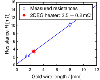
The NT heater resistance, which determines the magnitude of , could not be measured in situ, and was inferred from measurements of similar wires of different lengths shown in Fig. S2.
VII 2DEG resistance measurements
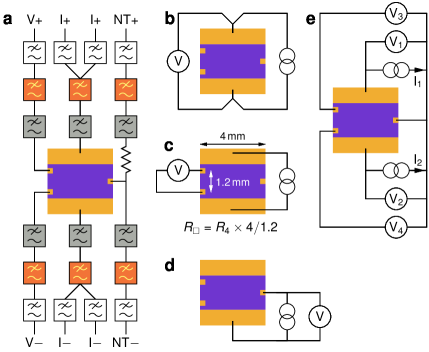

In addition to the filtering shown in Fig. 2, extra filters were connected to I and I lines in the metal cell to provide independent current and voltage lines, as shown in Fig. S3a. Therefore the four-terminal resistance measurements that involve I contacts, such as , include Ag epoxy and Cu powder filters and the interconnecting Cu and NbTi wires, contributing less than 0.1 . Figure S3e shows that a measurement of does not require shorting the I and V ohmics. Signatures of superconductivity in the I ohmic contact are shown in Fig. S4. Table S2 summarises all the relevant low temperature resistances.
A different sample of identical design, also fabricated using wafer W476, was investigated in the plastic cell. The LED was situated outside the cell and the light had to travel through the cell wall, leading to less efficient illumination, see Table S2, than in the metal cell. Single I connections increased the uncertainty in . The absence of NT lines made in-situ measurements involving the NT ohmic contact impossible.
Before After illumination illumination 32.5 6.4 16.8 4.4 31.0 7.7 31.4 7.7 26.8 6.1
Before After illumination illumination 48.0 15.3
VIII 3He temperature
The plastic immersion cell was equipped with a 3He noise thermometer, see Fig. S5. A 25 m Au wire was wedge-bonded between two sintered 1 mm Ag wires. The whole assembly was enclosed in a leak-tight Stycast 1266 appendix cell, connected to the main cell with a capillary and surrounded with a Nb shield. The temperature of this composite Au+Ag resistor was read out with a SQUID current sensor. It was found to be within 20 K of the nuclear stage temperature down to 0.5 mK, see Fig. S5.
A similar thermometer was not implemented in the metal cell, to avoid the construction overheads associated with bringing an additional twisted pair into the shielded environment. The low-heat leak nature of this environment plus significantly reduced amount of amorphous dielectrics in contact with 3He, in comparison with the plastic cell, allow us to conclude that the thermalisation of the 3He bath in this metal cell was at least as good as in the plastic cell. Therefore the temperature of the nuclear stage, monitored in the experiment with the metal cell, gives an accurate measure of the 3He bath temperature .
IX 2DEG Noise thermometer correction
The sintered silver heat sinks at , see Fig. 2, installed to reduce , contribute % of the 2DEG NT resistance , see Fig. S6. The measured Johnson voltage noise power
| (S1) |
gives the raw NT reading , allowing us to infer the temperature of the NT gold wire
| (S2) |
The sub-K gradient between the 3He bath temperature and the measured nuclear stage temperature down to 0.3 mK results in a negligible 1 K error in .
X Additional thermal transport and heat leak measurements
Figure S7 illustrates measurements of thermal conductances and heat leaks in the preliminary and auxiliary immersion cell runs. In contrast to the main experimental run, referred to below as M, in all of these measurements the immersion cells were filled with pure 3He, resulting in 2D solid 3He adsorbed on all surfaces inside the cells and consequently increased [48]. For each NT and NT heater the NT correction factor and heater resistance were obtained using procedures described above. The coefficients in thermal conductance models obtained in the fits are summarised in Table S3.
Before After illumination illumination 0.24 0.33 W/K W/K W/K W/K W/K4.2 W/K
Run A. A 4 mm4 mm 2DEG device was cooled in the plastic immersion cell with Cu powder filters. The sample was damaged during disassembly after the run, and so a second sample from wafer W476 and with similar electrical characteristics was used in the metal cell. Figure S7a shows the non-local thermal conductance measured between 7 and 30 mK, which was found to follow
| (S3) |
behaviour that is consistent with a sum of and terms (see Eqs. (2) and (S5)) observed in runs M and B. Unlike those runs, is independent of the illumination, which may reflect a more favourable layout of the gold wire bonds to the I ohmics in run A. The heat leak was inferred from measurements of vs at , Fig. S7d, and integrating Eq. (S3)
| (S4) |
Equation (S4) gave consistent results above mK. This was not the case at lower temperatures suggesting that does not extrapolate to low temperatures according to Eq. (S3). Therefore the data at mK, shown in grey in Fig. S7d, were excluded from the determination of . Due to the lack of NT heater and could not be measured directly, so in Fig. 1c was roughly estimated using the parameters derived for the second 2DEG device, with the heat leak being the only input from Run A.
Run B. The second 2DEG device was cooled in the metal cell with Cu powder filters. In this run was found to follow
| (S5) |
see Fig. S7a, with and obtained in run M, Eq. (2). This corresponds to the thermal conductance between the NT and the 3He bath
| (S6) |
with given by Eq. (1). Here represents an extra channel in due to the nuclear magnetism of 2D solid 3He absorbed on the noise thermometer assembly when the cell is filled with pure 3He in run B, but suppressed by 4He plating in run M [48]. The discrepancy between measured in run B and Eq. (S6) below 7 mK, see Fig. S7c, is attributed to the breakdown of the differential thermal conductance measurement in the presence of significant , in the regime where is temperature-dependent. The heat leak, Fig. S7e, was measured by the same procedure as in run A and the extrapolation of the measured was found to hold down to 2 mK.
Run C. To measure separately from , an NT + gold thermal link + NT heater assembly was installed in the plastic cell, similar to that used in the metal cell, but with no 2DEG and with the NT ohmic contact substituted with a gold bonding pad on a silicon chip. The total length of the NT + thermal link + heater gold wire chain was similar to the metal cell, with a surface area of 0.8 mm2. Figure S7c shows the Kapitza conductance between this gold wire and 3He that follows
| (S7) |
with the same as in Eq. (1), but without the term and with smaller than observed run B, Eq. (S5). We attribute this discrepancy to the strong thermal link between the 0.04 mm2 surface of the NT ohmic contact and 3He, potentially related to the coupling between 3He nuclear spins and magnetic Ni in the ohmic contact. The heat leak, Fig. S7f was obtained as
| (S8) |
Run C provides the upper bound on for runs A and B and justifies ignoring the small when evaluating much larger .
Run D. After the end of run M, the gold thermal link between NT ohmic and NT was replaced with aluminium. Isolating the NT from the 2DEG and NT heater, allowed us to measure just the heat leak into the 1.6 mm long NT, as opposed to run C, where the combined heat leak into 10 mm long chain of gold wires was measured. To obtain the heat leak, Fig. S7f, we scale in Eq. (S8) by the wire length. This provides the lower bound on for run M, and allows us to obtain an upper bound on and , which is the main purpose of our thermal model.
XI Potential improvements in cooling
Here we consider the cooling of the 2DEG device characterised in the metal cell in the absence of the superconductivity in the ohmics, while retaining all other parameters. We expect to obtain such conditions when a magnetic field of 0.1 T is applied parallel to the plane of the 2DEG [46]. With the I ohmics fully contributing to the cooling of the 2DEG, they dominate , Fig. 3g, therefore (two halves of connected in parallel). Using the resistances measured at 1.0 K, above , , before (after) illumination, as measured above . Then for mK and Eqs. (3) and (4) give . By optimising the fridge and heat exchanger performance we expect a bath temperature of mK and an electron temperature in the 2DEG of .
If the superconductivity is to be tolerated, an overlayer of evaporated gold or a network of gold wirebonds can improve the effectiveness of the large I contacts at least to the level of the small NT ohmic. By scaling the effective contact resistance of the latter with the perimeter we get for each I and I. As these ohmics now dominate the smaller V, we estimate . Assuming that the extra gold does not change the small NT ohmic significantly, we take to be unchanged by this procedure. This gives , before (after) illumination leading to at and mK in both cases.