An Integrated Widefield Probe for Practical Diamond Nitrogen-Vacancy Microscopy
Abstract
The widefield diamond nitrogen-vacancy (NV) microscope is a powerful instrument for imaging magnetic fields. However, a key limitation impeding its wider adoption is its complex operation, in part due to the difficulty of precisely interfacing the sensor and sample to achieve optimum spatial resolution. Here we demonstrate a solution to this interfacing problem that is both practical and reliably minimizes NV-sample standoff. We built a compact widefield NV microscope which incorporates an integrated widefield diamond probe with full position and angular control, and developed a systematic alignment procedure based on optical interference fringes. Using this platform, we imaged an ultrathin () magnetic film test sample, and conducted a detailed study of the spatial resolution. We reproducibly achieved an estimated NV-sample standoff (and hence spatial resolution) of at most across a field of view. Guided by these results, we suggest future improvements for approaching the optical diffraction limit. This work is a step towards realizing a widefield NV microscope suitable for routine high-throughput mapping of magnetic fields.
Magnetic imaging using nitrogen-vacancy (NV) centers in diamond[1] has proven to be a valuable technique for studying the magnetic and electronic properties of materials and devices[2, 3]. One particular approach, widefield NV microscopy, involves imaging an ensemble of NVs residing in a thin () layer within the diamond, whose spin states are read out via their optically detected magnetic resonance (ODMR) spectrum with a camera to map the stray magnetic field of a proximal sample[4, 5, 6]. This technique has found utility in imaging a wide array of devices[7, 8, 9, 10, 11, 12, 13, 14, 15], as well as biological[16, 17, 18, 19] and geological[20, 21, 22] samples. While greater spatial resolution is achievable using scanning NV microscopy[2, 3], the parallel operation and high magnetic sensitivity of the widefield modality makes it well-suited to rapid, multi-purpose diagnostic imaging of magnetic materials and devices[6]. However, its ease of use and potential for high-throughput imaging is often limited in practice by the requirement that the NV layer (and hence diamond sensor) be placed in close proximity with the sample. This is a challenge, as both the sensor and sample are relatively bulky objects (up to millimeters in size). Departures from flatness such as sample surface features or contaminants will cause misalignment between the diamond and sample surfaces resulting in standoffs which can significantly reduce image resolution. Broadly speaking, there are two ways to interface the diamond sensor with the sample[6]. In the first case, termed “sample-on-diamond”, the sample is fabricated directly onto the diamond surface. This method is ideal for minimizing standoff (to s of nanometers [9, 16, 11, 13]), however it is impractical for measurements of many samples or for samples which cannot be fabricated in-house. In the second case, termed “diamond-on-sample”, the diamond sensor is independent from the sample, either placed on the sample or held in contact. This second method partly solves the practicality problem, but makes standoff minimization more difficult, with standoff values as large as frequently reported[10, 22, 12, 14]. Here we present a widefield NV microscope with the flexibility of the “diamond-on-sample” method, while also demonstrating a systematic method for minimizing standoff.
Our approach follows the method demonstrated by Ernst et al. [23]. They reported the application of interferometry to scanning planar probe microscopy, showing that in situations involving a planar sensor parallel to a planar sample, the distance between probe and sample can be reliably minimized by first rotationally aligning the surfaces using interferometry as a feedback mechanism. They implemented this scheme for a sized sample and millimeter-sized sensor, achieving standoff at the point of contact, allowing for nanometer-scale imaging through scanning. Here, we extend this concept to larger surface contact areas, as required for widefield imaging of large (millimeter to centimeter) scale samples. In the case of widefield imaging, standoff of 100s of nanometers is often sufficient to achieve near-optimum spatial resolution, relaxing the technical requirements. Therefore, we implement a simplified and manual version of the alignment method which is suitable in this regime.
Our platform is based on a “widefield probe” which allows angular control of the diamond (the probe) with respect to the fixed sample [Fig. 1(a)]. The widefield probe is constructed on a miniature printed circuit board (PCB) integrating a microwave loop antenna around a through hole (for imaging), and attached to a holding arm [Fig. 1(b)]. The size of the loop and hole can be varied depending on the application; all measurements here used a hole diameter. A thick glass coverslip is glued over the through hole, and the diamond is adhered to the coverslip using low fluorescence glue. The arm is attached to a 5-axis stage: 2-axis rotation (rotation + goniometer) configured to allow angular adjustment of the diamond surface with minimal translation, and 3-axis linear motion for positioning and focusing. Finally, this probe stage is integrated into a compact () footprint but otherwise standard widefield NV microscope [Fig. 1(c)]. Long working distance ( cm) coverslip corrected objective lenses (10x and 20x ) are used to give sufficient clearance for the probe, as shown in Fig. 2(a).
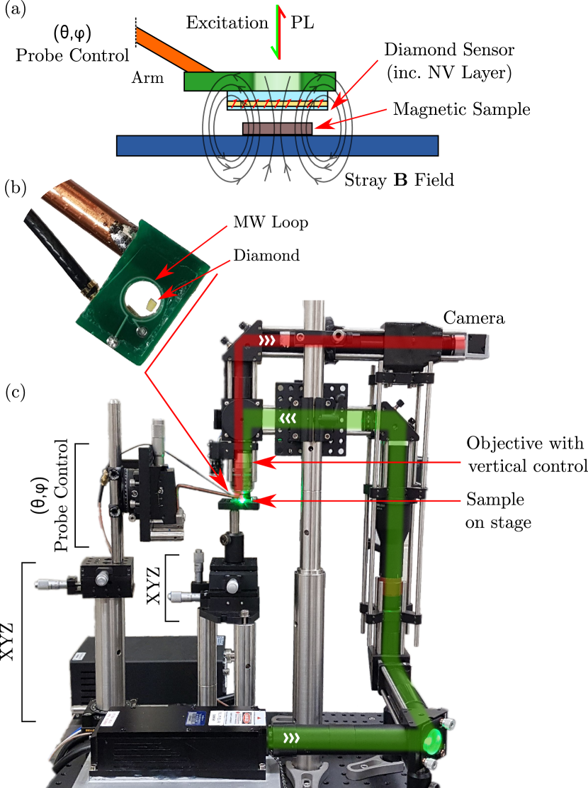
To test our method and evaluate integrated system performance, we imaged an ultrathin film, millimeter-sized magnetic device fabricated on a Si/SiO2 substrate [Fig. 2(b)]. The film is a W/CoFeB/MgO stack with a thick CoFeB layer exhibiting perpendicular magnetic anisotropy[24]. The diamond used was a thick, -oriented, high-pressure high-temperature (HPHT) diamond with a NV layer near the surface formed by ion implantation[25] [see further details in Supplementary Section I]. A section of the diamond was laser cut and attached to the widefield probe [Fig. 1(b)]. When focusing the objective onto the sample surface with the diamond at some distance, the device structure is visible in the reflected NV PL [Fig. 2(c)].
To align the probe with this device, we proceed as follows. As the diamond and sample are coarsely brought together, interference fringes due to angular displacement become faintly visible in the PL image [examples will be shown in Fig. 3]. The fringes are due to interference of the collimated excitation beam between diamond and sample surface, resulting in patterned NV excitation and hence modulated PL. Orientation alignment is performed while there is a small air gap between the diamond and sample. Adjusting the diamond angle causes the fringes to rotate and spread along the axis least aligned. Ideally, the fringes are ultimately spread such that only one band is visible. Finally, the diamond and sample are brought into direct contact by further vertical adjustment. The NV layer is first moved into focus, then the sample is brought up until it is seen to contact the diamond through the NV PL video feed (sample features come into focus, and the sample is stabilized when the diamond comes into contact). Compared with the method of Ernst et al. [23], this method is manual and does not allow estimation of the actual standoff directly.

After applying this alignment procedure, we proceed to acquire a magnetic image of the sample. To this end, the NV PL of a region of the diamond is imaged as the microwave frequency is swept, resulting in an ODMR spectrum for each pixel of the image. The sweep is repeated and images are integrated (per frequency bin) to improve the signal to noise ratio. The data is fit numerically to determine the position of the ODMR peaks and of a given NV orientation class, and hence calculate the projected magnetic field , where is the NV gyromagnetic ratio. An example magnetic image is shown in Fig. 2(d), which reveals device features such as the two large magnetic pads and the rungs connecting them. The relatively clean magnetic image contrasts with the comparatively dirty optical image [Fig. 2(c)], despite some residual imaging artifacts attributed to diamond features and off-axis bias field alignment [see Supplementary Section IV]. Note that in Fig. 2(d) the bias field of was removed via a three-point plane subtraction. The resulting image was obtained using a 10x objective, providing a field of view (FOV) of at pixels (pixel size ). Magnetic features such as the rungs were resolved after minutes of integration. To resolve micron-scale details required integration times on the order of hours. As seen in the zoom-in magnetic image and scanning electron microscope image [Fig. 2(e-f)], magnetic bars down to a width of can be resolved. All resolved features are separated by implying that the resolution is at or below .
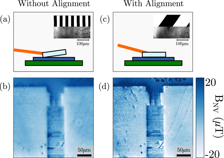
To illustrate the importance of the alignment step, we show images resulting from two different imaging conditions, obtained using a 20x objective (hence, resulting in a smaller FOV compared to Fig. 2(d)). In the first case, no angular alignment is performed [Fig. 3(a)], and fringes are visible in PL [Inset to (a) and Supplementary Fig. S2(a)]. As a result, the magnetic image is blurry [Fig. 3(b)]. We found that forcing the diamond into a closer contact without first performing alignment does not actually reduce the standoff, which can be understood by considering the schematic in Fig. 3(a), where the diamond contacts the sample at a point resulting in non-uniform standoff. We also “dropped” the diamond onto the sample and took ODMR images with microwaves provided by a PCB. This produced similarly blurry magnetic images. This is likely due to either sample surface features or contaminants causing similar point like contact, resulting in the diamond resting at an angle. In contrast, minimizing the angle through monitoring the fringes before lowering the diamond reliably produced the sharpest images [Fig. 3(c,d)]. This is because the aligned diamond will overall be within close proximity with the sample. Alignment is maintained while contact is made, thus the aforementioned contact points may be forced away (i.e. contaminants) or otherwise only limit overall standoff to a small distance, rather than causing large standoff. The relative tilt between sensor and sample plane is determined by the fringe separation. The full PL FOV for the 10x objective is (this is cropped by a factor for the magnetic image in Fig. 2(d)). Thus, once a single fringe is visible, the relative tilt between sensor and sample planes is within . This corresponds to variation in standoff across the FOV. We found this precision to be sufficient for noticeable improvement compared to not performing alignment.
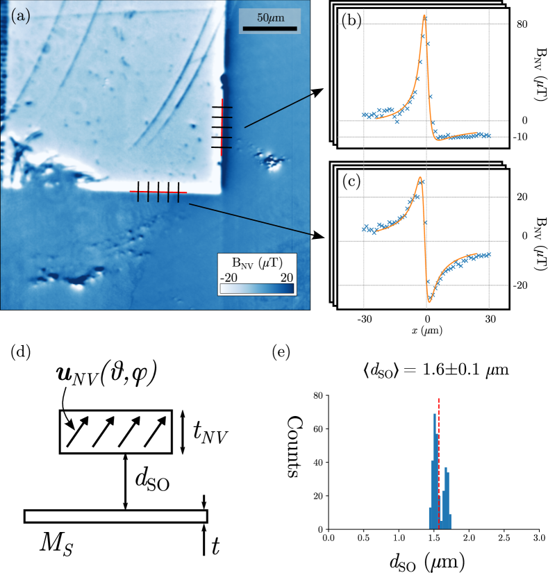
Having demonstrated a reliable way to align the NV-sample interface, we now investigate the factors affecting spatial resolution in the magnetic images. Firstly there are ‘optical’ effects such as diffraction, and also aberrations due to imaging through the diamond and coverslip. These effects limit the resolution in imaging the PL of the NV layer, independent of sample. Secondly, there are ‘standoff’ effects, namely the fact that the stray magnetic field seen by the NV layer is a convolution of the sample’s magnetization with a resolution function whose width is proportional to the NV-sample standoff [26, 3], as well as averaging over the finite thickness of the NV layer[27]. To estimate , we follow the method in Hingant et al. [28], analyzing line-cuts over the edge of the large magnetic pads [Fig. 4(a-c)]. The model is given by the theoretical stray field at a free standoff , integrated over the NV layer thickness, and convolved with a Gaussian function of fixed width to capture optical effects. The other free parameters are the NV orientation [spherical coordinates ] and sample spontaneous magnetization . The assumed parameters are the film thickness () and NV layer thickness, approximated to be with a uniform distribution [Fig. 4(d)]. Although in principle the optical resolution may be worse (larger profile width) than the diffraction limit, we approximate them to be equal, which resulted in a good model fit. This leads to the estimated standoff being an upper bound for the actual standoff. The analysis of Fig. 4(a), which was obtained using the 20x objective, leads to [Fig. 4(e)]. Similarly, from the image in Fig. 2(d) which used the 10x objective, we find . Such physical standoffs are similar to the best values reported by dropping the diamond and manual trial and error[29, 8], and significantly improved compared to more typical values on the order of [10, 22, 12, 14]. Together, the standoff and optical resolution combine to give an effective spatial resolution for a magnetic edge of [See Supplementary Section VI]. This value is dominated by the effect of standoff, as the stray field over an edge has a width of [30]. Including NV layer thickness, the contribution due to standoff is roughly that of diffraction, hence improvements to the effective resolution should first involve further minimization of , followed by improvements to and finally the diffraction limit. Note that for a magnetic dipole, the stray field width is approximately equal to [See Supplementary Section V], giving a resolution of in our case when trying to resolve dipole-like magnetic objects. From the model fit, we also obtain and , finding they are broadly consistent with expectations [See Supplementary Section V].
Overcoming standoff limitations will require finer angular and vertical control of the probe, easily accomplished using robotic stages[23]. Keeping the surfaces clean and flat to further reduce should be readily achievable. Neglecting NV layer thickness, to attain an effective resolution roughly the diffraction limit for a objective requires the standoff to be . To ensure the NV layer thickness is not limiting, diamonds with a thinner ( nm) layer should be used, at the expense of a reduced magnetic sensitivity[25]. Secondly, diffraction-limited optical resolution should be attainable by using a thinner diamond or customized optical components to minimize aberrations. A final resolution improvement can be achieved by lowering the diffraction limit, down to nm using an objective with . This will require some optimization of the widefield probe design to accommodate the millimeter-scale working distance of such high-NA objectives.
In summary, we demonstrated an NV microscope based on an integrated widefield NV probe which provides a rapid and reliable way to interface the probe with the sample, making our system ideal for high-throughput measurements of a range of magnetic samples and electronic devices. From our analysis of spatial resolution, we found the effective spatial resolution to be dominated by standoff. With further optimization of the spatial resolution and automation of the alignment procedure, there is an excellent prospect for this instrument to become a routine magnetic imaging technique.
Acknowledgements.
We thank V. Jacques for providing the CoFeB sample, which was originally grown and patterned by M. Hayashi, K. Garcia and J.-P. Adam. This work was supported by the Australian Research Council (ARC) through grants CE170100012, DP190101506 and FT200100073. We acknowledge the AFAiiR node of the NCRIS Heavy Ion Capability for access to ion-implantation facilities. S.C.S gratefully acknowledges the support of an Ernst and Grace Matthaei scholarship. A.J.H. is supported by an Australian Government Research Training Program Scholarship.Data Availability Statement
The data that support the findings of this study are available from the corresponding author upon reasonable request.
Author Declarations
The authors have no conflicts to disclose.
References
References
- Doherty et al. [2013] M. W. Doherty, N. B. Manson, P. Delaney, F. Jelezko, J. Wrachtrup, and L. C. L. Hollenberg, “The nitrogen-vacancy colour centre in diamond,” Phys. Rep. 528, 1–45 (2013).
- Rondin et al. [2014] L. Rondin, J.-P. Tetienne, T. Hingant, J.-F. Roch, P. Maletinsky, and V. Jacques, “Magnetometry with nitrogen-vacancy defects in diamond,” Rep. Prog. Phys. 77, 056503 (2014).
- Casola, van der Sar, and Yacoby [2018] F. Casola, T. van der Sar, and A. Yacoby, “Probing condensed matter physics with magnetometry based on nitrogen-vacancy centres in diamond,” Nat. Rev. Mater. 3, 17088 (2018).
- Steinert et al. [2010] S. Steinert, F. Dolde, P. Neumann, A. Aird, B. Naydenov, G. Balasubramanian, F. Jelezko, and J. Wrachtrup, “High sensitivity magnetic imaging using an array of spins in diamond,” Rev. Sci. Instrum. 81, 043705 (2010).
- Levine et al. [2019] E. V. Levine, M. J. Turner, P. Kehayias, C. A. Hart, N. Langellier, R. Trubko, D. R. Glenn, R. R. Fu, and R. L. Walsworth, “Principles and techniques of the quantum diamond microscope,” Nanophotonics 8, 1945–1973 (2019).
- Scholten et al. [2021] S. C. Scholten, A. J. Healey, I. O. Robertson, G. J. Abrahams, D. A. Broadway, and J. P. Tetienne, “Widefield quantum microscopy with nitrogen-vacancy centers in diamond: strengths, limitations, and prospects,” (2021), arXiv:2108.06060 [physics.app-ph] .
- Nowodzinski et al. [2015] A. Nowodzinski, M. Chipaux, L. Toraille, V. Jacques, J. F. Roch, and T. Debuisschert, “Nitrogen-Vacancy centers in diamond for current imaging at the redistributive layer level of Integrated Circuits,” Microelectronics Reliability 55, 1549–1553 (2015).
- Simpson et al. [2016] D. A. Simpson, J.-P. Tetienne, J. M. McCoey, K. Ganesan, L. T. Hall, S. Petrou, R. E. Scholten, and L. C. L. Hollenberg, “Magneto-optical imaging of thin magnetic films using spins in diamond,” Sci. Rep. 6, 22797 (2016).
- Tetienne et al. [2017] J.-P. Tetienne, N. Dontschuk, D. A. Broadway, A. Stacey, D. A. Simpson, and L. C. L. Hollenberg, “Quantum imaging of current flow in graphene,” Sci. Adv. 3, e1602429 (2017).
- Toraille et al. [2018] L. Toraille, K. Aïzel, É. Balloul, C. Vicario, C. Monzel, M. Coppey, E. Secret, J.-M. Siaugue, J. Sampaio, S. Rohart, N. Vernier, L. Bonnemay, T. Debuisschert, L. Rondin, J.-F. Roch, and M. Dahan, “Optical Magnetometry of Single Biocompatible Micromagnets for Quantitative Magnetogenetic and Magnetomechanical Assays,” Nano Lett. 18, 7635–7641 (2018).
- Broadway et al. [2020a] D. A. Broadway, S. C. Scholten, C. Tan, N. Dontschuk, S. E. Lillie, B. C. Johnson, G. Zheng, Z. Wang, A. R. Oganov, S. Tian, C. Li, H. Lei, L. Wang, L. C. L. Hollenberg, and J.-P. Tetienne, “Imaging Domain Reversal in an Ultrathin Van der Waals Ferromagnet,” Adv. Mater. 32, 2003314 (2020a).
- Turner et al. [2020] M. J. Turner, N. Langellier, R. Bainbridge, D. Walters, S. Meesala, T. M. Babinec, P. Kehayias, A. Yacoby, E. Hu, M. Lončar, R. L. Walsworth, and E. V. Levine, “Magnetic Field Fingerprinting of Integrated-Circuit Activity with a Quantum Diamond Microscope,” Phys. Rev. Applied 14, 014097 (2020).
- Ku et al. [2020] M. J. H. Ku, T. X. Zhou, Q. Li, Y. J. Shin, J. K. Shi, C. Burch, L. E. Anderson, A. T. Pierce, Y. Xie, A. Hamo, U. Vool, H. Zhang, F. Casola, T. Taniguchi, K. Watanabe, M. M. Fogler, P. Kim, A. Yacoby, and R. L. Walsworth, “Imaging viscous flow of the Dirac fluid in graphene,” Nature 583, 537–541 (2020).
- Meirzada et al. [2021] I. Meirzada, N. Sukenik, G. Haim, S. Yochelis, L. T. Baczewski, Y. Paltiel, and N. Bar-Gill, “Long-Time-Scale Magnetization Ordering Induced by an Adsorbed Chiral Monolayer on Ferromagnets,” ACS Nano 15, 5574–5579 (2021).
- Nava Antonio et al. [2021] G. Nava Antonio, I. Bertelli, B. G. Simon, R. Medapalli, D. Afanasiev, and T. van der Sar, “Magnetic imaging and statistical analysis of the metamagnetic phase transition of FeRh with electron spins in diamond,” J. Appl. Phys. 129, 223904 (2021).
- Le Sage et al. [2013] D. Le Sage, K. Arai, D. R. Glenn, S. J. DeVience, L. M. Pham, L. Rahn-Lee, M. D. Lukin, A. Yacoby, A. Komeili, and R. L. Walsworth, “Optical magnetic imaging of living cells,” Nature 496, 486–489 (2013).
- Glenn et al. [2015] D. R. Glenn, K. Lee, H. Park, R. Weissleder, A. Yacoby, M. D. Lukin, H. Lee, R. L. Walsworth, and C. B. Connolly, “Single-cell magnetic imaging using a quantum diamond microscope,” Nat. Methods 12, 736–738 (2015).
- Fescenko et al. [2019] I. Fescenko, A. Laraoui, J. Smits, N. Mosavian, P. Kehayias, J. Seto, L. Bougas, A. Jarmola, and V. M. Acosta, “Diamond Magnetic Microscopy of Malarial Hemozoin Nanocrystals,” Phys. Rev. Applied 11, 034029 (2019).
- McCoey et al. [2020] J. M. McCoey, M. Matsuoka, R. W. Gille, L. T. Hall, J. A. Shaw, J.-P. Tetienne, D. Kisailus, L. C. L. Hollenberg, and D. A. Simpson, “Quantum Magnetic Imaging of Iron Biomineralization in Teeth of the Chiton Acanthopleura hirtosa,” Small Methods 4, 1900754 (2020).
- Fu et al. [2014] R. R. Fu, B. P. Weiss, E. A. Lima, R. J. Harrison, X.-N. Bai, S. J. Desch, D. S. Ebel, C. Suavet, H. Wang, D. Glenn, D. L. Sage, T. Kasama, R. L. Walsworth, and A. T. Kuan, “Solar nebula magnetic fields recorded in the Semarkona meteorite,” Science 346, 1089–1092 (2014).
- Glenn et al. [2017] D. R. Glenn, R. R. Fu, P. Kehayias, D. L. Sage, E. A. Lima, B. P. Weiss, and R. L. Walsworth, “Micrometer-scale magnetic imaging of geological samples using a quantum diamond microscope,” Geochem. Geophys. Geosystems 18, 3254–3267 (2017).
- Fu et al. [2020] R. R. Fu, E. A. Lima, M. W. R. Volk, and R. Trubko, “High-Sensitivity Moment Magnetometry With the Quantum Diamond Microscope,” Geochem. Geophys. Geosystems 21, e2020GC009147 (2020).
- Ernst et al. [2019] S. Ernst, D. M. Irber, A. M. Waeber, G. Braunbeck, and F. Reinhard, “A Planar Scanning Probe Microscope,” ACS Photonics 6, 327–331 (2019).
- Gross et al. [2016] I. Gross, L. J. Martínez, J.-P. Tetienne, T. Hingant, J.-F. Roch, K. Garcia, R. Soucaille, J. P. Adam, J.-V. Kim, S. Rohart, A. Thiaville, J. Torrejon, M. Hayashi, and V. Jacques, “Direct measurement of interfacial dzyaloshinskii-moriya interaction in heterostructures with a scanning NV magnetometer ,” Phys. Rev. B 94, 064413 (2016).
- Healey et al. [2020] A. J. Healey, A. Stacey, B. C. Johnson, D. A. Broadway, T. Teraji, D. A. Simpson, J.-P. Tetienne, and L. C. L. Hollenberg, “Comparison of different methods of nitrogen-vacancy layer formation in diamond for wide-field quantum microscopy,” Phys. Rev. Materials 4, 104605 (2020).
- Lima and Weiss [2009] E. A. Lima and B. P. Weiss, “Obtaining vector magnetic field maps from single-component measurements of geological samples,” J. Geophys. Res. Solid Earth 114, B06102 (2009).
- Broadway et al. [2020b] D. Broadway, S. Lillie, S. Scholten, D. Rohner, N. Dontschuk, P. Maletinsky, J.-P. Tetienne, and L. Hollenberg, “Improved Current Density and Magnetization Reconstruction Through Vector Magnetic Field Measurements,” Phys. Rev. Applied 14, 024076 (2020b).
- Hingant et al. [2015] T. Hingant, J.-P. Tetienne, L. J. Martínez, K. Garcia, D. Ravelosona, J.-F. Roch, and V. Jacques, “Measuring the magnetic moment density in patterned ultrathin ferromagnets with submicrometer resolution,” Phys. Rev. Applied 4, 014003 (2015).
- Bertelli et al. [2020] I. Bertelli, J. J. Carmiggelt, T. Yu, B. G. Simon, C. C. Pothoven, G. E. W. Bauer, Y. M. Blanter, J. Aarts, and T. van der Sar, “Magnetic resonance imaging of spin-wave transport and interference in a magnetic insulator,” Sci. Adv. 6, eabd3556 (2020).
- Tetienne et al. [2015] J.-P. Tetienne, T. Hingant, L. J. Martínez, S. Rohart, A. Thiaville, L. H. Diez, K. Garcia, J.-P. Adam, J.-V. Kim, J.-F. Roch, I. M. Miron, G. Gaudin, L. Vila, B. Ocker, D. Ravelosona, and V. Jacques, “The nature of domain walls in ultrathin ferromagnets revealed by scanning nanomagnetometry,” Nature Communications 6, 6733 (2015).
- Capelli et al. [2019] M. Capelli, A. Heffernan, T. Ohshima, H. Abe, J. Jeske, A. Hope, A. Greentree, P. Reineck, and B. Gibson, “Increased nitrogen-vacancy centre creation yield in diamond through electron beam irradiation at high temperature,” Carbon 143, 714–719 (2019).
- Manson et al. [2018] N. B. Manson, M. Hedges, M. S. J. Barson, R. Ahlefeldt, M. W. Doherty, H. Abe, T. Ohshima, and M. J. Sellars, “NV- – N+ pair centre in 1b diamond,” New J. Phys. 20, 113037 (2018).
- Broadway et al. [2018] D. A. Broadway, N. Dontschuk, A. Tsai, S. E. Lillie, C. T.-K. Lew, J. C. McCallum, B. C. Johnson, M. W. Doherty, A. Stacey, L. C. L. Hollenberg, and J.-P. Tetienne, “Spatial mapping of band bending in semiconductor devices using in situ quantum sensors,” Nat. Electron. 1, 502–507 (2018).
- Thiel et al. [2019] L. Thiel, Z. Wang, M. A. Tschudin, D. Rohner, I. Gutiérrez-Lezama, N. Ubrig, M. Gibertini, E. Giannini, A. F. Morpurgo, and P. Maletinsky, “Probing magnetism in 2D materials at the nanoscale with single-spin microscopy,” Science 364, 973–976 (2019).
- Virtanen et al. [2020] P. Virtanen, R. Gommers, T. E. Oliphant, M. Haberland, T. Reddy, D. Cournapeau, E. Burovski, P. Peterson, W. Weckesser, J. Bright, S. J. van der Walt, M. Brett, J. Wilson, K. J. Millman, N. Mayorov, A. R. J. Nelson, E. Jones, R. Kern, E. Larson, C. J. Carey, İ. Polat, Y. Feng, E. W. Moore, J. VanderPlas, D. Laxalde, J. Perktold, R. Cimrman, I. Henriksen, E. A. Quintero, C. R. Harris, A. M. Archibald, A. H. Ribeiro, F. Pedregosa, P. van Mulbregt, and SciPy 1.0 Contributors, “SciPy 1.0: Fundamental Algorithms for Scientific Computing in Python,” Nature Methods 17, 261–272 (2020).
- Olivero and Longbothum [1977] J. Olivero and R. Longbothum, “Empirical fits to the Voigt line width: A brief review,” Journal of Quantitative Spectroscopy and Radiative Transfer 17, 233–236 (1977).
Supplementary Information
I NV-diamond sensor
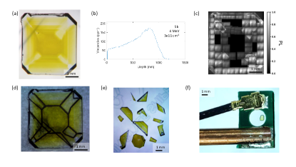
The NV-diamond samples used in this work were made from a type-Ib, single-crystal diamond substrate grown by high-pressure, high-temperature (HPHT) synthesis, with -oriented polished faces, purchased from Chenguang Machinery & Electric Equipment. The diamond featured multiple sectors with various levels of nitrogen content as inferred from the different shades of yellow [Fig. S1(a)], but all sectors had very low level of NV PL initially.
To form a dense NV layer near the surface, we implanted the diamond with MeV Sb ions with a dose of ions/cm2. We performed full cascade Stopping and Range of Ions in Matter (SRIM) Monte Carlo simulations to estimate the depth distribution of the created vacancies [Fig. S1(b)], predicting a distribution spanning the range - nm (approximated to a m layer in the main text) with a peak vacancy density of ppm at a depth of nm (assuming no dynamic annealing effects). Following implantation, the diamond was annealed at ∘C for 4 hours in a vacuum of Torr to form the NV centers. After annealing, the plate was acid cleaned ( minutes in a boiling mixture of sulphuric acid and sodium nitrate).
We then took a photoluminescence (PL) map [Fig. S1(c)] to identify the brightest sectors, as these gave the best magnetic sensitivity. These brightest sectors generally corresponded to the sectors with the lightest shade of yellow, indicating that the darker sectors have a high level of nitrogen such that electron tunnelling significantly quenches the PL[31, 32]. We then used a laser cutting system to isolate the best sectors [Fig. S1(d)], resulting in diamonds of lateral size each [Fig. S1(e)]. The diamond pieces were acid cleaned (same process as above) after laser cutting, leaving them ready for mounting on the widefield probe as described in the main text. A photo of such a probe as seen from above (objective side) is shown in Fig. S1(f).
II Experimental setup
The experimental setup is shown in Fig. 1(c) of the main text. Continuous-wave (CW) laser excitation was produced by a nm solid-state laser outputting 1.5 W of power (Dragon Lasers FN series). The beam was attenuated to 300 mW, beam expanded (10x) and focused using a widefield lens () to the back aperture of the objective lens. We used two different objectives in this work: (i) Nikon S Plan Fluor 20x ELWD, NA = 0.45, working distance 6.9-8.2 mm; (ii) Nikon Plan Fluor 10x, NA = 0.3, working distance 16 mm. The PL from the NV layer was collected by the same objective, separated from the excitation light with a dichroic mirror, filtered using a longpass filter, and imaged using a tube lens ( mm) onto a CMOS camera (Basler acA2040-90um USB3 Mono).
Microwave excitation was provided by a signal generator (Windfreak SynthNV Pro) gated using a switch (Mini-Circuits ZASWA-2-50DR+) and amplified (Mini-Circuits ZHL-16W-43+). The output of the amplifier is directly connected to the PCB of the widefield probe using a coaxial cable. A pulse pattern generator (SpinCore PulseBlasterESR-PRO 400 MHz) was used to gate the microwave and to synchronise the image acquisition.
The optically detected magnetic resonance (ODMR) spectra of the NV layer were obtained by sweeping the microwave frequency, taking a reference image (microwave off) for each frequency in order to produce a normalized spectrum removing common-mode PL fluctuations. The exposure time for each camera frame was 20 ms (i.e. 40 ms per frequency), and the entire sweep was repeated thousands of times to improve the signal to noise ratio. A bias magnetic field of a few milliteslas was applied using a permanent magnet, roughly aligned (but not exactly) with one of the four possible NV orientation classes (corresponding to the crystal directions). We swept the microwave frequency in order to interrogate this mostly aligned NV family only. All measurements were performed in an ambient environment at room temperature.
III Alignment using PL
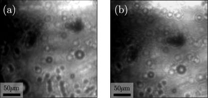
As mentioned in the main text, alignment is performed using optical fringes. The full PL images corresponding to the two different alignment conditions in main text Fig. 3 are shown in Fig. S2. The insets in main text Figs. 3(a,c) are sub-regions of these full PL images (with a rotation) selected to better highlight the fringes, with black/white stripes to guide the eye. While the interference fringes are quite difficult to see in these static images, they are relatively easy to identify in the live video feed as the angle is adjusted, enabling optimization.
The fringe spacing corresponds to the relative angle between the sensor and sample surfaces: where is the angular displacement, is the excitation wavelength () and is the fringe spacing.
IV Magnetic field imaging
The ODMR peaks are generally dependent on temperature, strain and magnetic field[1]. In the regime where the applied field along the NV axis is large compared to that perpendicular, are mostly dependent on magnetic field[2],
| (S1) |
where is the zero field splitting, is the gyromagnetic ratio and is the magnetic field projection along the NV axis.
In this aligned field regime, the magnetic field can then be deduced from the two ODMR frequencies,
| (S2) |
The maps in the main text were obtained in this way. Additionally, the zero-field splitting can be obtained via
| (S3) |
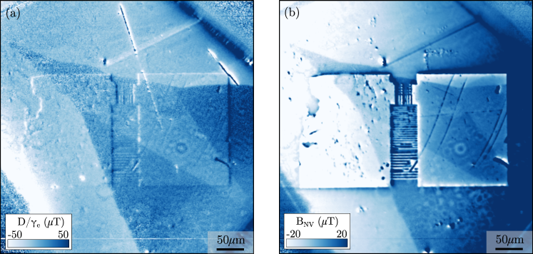
The map corresponding to the data in main text Fig. 2(d) is shown in Fig. S3. Large uniform sectors with different values are visible, which match sectors with different levels of nitrogen content in our HPHT diamond. The variation in between different sectors is attributed to differences in strain.
Comparing Fig. S3(b) (which is the same as Fig. 2(d) of the main text but without 3-point plane subtraction, and nominally representing ) with Fig. S3(a) (nominally representing ), we notice some correlations: the strain sectors are visible in the map, whereas the magnetic devices are visible in the map. This cross-talk is due to the fact that here the bias magnetic field was not well aligned with the NV axis. In the misaligned regime, Eq. S2 and S3 are only approximate relations[2], leading to an apparent cross-talk between the resulting maps. However, more accurate alignment or performing 8-peak ODMR (measuring all 4 NV orientation classes[33]) can reliably resolve this. For example, the magnetic images shown in Figs. 3 and 4 of the main text were obtained with a better bias field alignment, leading to significantly reduced strain-induced artifacts.
V Magnetic field fitting
The magnetic field along a line-cut perpendicular to an infinite edge of a perpendicularly magnetized film (spontaneous magnetization , thickness ) at standoff distance is given by[28]:
| (S4) | ||||
| (S5) |
where is along the line-cut (film edge at ) and is normal to the magnet plane. The magnetic field projection along the NV axis is then
| (S6) |
where are the spherical angles characterizing the NV axis direction.
Taking Eq. S4 to the thin film limit () gives a Lorentzian profile, with a full width at half maximum (FWHM) equal to [28]. This profile is the result of upwards continuation of the magnetic field from the sample plane (a delta function in this case for the component) to the sensing (NV) plane[26]. Thus, one can view the Lorentzian of width as the point spread function (PSF) associated with the stray field measurement at a finite standoff, which is a helpful concept when discussing spatial resolution. In general, however, the PSF may differ depending on the type of magnetic field source and the field component considered[3]. For example, in the case of a magnetic dipole oriented in the -direction, the profile of the component is narrower, having a FWHM approximately equal to . Nevertheless, the case of a film edge is of relevance for many applications for instance to 2D magnetic materials[34, 11]. Therefore, in the following discussion we take the effective spatial resolution (considering standoff effects only) to be .
To account for optical effects, Eq. S6 in principle needs to be convolved with the optical PSF, assumed to be a Gaussian profile with FWHM . As mentioned in the main text, we simply took where corresponds to the diffraction limit, which potentially results in an overestimate of . In future we plan to characterize more precisely. To account for a finite NV layer thickness , in Eq. S6 is replaced with , and the average is taken over . Thus:
| (S7) |
We assume the magnet to have uniform magnetization and thickness (). We also assume the standoff to be uniform across the image after alignment, hence is uniform. Actually, at alignment, no fringes are visible, hence fringe separation may be taken to be the full image width. This implies the maximum standoff variation between one edge and another is wavelength, i.e. . Thus the assumption that standoff is uniform amounts to estimating the average standoff across the image, whereas it would also be possible to map the variable standoff along the edges of the device. Simultaneously fitting pairs of orthogonal line-cuts extracted from two perpendicular edges (edge 1 and edge 2) [Fig. 4(a)], we can recover the magnetization , the NV angles and , and the standoff . Fitting is performed using non-linear least squares (using SciPy[35]), with the residual function of each pair given by:
| (S8) |
where and are the coordinate and data point of the line-cut respectively (). The parameters and are to center the fits to the data horizontally and vertically respectively. A histogram is constructed for each fit parameter, from which we calculate the measured value (mean) and an error estimate ( one standard deviation), which are the numbers discussed in the main text and given in Table S1. We measured (10x objective) and (20x), consistent with the expectation for a -oriented diamond (nominally ). We also measured (10x) and (20x), consistent with the previous measurement of the same sample with scanning NV magnetometry[24], . Not addressed in this work is the effect of delocalized contributions to the ODMR spectrum of each pixel due to reflections of PL internal to the diamond. In their experiment, Fu et al. estimated this background signal to contribute of measured spectra[22]. Applying the same factor here would result in a doubling of the value of measured. However, systematically determining the ratio of delocalized to local signal was beyond the scope of this experiment, and will be addressed in future work.
| Objective | ||||
|---|---|---|---|---|
| () | () | () | () | |
| 10x | ||||
| 20x |
is the standoff found when the NV layer thickness is neglected.
VI Optical and Magnetic Resolution
As discussed, resolution can be characterized by three operations: convolution with a Gaussian due to optical effects, convolution with a Lorentzian due to standoff, and averaging over the NV layer thickness. Note that the Gaussian is an approximation to the diffraction PSF which is an Airy disk, but we used a Gaussian as a more generic optical PSF, allowing us to test the scenario of a PSF broadened by aberrations, . However, we found the assumption to give the best fit to the data. To determine the effective resolution mentioned in the main text, we find the FWHM of an apparent PSF. This apparent PSF is given by the convolution of the Gaussian and Lorentzian PSFs, neglecting the averaging over the NV layer for simplicity. The resulting function is the Voigt profile. To account for the NV layer thickness, the Lorentzian PSF FWHM is replaced with FWHM , where is the apparent standoff determined by fitting the line-cuts to the data without including the averaging of the NV layer [See Table S1]. As expected, we find . The FWHM of a Voigt profile composed of a Gaussian of FWHM and Lorentzian of FWHM is well approximated by[36]:
| (S9) |
Thus the effective resolution is given by:
| (S10) |
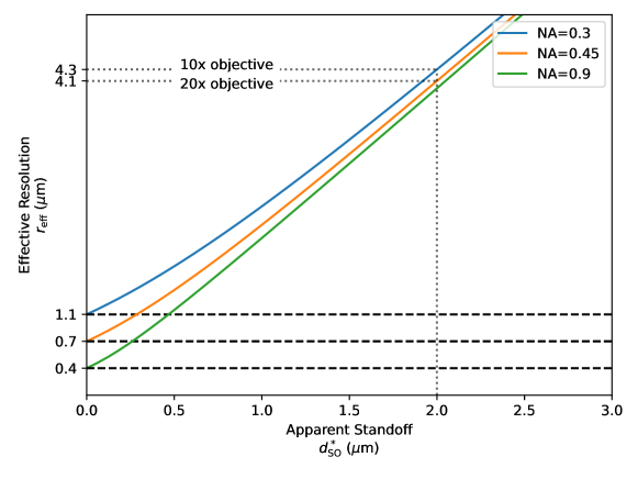
To illustrate the next steps in improving resolution, we graphed the NV-sample standoff against effective resolution for objectives with different numerical apertures [Fig. S4]. The measurements made in this work using the 10x and 20x objectives are shown. At zero standoff, the effective resolution is equal to the diffraction limited resolution.
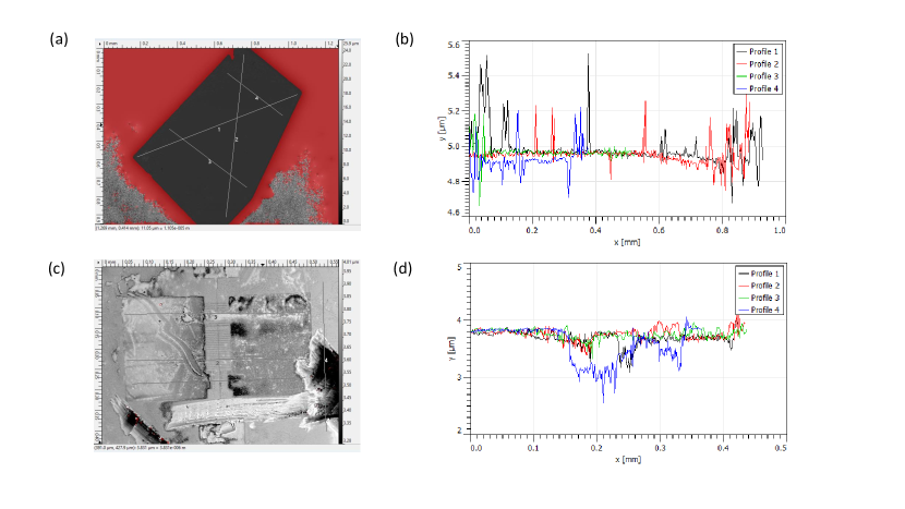
VII Optical Profilometry
As discussed in the main text, an obvious requirement for standoff minimization is that the sample and diamond surfaces are flat and free of protrusions. We characterized both the diamond and sample using optical profilometry. Note that (without further analysis) profilometry assumes the same material across the image, whereas for the sample there are different materials present, such as the large damaged region where the silicon substrate is exposed. Nevertheless, the protrusions from both surfaces appear to be sufficiently small compared with the standoff distances measured, indicating polishing and cleanliness were not limiting in our case. This detail will require further attention in order to reach the diffraction limit, which requires standoff.