Integrated Kerr frequency comb-driven silicon photonic transmitter
Abstract
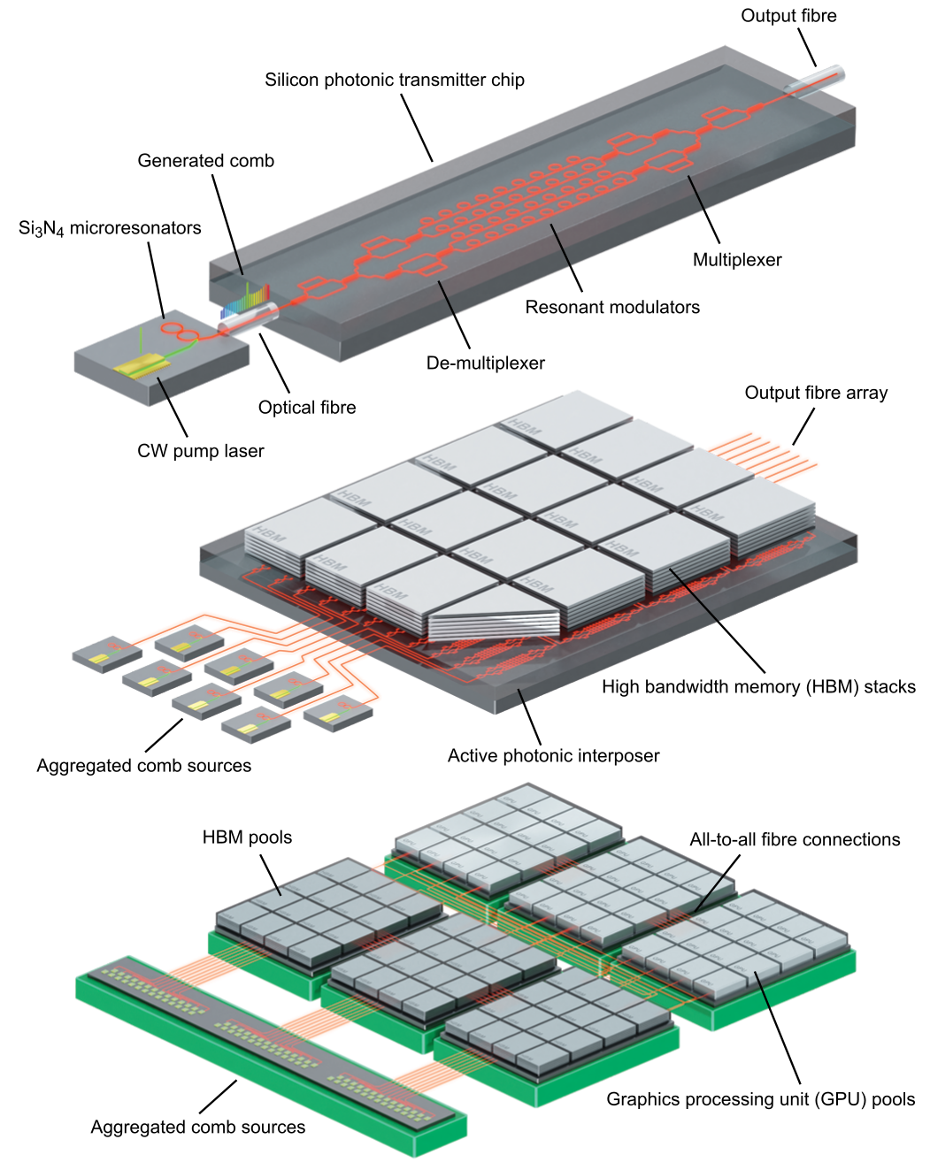
The exponential growth of computing needs for artificial intelligence and machine learning has had a dramatic impact on data centre energy consumption, which has risen to environmentally significant levels. Using light to send information between compute nodes can dramatically decrease this energy consumption while simultaneously increasing bandwidth. Through wavelength-division multiplexing with chip-based microresonator Kerr frequency combs, independent information channels can be encoded onto many distinct colours of light in the same optical fibre for massively parallel data transmission with low energy. While previous demonstrations have relied on benchtop equipment for filtering and modulating Kerr comb wavelength channels, data centre interconnects require a compact on-chip form factor for these operations. Here, we demonstrate the first integrated silicon photonic transmitter using a Kerr comb source. The demonstrated architecture is scalable to hundreds of wavelength channels, enabling a fundamentally new class of massively parallel terabit-scale optical interconnects for future green hyperscale data centres.
With the rise of cloud-based computing, computational workloads have largely been offloaded from local machines onto the server racks of hyperscale data centres and high-performance computers. Bandwidth-hungry applications such as artificial intelligence and machine learning have severely strained the interconnects within these systems, creating a threat of scaling stagnation without significant changes to the physical hardware used to pass data between nodes Cheng:18 ; Miller2000 . Furthermore, the energy consumption of such data centres has become environmentally significant strubell2019energy and will be dominated by interconnect energy in the aforementioned communication-intensive workloads. Optical interconnects based on silicon photonics have been widely recognized as a promising avenue for interconnects to keep pace with these ever-growing bandwidth demands while additionally decreasing energy consumption compared to their electrical counterparts. This promise is largely due to the compact footprint of silicon-on-insulator (SOI) devices, the compatibility of SOI photonics processes with the ubiquitous complementary metal-oxide-semiconductor (CMOS) infrastructure used to fabricate electronic chips, and the tremendous inherent parallelism provided by optics through dense wavelength division multiplexing (DWDM) Miller2009 ; miller_attojoule ; Sun2015 ; Atabaki2018 . In particular, DWDM enables independent information channels to be encoded on different colours of light simultaneously in a single optical waveguide or fibre, in stark contrast to copper wire-based links which only permit a single channel per physical connection.
The use of frequency combs for DWDM optical interconnects is an appealing prospect due to their ability to replace the currently-used large arrays of lasers with a single multi-wavelength source Hu2021 ; Gaeta2019 . For massively parallel wavelength scaling, microresonator-based Kerr frequency combs in the silicon nitride (Si3N4) platform show particular promise due to their compact size, CMOS compatibility, and ability to generate hundreds of evenly-spaced low-noise wavelength channels from a single continuous-wave (CW) laser source Levy2010 ; Levy2012 ; Kippenberg18 . Chip-based frequency combs have been widely demonstrated for long-reach optical communications using benchtop telecommunications equipment for filtering, modulating, and receiving wavelength channels Marin-Palomo2017 ; Pfeifle2014 ; Fulop2018 ; Kong:20 ; Hu2018 ; Corcoran2020 . However, DWDM has drawn a great deal of interest for data centre interconnects Ayar2020 ; Liang:20 ; Chen:15 , which place stringent requirements on the energy consumption and footprint of transceivers.
Notable demonstrations with semiconductor mode-locked lasers Chen:15 ; soa2017 and distributed feedback laser (DFB) arrays Zheng:13 have shown high bandwidth data communication with compact silicon photonic transmitter chips, but used modest wavelength channel counts (five, eight, and eight, respectively) and lack the inherent scalability provided by Kerr combs. In particular, semiconductor mode-locked lasers are fundamentally restricted in wavelength scaling by the gain bandwidth of the active region material Liu:19 , while DFB arrays suffer from non-uniform channel spacing due to fabrication variations between the discrete laser cavities as well as the need to multiplex all of the channels onto a single output fibre. A monolithic lithium niobate chip was used to demonstrate Kerr comb generation, filtering, and modulation on a single die, but was restricted to a single filtered channel at megabit/s data rates due to the noisy modulational instability state of the comb Wang2019 .
Here, we demonstrate the first integrated Kerr comb-driven silicon photonic transmitter using a novel, massively scalable link architecture. The transmitter was designed for 32 wavelength channels and showed open eye diagrams for all channels up to 16 Gb/s, yielding an aggregate single-fibre bandwidth of 512 Gb/s. Furthermore, the generated comb lines showed a negligible power penalty compared to a tunable CW laser source at the same wavelength, demonstrating that each tone behaves identically to an independent CW carrier from an array of lasers. This work represents a novel and realistic direction for data centre interconnects to scale to hundreds of wavelength channels, enabling future multi-terabit/s chip-to-chip links operating at energies below one picojoule per bit.
Results
While past demonstrations have focused on coherent communications using Kerr microcombs as DWDM sources, high performance computer and data centre interconnects require low latency and low energy per bit, making intensity-modulated direct-detection (IM-DD) solutions more appealing than coherent solutions due to the absence of energy-intensive and latency-inducing digital signal processing (DSP). In particular, IM-DD links with native error-free signaling do not require forward error correction (FEC) and thus have no encoding overhead, easing requirements on the electronics to reconstruct the original bit stream. Additionally, coherent communication links require a local oscillator at the receiver, necessitating another light source which consumes additional energy.
To emphasize these realistic conditions for future short-reach links, we focus our analysis and experiments on modest single channel data rates (10 – 16 Gb/s/) using a standard non-return-to-zero on-off-keying (NRZ-OOK) modulation format. Our link analysis indicates that these modest per-channel data rates with massively parallel scaling in the number of wavelength channels per fibre lead to higher energy efficiencies while still maintaining terabit/s per fibre aggregate bandwidths (Supplementary Notes 1 & 2). Interconnects with high bandwidth, low energy consumption, and low latency are critical for future disaggregated data centre architectures, which are uniquely enabled by the combination of these three properties (Fig. 1).
Standard single bus cascaded microresonator-based links enable DWDM by assigning each resonant modulator/filter to a particular wavelength and have sparked widespread academic and commercial interest Xu:06 ; London2019 ; Ayar2020 . The resonance condition of each resonator depends on the effective refractive index of the optical mode and the round-trip path length and is given by ringresonators :
| (1) |
where is the resonance wavelength, is the effective refractive index of the fundamental transverse electric (TE) mode, is the round-trip path length of the resonant cavity, and is the integer mode number. By cascading resonators of slightly different radii in even steps along a single bus waveguide, different resonances are used to selectively encode data onto different wavelengths with uniform channel spacing. Since the architecture relies on a comb of wavelengths multiplexed on a single bus waveguide for both the transmitter and receiver, this architecture is a natural solution for Kerr frequency comb-driven links Novick2021 (Fig. 2a).
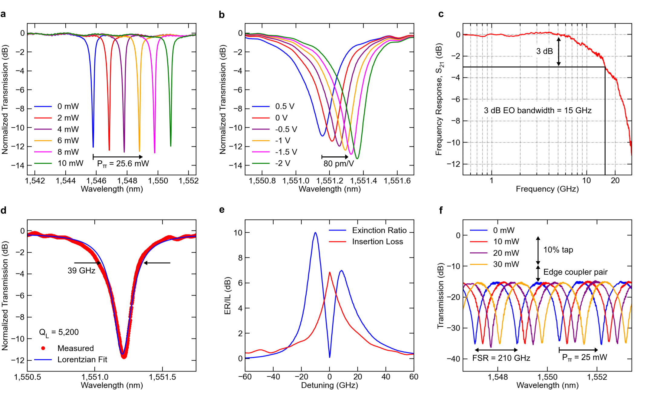
Integrated thermo-optic heaters in the microdisk modulators are used to tune each resonant wavelength to align to the target comb line. The modulators have an embedded vertical p-n junction which overlaps with the optical whispering gallery mode. When driven in reverse bias, the width of the depletion region is modulated which changes the free carrier distribution interacting with the optical mode and thus changes the effective refractive index through the plasma-dispersion effect. This change in the effective index corresponds to a shift in the resonant wavelength, which modulates the amplitude of the light to achieve levels of ‘0’ and ‘1’ depending on the applied bias. Due to the large overlap between the depletion region and optical mode in vertical junction devices Timurdogan2014 , the modulators can be directly driven at CMOS-compatible voltages while maintaining a high extinction ratio and low insertion loss (Fig. 3e). Furthermore, silicon photonic modulators based on the plasma-dispersion effect have been experimentally shown to function over hundreds of nanometres Doerr2016 and thus will not restrict the wavelength scalability of the system. For all data transmission experiments in this work, the modulators were driven at 1.3 Vpp, yielding an extinction ratio of 7 dB with an insertion loss of 3 dB (Fig. 3e).
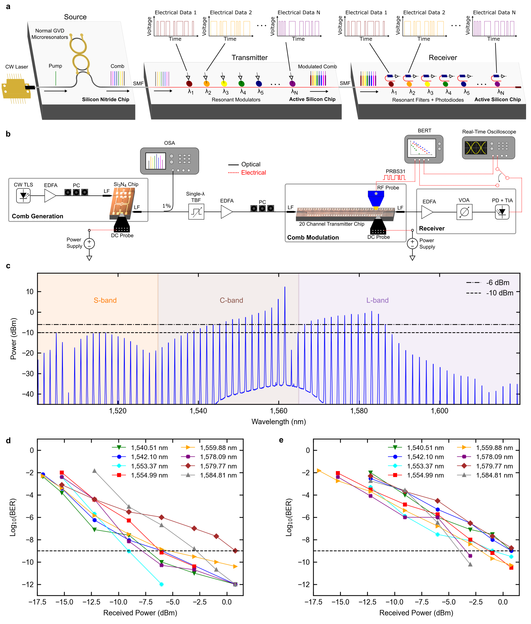
The source consists of a Si3N4 Kerr comb operating in the normal group velocity dispersion (GVD) regime which demonstrates higher conversion efficiency, power per line, and spectral flatness compared to soliton Kerr combs in the anomalous GVD regime Kim:19 ; jang2020 ; Fulop2018 ; Lobanov2015 ; Liu:14 ; Xue2015 , making normal-GVD combs better suited for data communication applications. The comb was designed to have 200 GHz spacing to operate in the ideal regime for bandwidth and conversion efficiency while maintaining high power-per-line. Similar devices have shown experimentally measured pump-to-comb conversion efficiencies up to 41% Kim:19 . The dual resonators have platinum heaters above the Si3N4 waveguide layer, enabling thermo-optic tuning of an avoided mode crossing to enable arbitrary pump wavelengths for generating the low-noise comb spectrum Kim:19 ; Miller:15 . To achieve the low-noise wavelength channels required for high fidelity data transmission, the resonances are tuned to generate a low-noise comb for all experiments (Supplementary Note 3). The fibre-coupled output spectrum of the comb is shown in Fig. 2c, demonstrating 25 lines above -6 dBm and 33 lines above -10 dBm. The output edge coupler loss on the Si3N4 chip was measured to be -3 dB, leading to 25 lines with on-chip power above -3 dBm.
To evaluate the performance of the single bus architecture with a microcomb source, we fabricated a transmitter chip with 20 cascaded microdisk modulators through the American Institute for Manufacturing (AIM) multi-project wafer (MPW) service (Methods) (Fig. 2b). Lensed fibre was used to couple the comb output to the transmitter chip input, which displayed a coupling loss of 5 dB/facet and thus required amplification before and after the transmitter. Multiple comb lines were sampled over 44.3 nm of spectral bandwidth in the C- and L-bands, with all eight lines achieving directly-measured bit error rates (BER) better than for 10 Gb/s/ and 16 Gb/s/ without the use of forward error correction (Fig. 2d,e).
Despite supporting modest DWDM channel counts, single bus cascaded resonator links run into fundamental scaling restrictions due to the limited free spectral range (FSR) of the resonators, constraining the usable bandwidth to a single FSR. To pack more channels into a single FSR, the channel spacing must be reduced; however, channel spacings below 100 GHz lead to severe crosstalk penalties kishore and thus place an upper bound on the number of allowable channels within a given FSR. To mitigate this restriction, we propose a scalable link architecture which sub-divides the comb to reduce the number of channels per bus and permits channel arrangements which are not restricted to a single resonator FSR Rizzo21 (Supplementary Note 4).
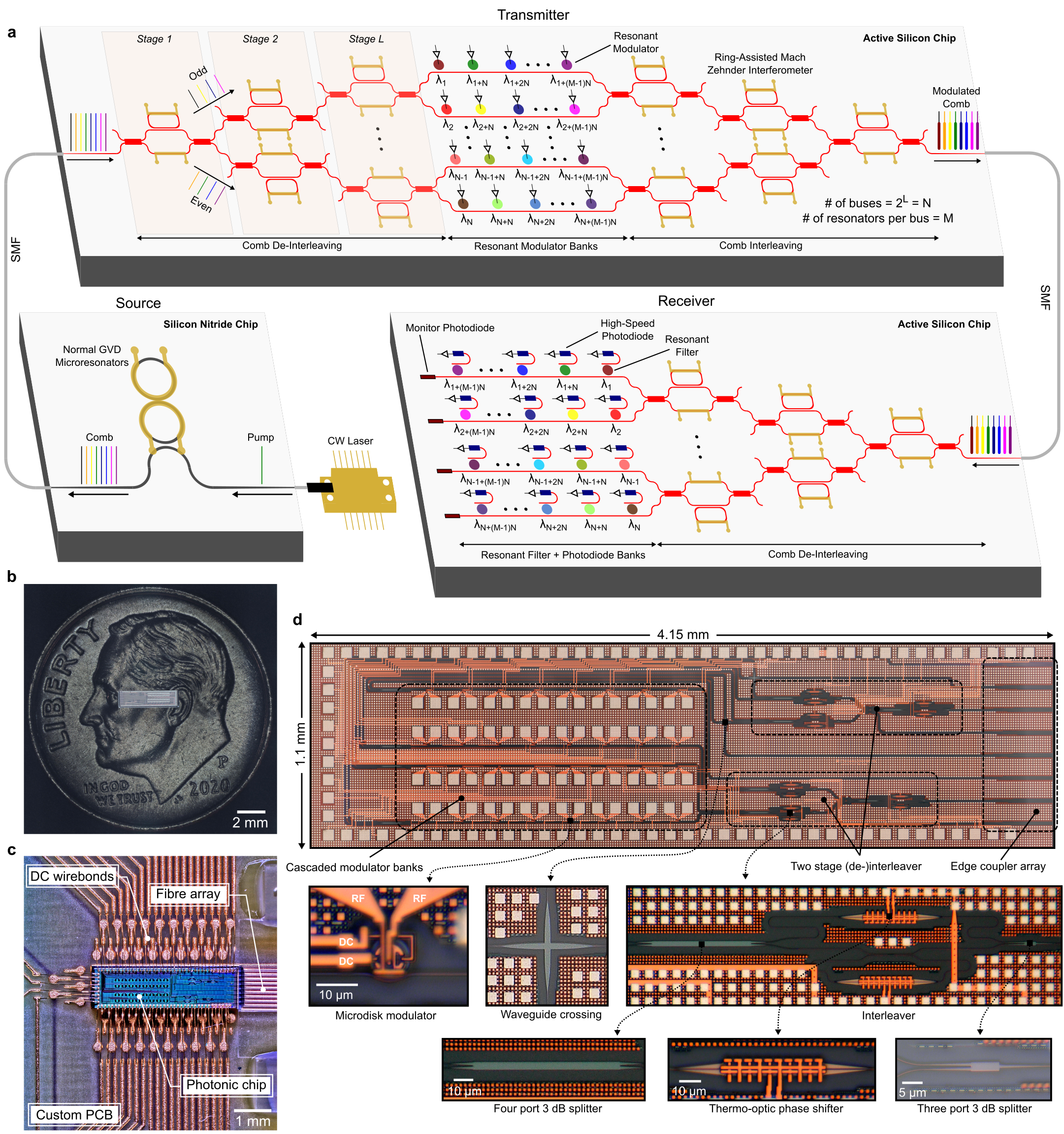
The proposed scalable link architecture is shown in Fig. 4a. The source consists of an external or integrated CW laser which pumps a Si3N4 dual-microresonator system to generate the normal-GVD comb source. Standard single mode fibre (SMF) is used to connect the source to the transmitter chip. The transmitter architecture uses a binary tree of asymmetric Mach Zehnder interferometers (MZI) to split the comb spectrum into even and odd groups at each stage. After the comb is divided into subgroups, the groups traverse separate buses of cascaded microdisk modulators, taking advantage of the spectral selectivity of resonant modulators to encode independent data streams onto different coloured comb lines. After each channel is modulated, they are recombined using an identical binary tree of MZIs and coupled off the chip into SMF. At the receiver, the modulated comb lines traverse a final MZI binary tree and are then incident on buses with cascaded resonant filters tuned to match the respective wavelength channels. Each resonant filter has a photodetector at its drop port to convert the optical data streams back into the electrical domain. This architecture naturally enables a disaggregated laser source, which allows the pump and comb to be separately stabilised away from the harsh thermal environment of co-packaged optics and electronics.
The binary trees of MZI filters serve multiple purposes—depending on the depth of the tree , the channel spacing on each bus is increased by a factor of . Additionally, the number of channels per bus is reduced by a factor of , enabling channel configuration schemes that are not restricted by the FSR of the resonant modulators/filters (Supplementary Note 4). Recently, a fully automated control algorithm for aligning similar cascaded MZI binary trees was demonstrated Akiyama:21 , providing a straightforward path to full-system initialisation and stabilisation.
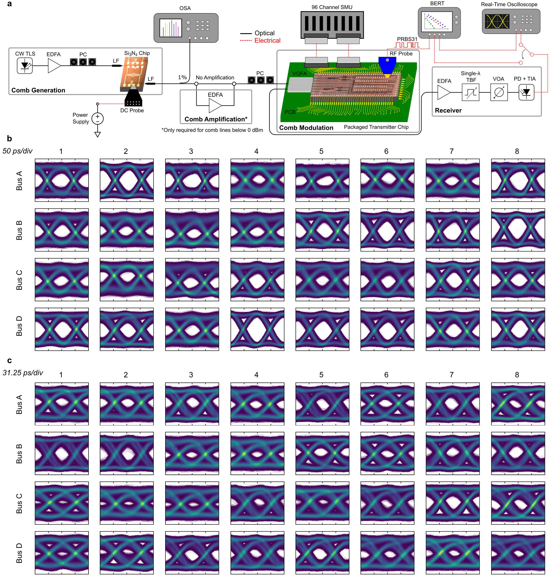
To verify the proposed architecture experimentally, we fabricated a 4.15 mm 1.1 mm photonic transmitter chip designed for 32 wavelength channels in a commercial 300 mm foundry through the AIM MPW service. The (de-)interleavers were implemented as asymmetric ring-assisted Mach Zehnder interferometers (RMZIs) which exhibit flatter pass- and stop-bands compared to standard asymmetric MZI filters Luo:10 ; Rizzo2021 . Two stages of de-interleavers were used to subdivide the comb into four groups which are incident on banks of eight cascaded microdisk modulators (Fig. 4d). After modulation, the groups are recombined onto a single fibre using two stages of RMZI interleavers. While the transmitter chip only requires a single fibre in and a single fibre out for data transmission, six ancillary optical I/O ports are used to tap the circuit at various points for (de-)interleaver and modulator alignment.
The photonic transmitter chip was optically packaged with an eight channel SMF array at 127 m pitch and electrically packaged for the DC thermal controls with 96 wirebonded pads around the periphery at 100 m pitch (Methods). The measured optical coupling loss after UV curing with index matching epoxy was 2.5 dB/facet, which greatly reduced the required optical power per line from the comb to close the link budget compared to the bare die case. Due to the high parasitic inductance of wirebonds, the inner high-speed radio frequency (RF) pads to the modulators were left exposed for probing with multi-contact wedge probes. All thermal biases were addressable with uniform current-voltage characteristics, indicating 100% yield for the DC wirebonds and photonic devices. Furthermore, all modulators on the chip displayed open eye diagrams up to 16 Gb/s (Fig. 5b,c), indicating uniform electro-optic bandwidth across devices (Fig. 3c) and 100% yield for the high speed photonic devices. The perfect yield and high device uniformity emphasise the advantage of fabrication in a commercial 300 mm CMOS foundry and bode well for the system’s potential for future high volume scaling.
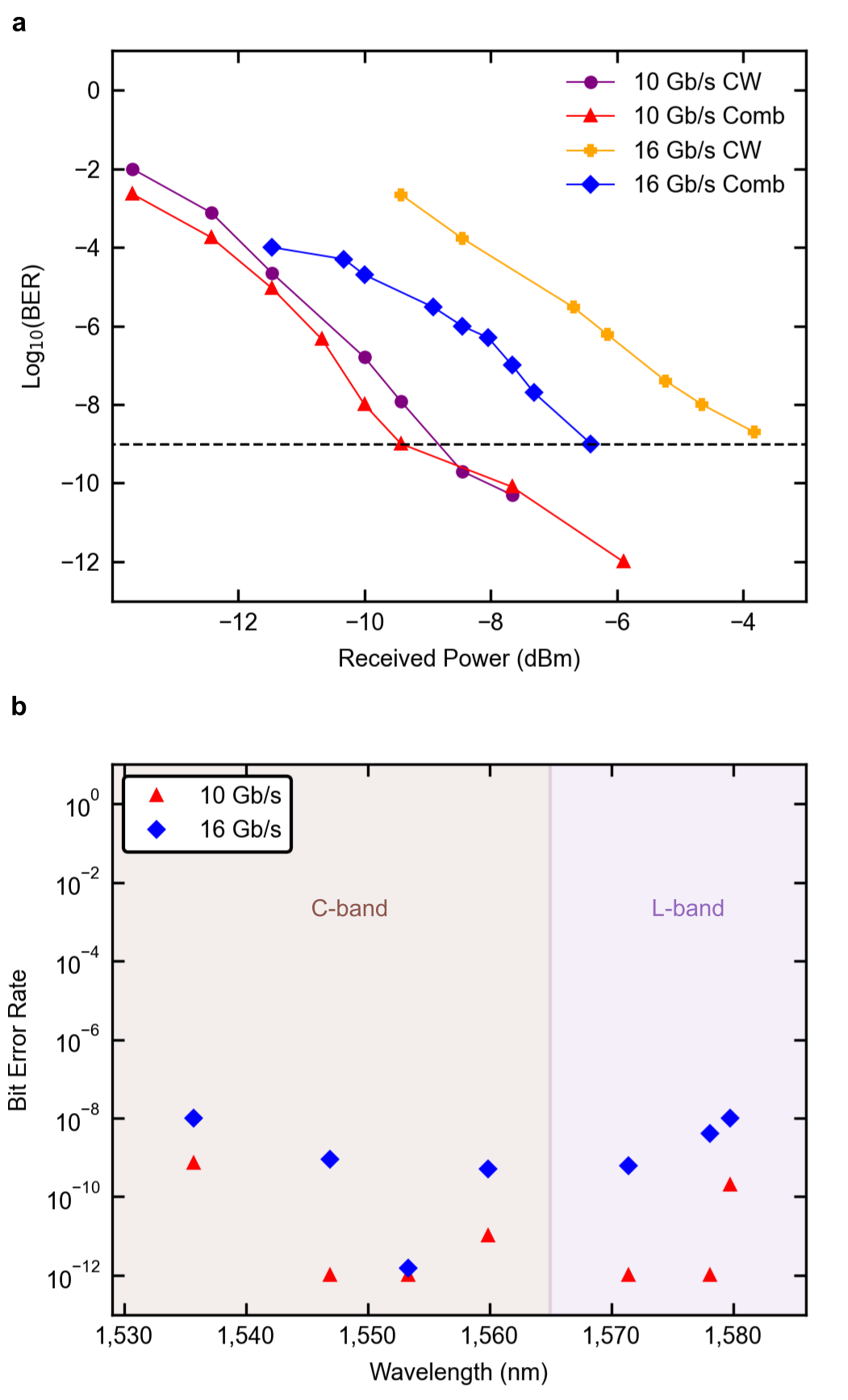
The individual comb lines showed a negligible power penalty compared to a tunable CW laser source and in some cases showed an improvement over the CW source (Fig. 6a). Due to the low coupling losses of the packaged transmitter chip and the low on-chip losses of the photonic devices, the comb line one channel blue detuned from the pump (1,559.8 nm) had enough fibre-coupled optical power to close the link budget without comb amplification prior to the transmitter chip (Fig. 6a). This result is promising for future link iterations with reduced fiber-chip coupling losses and integrated high sensitivity receiver modules Daudlin21 , as it shows that the generated comb lines can natively have enough optical power per line to close the link budget without the need for EDFAs (Supplementary Note 1).
To further verify the system performance, BER values were directly measured for sampled comb lines across the C- and L-bands (Fig. 6b). Due to the cascaded interleavers on the transmitter chip used for subdividing the comb, no filtering was required between the Si3N4 comb chip and the transmitter package. All off-chip filtering was restricted to the receiver-side, where a tunable filter was used to emulate resonant drop filters for selecting single modulated comb lines. At both 10 Gb/s and 16 Gb/s, all comb lines achieved BER values better than , with most lines below and some natively error-free ( ). With improved photonic devices, improved receiver sensitivity, and the elimination of noisy EDFAs, it is likely that every comb line across the S-, C-, and L-bands can achieve error-free performance based on their coherence and noise properties Kim:19 .
Discussion
In conclusion, we have demonstrated the first integrated photonic transmitter using a normal-GVD Kerr comb source operating at a state-of-the-art aggregate bandwidth through massively parallel DWDM. In contrast with other comparable high-bandwidth solutions which scale through increasing the single-channel baud rate and moving to higher-order modulation formats, our demonstrated approach permits modest per-channel data rates with a standard NRZ-OOK modulation format. This approach enables extreme energy efficiency and low latency through elimination of power-hungry DSP and FEC while still maintaining high aggregate bandwidths per fibre. We experimentally characterised data transmission up to 512 Gb/s on a single fibre (465 Gb/mm shoreline bandwidth density) with continued room for scaling through a novel link architecture. Moreover, normal-GVD Kerr combs inherently have high conversion efficiencies ( 30%) and recently have been shown to synchronize to produce comb line powers otherwise unattainable kim2021synchronization .
The transmitter chip was fabricated in a standard SOI process at a commercial foundry, enabling straightforward packaging with modern CMOS electronics for fully integrated transceivers either through heterogeneous Daudlin21 or monolithic global integration. Furthermore, this architecture enables continued scaling in the number of wavelength channels as well as per-channel data rate (with a trade-off in energy efficiency) with improved modulator designs Sun:19 and is fully compatible with other common multiplexing techniques such as mode-division multiplexing Oscar:20 ; yang2021inversedesigned ; Luo2014 . Additionally, recent work has shown automated wafer-scale trimming of resonant modulators to correct for fabrication variations intel2021 , enabling future as-designed alignment of modulators and filters to the comb grid without any thermal energy consumption.
Previous roadblocks to the use of Kerr combs for short-reach optical links have recently been overcome, with solutions for high volume manufacturability Jin2021 ; Liu2021 ; Xiang99 ; Ji:17 ; Ji:20 , high optical power per line with spectral flatness Jang2018 ; kim2021synchronization , high pump-to-comb conversion efficiency Xue2015 ; Kim:19 , and turn-key integration in standard compact laser packages Stern2018 ; Shen2020 . In concert with these advancements, the work presented here represents a coming-of-age for Kerr frequency combs as optical interconnect sources, establishing them as a pragmatic contender for integration in next-generation data centres and high performance computers.
Methods
Active Silicon Photonic Chip. The active silicon photonic circuit was designed using a mix of custom designed devices and verified process design kit (PDK) components provided by the foundry. Custom devices were designed using the Ansys Lumerical Finite Difference Time Domain (FDTD) Solver to extract S-parameters and create compact models which were then used to perform circuit-level simulations with the PDK devices in Ansys Lumerical INTERCONNECT. The mask layout was prepared in Cadence Virtuoso and physical verification was performed using Mentor Graphics Calibre. Fabrication was performed as part of the AIM Photonics 300 mm multi-project wafer service. The AIM process uses a 220 nm thick silicon waveguide layer with 2 m thick buried oxide. For a single-mode strip waveguide of nominal width (480 nm), the propagation loss is approximately 2.5 dB/cm. Additionally, the AIM process and PDK use Si3N4 layers for devices such as inverse-tapered edge couplers and silicon-to-Si3N4 escalators, indicating that monolithic integration of the comb-generating microresonators on the same die as the active silicon devices is a future possibility with improved foundry nitride processing. More information regarding the AIM process and PDK can be found in ref. AIMPDK .
Si3N4 Chip Fabrication and Design. Starting from a 4-inch silicon wafer, we thermally grow a 4-m thick oxide layer as the bottom cladding. Si3N4 is deposited using low-pressure chemical vapor deposition (LPCVD) in two steps and annealed at 1,200 °C in an argon atmosphere for 3 hours in between steps. After Si3N4 deposition, we deposit a SiO2 hard mask using plasma-enhanced chemical vapor deposition (PECVD). We pattern our devices using electron beam lithography. Ma-N 2403 resist was used to write the pattern and the nitride film was etched in an inductively coupled plasma reactive ion etcher (ICP RIE) using a combination of CHF3, N2, and O2 gases. After stripping the oxide mask, we anneal the devices again to remove residual N-H bonds in the Si3N4 film. We clad the devices with 500 nm of high-temperature silicon dioxide (HTO) deposited at 800 °C followed by 2 m of SiO2 using PECVD. A deep etched facet and an inverse taper are designed and used to minimize the edge coupling loss. More detailed information on the device fabrication can be found in refs. Ji:17 ; Ji:2021 . The coupled-microresonator system was designed to generate a 200 GHz-spaced comb and the cross-section of the Si3N4 microrings was 730 x 1,000 nm. Platinum heaters were implemented over both resonators to tune an avoided mode crossing for generating a normal-GVD comb with an arbitrary pump wavelength. More information regarding the turn-key operation and noise properties of a similar comb can be found in ref. Kim:19 .
Device Packaging. The electrical and optical packaging was performed by Optelligent, LLC. The active silicon photonic chip was first die-bonded to a co-designed printed circuit board (PCB). The PCB bond pads were finished with electroless nickel electroless palladium immersion gold (ENEPIG) to enable better bond reliability with gold wirebonds. All 96 DC pads around the periphery of the photonic chip were wirebonded to the PCB and the 64 internal RF pads were left exposed for probing. An 8-channel lidless v-groove fibre array with standard cleaved SMF-28 fibres (OZ Optics) was flipped upside down to provide clearance over the chip dicing trench and was attached to the 127 m pitch edge coupler array on the photonic chip using index matching UV-cured epoxy after active alignment. The measured optical coupling loss after packaging was approximately 2.5 dB per facet.
Modulator Characterisation. Microdisk modulators available in the AIM PDK AIMPDK were used for the transmitter with four nominal wavelength designs (1,550 nm, 1,556.4 nm, 1,562.8 nm, and 1,569.4 nm). The modulators each have an FSR of approximately 25.6 nm. Integrated thermal heaters in each modulator were used to shift the resonances to align to the comb wavelength grid, with a measured tuning efficiency of 0.5 nm/mW. Future iterations using custom modulator designs with more nominal wavelengths and high efficiency heaters will greatly reduce the expended thermal tuning power. The measured loaded quality factor (Q) of a typical modulator was 5,200 ( = 39 GHz at 1,550 nm) which indicates an optical 3 dB modulation bandwidth of GHz using the relation Timurdogan2014 ; Osgood2002 . The electro-optic 3 dB bandwidth was measured to be GHz with a 0 V DC bias (Fig. 3c) which is combined with the calculated optical modulation bandwidth to estimate the RC bandwidth through the relation , yielding GHz Timurdogan2014 .
Interleaver Characterisation and Alignment. The RMZI interleavers have a thermo-optic phase shifter in both the ring and bottom arm to correct for phase errors due to fabrication variations. An applied power of 25 mW to the bottom arm heater yields an FSR/2 shift of the pass- and stop-bands, corresponding to a phase shift. The first de-interleaver stage has a 10% power tap in the bottom arm which is looped back to an output edge coupler to align the pass- and stop-bands. A tunable laser (Keysight 81608A), lightwave measurement system (Keysight 8164B), and four channel optical power meters (Keysight N7744A) were used to sweep the (de-)interleaver spectrum while on-chip thermo-optic heaters were tuned to align the spectrum to the comb wavelength grid. Power taps were used at the end of each bus to similarly align the second stage de-interleaver and modulator resonances. A tap before the last interleaver stage was used for final alignment to recombine the comb onto a single fibre output.
Data Transmission Experiments. The Si3N4 comb chip was pumped using a tunable CW laser with 7 dBm output power (Alnair Labs TLG-200) which was amplified to 1 W using an erbium-doped fibre amplifier (EDFA) (Amonics AEDFA-33-B-FA). The polarisation of the pump was tuned with a polarisation controller ensure that the fundamental transverse electric (TE) mode was launched into the chip edge couplers. The edge couplers on the comb chip had a measured loss of 3 dB/facet, yielding 500 mW of on-chip optical power for comb generation. The generated comb was amplified using a broadband C- and L-band EDFA (FiberLabs AMP-FL8021-CLB-22) and was sent to the transmitter package using single-mode fibre with a polarisation controller to launch TE-polarised light into the chip. The transmitter PCB was mounted to a temperature-controlled stage (Thorlabs PTC1) to thermally stabilise the chip. DC biases for thermo-optic control of the interleavers and modulators were provided by a 96 channel source measurement unit (Qontrol) connected to the PCB. The bit pattern was generated by a bit-error rate tester (BERT) (Anritsu MP1900A) and was sent to the modulators using RF multi-contact wedge probes (Cascade Infinity). All data transmission experiments used a pseudo-random bit sequence of length (PRBS31) to provide the most rigorous test pattern and eliminate the possibility of pattern-dependent behaviour. After modulation, the light was coupled off the chip into single-mode fibre and amplified using a broadband C- and L-band EDFA (FiberLabs AMP-FL8021-CLB-22). A tunable bandpass filter (Finisar Waveshaper) was then used to select single modulated comb lines with a variable optical attenuator (Thorlabs EVOA1550A) to control the optical power to the receiver. The modulated comb lines were then converted back into the electrical domain using a photodiode and trans-impedance amplifier (Thorlabs RXM40AF). The received signal was sent to a real-time oscilloscope (Keysight Infiniium Z-Series) for eye characterisation or back to the BERT for bit-error rate evaluation.
Acknowledgements.
This work was supported in part by the U.S. Advanced Research Projects Agency–Energy under ENLITENED Grant DE-AR000843 and in part by the U.S. Defense Advanced Research Projects Agency under PIPES Grant HR00111920014. This work was performed in part at the Cornell NanoScale Facility, a member of the National Nanotechnology Coordinated Infrastructure (NNCI), which is supported by the National Science Foundation (Grant NNCI-2025233). The authors thank Paul Gaudette and David C. Scott (Optelligent, LLC) for device packaging, AIM Photonics for chip fabrication, Michael L. Fanto for assistance with chip imaging, and Analog Photonics for PDK support. Additionally, the authors acknowledge fruitful conversations with Xiang Meng, Nathan C. Abrams, Hao Yang, and Yu-Han Hung.Author Contributions
A.R. and Q.C. conceived the link architecture and performed initial calculations. A.R. performed the circuit simulations, designed the floorplan, and drew the top level mask layout. V.G. designed the PCB and conducted the DC electro-optic characterisation. B.Y.K. and Y.O. designed, simulated, and characterised the Kerr comb microresonators and X.J. fabricated the Si3N4 chip. A.N. led the high-speed testing and data transmission experiments with assistance from A.R., S.D., and V.G. All authors helped analyse the data and A.R. prepared the manuscript with input from all authors. M.L., A.L.G., and K.B. supervised the project.
Competing Interests
The authors declare no competing interests.
Data Availability
The data that support the plots within this paper and other findings of this study are available from the corresponding author upon reasonable request.
Correspondence
Correspondence and requests for materials should be addressed to K.B. (email: bergman@ee.columbia.edu).
References
- (1) Cheng, Q., Bahadori, M., Glick, M., Rumley, S. & Bergman, K. Recent advances in optical technologies for data centers: a review. Optica 5, 1354–1370 (2018).
- (2) Miller, D. Rationale and challenges for optical interconnects to electronic chips. Proceedings of the IEEE 88, 728–749 (2000).
- (3) Strubell, E., Ganesh, A. & McCallum, A. Energy and policy considerations for deep learning in nlp. arXiv:1906.02243 (2019).
- (4) Miller, D. A. B. Device requirements for optical interconnects to silicon chips. Proceedings of the IEEE 97, 1166–1185 (2009).
- (5) Miller, D. A. B. Attojoule optoelectronics for low-energy information processing and communications. Journal of Lightwave Technology 35, 346–396 (2017).
- (6) Sun, C. et al. Single-chip microprocessor that communicates directly using light. Nature 528, 534–538 (2015).
- (7) Atabaki, A. H. et al. Integrating photonics with silicon nanoelectronics for the next generation of systems on a chip. Nature 556, 349–354 (2018).
- (8) Hu, H. & Oxenløwe, L. K. Chip-based optical frequency combs for high-capacity optical communications. Nanophotonics 10, 1367–1385 (2021).
- (9) Gaeta, A. L., Lipson, M. & Kippenberg, T. J. Photonic-chip-based frequency combs. Nature Photonics 13, 158–169 (2019).
- (10) Levy, J. S. et al. Cmos-compatible multiple-wavelength oscillator for on-chip optical interconnects. Nature Photonics 4, 37–40 (2010).
- (11) Levy, J. S. et al. High-performance silicon-nitride-based multiple-wavelength source. IEEE Photonics Technology Letters 24, 1375–1377 (2012).
- (12) Kippenberg, T. J., Gaeta, A. L., Lipson, M. & Gorodetsky, M. L. Dissipative kerr solitons in optical microresonators. Science 361 (2018).
- (13) Marin-Palomo, P. et al. Microresonator-based solitons for massively parallel coherent optical communications. Nature 546, 274–279 (2017).
- (14) Pfeifle, J. et al. Coherent terabit communications with microresonator kerr frequency combs. Nature Photonics 8, 375–380 (2014).
- (15) Fülöp, A. et al. High-order coherent communications using mode-locked dark-pulse kerr combs from microresonators. Nature Communications 9, 1598 (2018).
- (16) Kong, D. et al. Single dark-pulse kerr comb supporting 1.84 pbit/s transmission over 37-core fiber. In Conference on Lasers and Electro-Optics, JTh4A.7 (Optical Society of America, 2020).
- (17) Hu, H. et al. Single-source chip-based frequency comb enabling extreme parallel data transmission. Nature Photonics 12, 469–473 (2018).
- (18) Corcoran, B. et al. Ultra-dense optical data transmission over standard fibre with a single chip source. Nature Communications 11, 2568 (2020).
- (19) Wade, M. et al. Teraphy: A chiplet technology for low-power, high-bandwidth in-package optical i/o. IEEE Micro 40, 63–71 (2020).
- (20) Liang, D. et al. Integrated green dwdm photonics for next-gen high-performance computing. In Optical Fiber Communication Conference (OFC) 2020, Th1E.2 (Optical Society of America, 2020).
- (21) Chen, C.-H. et al. A comb laser-driven dwdm silicon photonic transmitter based on microring modulators. Opt. Express 23, 21541–21548 (2015).
- (22) Moscoso-Mártir, A. et al. Silicon photonics transmitter with soa and semiconductor mode-locked laser. Scientific Reports 7, 13857 (2017).
- (23) Zheng, X. et al. A 33mw 100gbps cmos silicon photonic wdm transmitter using off-chip laser sources. In Optical Fiber Communication Conference/National Fiber Optic Engineers Conference 2013, PDP5C.9 (Optical Society of America, 2013).
- (24) Liu, S. et al. High-channel-count 20 ghz passively mode-locked quantum dot laser directly grown on si with 4.1 tbit/s transmission capacity. Optica 6, 128–134 (2019).
- (25) Wang, C. et al. Monolithic lithium niobate photonic circuits for kerr frequency comb generation and modulation. Nature Communications 10, 978 (2019).
- (26) Xu, Q., Schmidt, B., Shakya, J. & Lipson, M. Cascaded silicon micro-ring modulators for wdm optical interconnection. Opt. Express 14, 9431–9436 (2006).
- (27) London, Y. et al. Energy efficiency analysis of comb source carrier-injection ring-based silicon photonic link. IEEE Journal of Selected Topics in Quantum Electronics 26, 1–13 (2020).
- (28) Bogaerts, W. et al. Silicon microring resonators. Laser & Photonics Reviews 6, 47–73 (2012).
- (29) Novick, A. et al. Error-free kerr comb-driven sip microdisk transmitter. In 2020 Conference on Lasers and Electro-Optics (CLEO), STu2B.5 (Optical Society of America, 2021).
- (30) Timurdogan, E. et al. An ultralow power athermal silicon modulator. Nature Communications 5, 4008 (2014).
- (31) Doerr, C. et al. O, e, s, c, and l band silicon photonics coherent modulator/receiver. In 2016 Optical Fiber Communications Conference and Exhibition (OFC), 1–3 (2016).
- (32) Kim, B. Y. et al. Turn-key, high-efficiency kerr comb source. Opt. Lett. 44, 4475–4478 (2019).
- (33) Jang, J. K. et al. Conversion efficiency of soliton kerr combs. Opt. Lett. 46, 3657–3660 (2021).
- (34) Lobanov, V. E., Lihachev, G. & Gorodetsky, M. L. Generation of platicons and frequency combs in optical microresonators with normal GVD by modulated pump. EPL (Europhysics Letters) 112, 54008 (2015).
- (35) Liu, Y. et al. Investigation of mode coupling in normal-dispersion silicon nitride microresonators for kerr frequency comb generation. Optica 1, 137–144 (2014).
- (36) Xue, X. et al. Mode-locked dark pulse kerr combs in normal-dispersion microresonators. Nature Photonics 9, 594–600 (2015).
- (37) Miller, S. A. et al. Tunable frequency combs based on dual microring resonators. Opt. Express 23, 21527–21540 (2015).
- (38) Padmaraju, K., Zhu, X., Chen, L., Lipson, M. & Bergman, K. Intermodulation crosstalk characteristics of wdm silicon microring modulators. IEEE Photonics Technology Letters 26, 1478–1481 (2014).
- (39) Rizzo, A. et al. Kerr comb-driven silicon photonic transmitter. In Optical Fiber Communication Conference (OFC) 2021, Th4A.5 (Optical Society of America, 2021).
- (40) Akiyama, T. et al. Cascaded amz triplets: a class of demultiplexers having a monitor and control scheme enabling dense wdm on si nano-waveguide pics with ultralow crosstalk and high spectral efficiency. Opt. Express 29, 7966–7985 (2021).
- (41) Luo, L.-W. et al. High bandwidth on-chip silicon photonic interleaver. Opt. Express 18, 23079–23087 (2010).
- (42) Rizzo, A., Cheng, Q., Daudlin, S. & Bergman, K. Ultra-broadband interleaver for extreme wavelength scaling in silicon photonic links. IEEE Photonics Technology Letters 33, 55–58 (2021).
- (43) Daudlin, S. et al. 3d-integrated multichip module transceiver for terabit-scale dwdm interconnects. In Optical Fiber Communication Conference (OFC) 2021, Th4A.4 (Optical Society of America, 2021).
- (44) Kim, B. Y. et al. Synchronization of non-solitonic kerr combs. arXiv:2104.15141 (2021).
- (45) Giewont, K. et al. 300-mm monolithic silicon photonics foundry technology. IEEE Journal of Selected Topics in Quantum Electronics 25, 1–11 (2019).
- (46) Sun, J. et al. A 128 gb/s pam4 silicon microring modulator with integrated thermo-optic resonance tuning. J. Lightwave Technol. 37, 110–115 (2019).
- (47) Gordillo, O. A. J., Dave, U. D. & Lipson, M. Bridging between si and few-mode fiber higher order modes. In Conference on Lasers and Electro-Optics, SM2O.6 (Optical Society of America, 2020).
- (48) Yang, K. Y. et al. Inverse-designed multi-dimensional silicon photonic transmitters. arXiv:2103.14139 (2021).
- (49) Luo, L.-W. et al. Wdm-compatible mode-division multiplexing on a silicon chip. Nature Communications 5, 3069 (2014).
- (50) Jayatilleka, H. et al. Post-fabrication trimming of silicon photonic ring resonators at wafer-scale. Journal of Lightwave Technology 39, 5083–5088 (2021).
- (51) Jin, W. et al. Hertz-linewidth semiconductor lasers using cmos-ready ultra-high-q microresonators. Nature Photonics (2021).
- (52) Liu, J. et al. High-yield, wafer-scale fabrication of ultralow-loss, dispersion-engineered silicon nitride photonic circuits. Nature Communications 12, 2236 (2021).
- (53) Xiang, C. et al. Laser soliton microcombs heterogeneously integrated on silicon. Science 373, 99–103 (2021).
- (54) Ji, X. et al. Ultra-low-loss on-chip resonators with sub-milliwatt parametric oscillation threshold. Optica 4, 619–624 (2017).
- (55) Ji, X. et al. Exploiting ultralow loss multimode waveguides for broadband frequency combs. Laser & Photonics Reviews 15, 2000353 (2021).
- (56) Jang, J. K. et al. Synchronization of coupled optical microresonators. Nature Photonics 12, 688–693 (2018).
- (57) Stern, B., Ji, X., Okawachi, Y., Gaeta, A. L. & Lipson, M. Battery-operated integrated frequency comb generator. Nature 562, 401–405 (2018).
- (58) Shen, B. et al. Integrated turnkey soliton microcombs. Nature 582, 365–369 (2020).
- (59) Fahrenkopf, N. M. et al. The aim photonics mpw: A highly accessible cutting edge technology for rapid prototyping of photonic integrated circuits. IEEE Journal of Selected Topics in Quantum Electronics 25, 1–6 (2019).
- (60) Ji, X., Roberts, S., Corato-Zanarella, M. & Lipson, M. Methods to achieve ultra-high quality factor silicon nitride resonators. APL Photonics 6, 071101 (2021).
- (61) Gheorma, I.-L. & Osgood, R. Fundamental limitations of optical resonator based high-speed eo modulators. IEEE Photonics Technology Letters 14, 795–797 (2002).
See pages ,1,,2,,3,,4,,5,,6,,7,,8,,9 of Supplementary_Information_for_Integrated_Kerr_frequency_comb_driven_silicon_photonic_transmitter