Discretization of Annular-Ring Diffraction Pattern for Large-Scale Photonics Beamforming
Abstract
A solid-state active beamformer based on the annular-ring diffraction pattern is proposed for an integrated photonic platform. Such a circularly symmetric annular-ring aperture achieves radiating element limited FOV. Furthermore, it is demonstrated that a multi-annular-ring aperture with a fixed linear density of elements maintains the beam efficiency for larger apertures while reducing the beamwidth and side-lobe-level (SLL). A -element multi-annular-ring OPA with active beamforming is implemented in a standard photonics process. phase and amplitude modulators enable beamforming and beam steering using this aperture. A row-column drive methodology reduces the required electrical drivers by more than a factor of 5.
1 Introduction
Integrated solid-state photonic beamformers (optical phased arrays or OPAs) have the potential to reduce the cost, size, and implementation complexity of many photonic systems compared to their bulk optics and MEMS counterparts [1, 2]. These solid-state beamformers have been recently demonstrated for LiDAR [3, 4], photonic beam steering [5, 6, 7], medical imaging [8], and remote sensing [9] applications. In particular, standard silicon photonics processes can further reduce the cost and increase the yield and reliability of such systems [6, 10, 11, 12]. However, there are several challenges associated with the realization of large-scale solid-state beamformers.
Most integrated photonic dielectric waveguides and radiators have a minimum size and spacing on the order of the wavelength. This leads to minimum pitch and spacing constraints that lead to reduced field-of-view (FOV) and increased grating lobes as the size of the array aperture increases. There are two categories of architectures that have been utilized to overcome this problem. One class of architectures uses a wavelength-sensitive 1D-grid array of radiating elements to steer the beam in one direction and sweep the wavelength of the laser to steer the beam in the perpendicular direction [10, 11, 13, 14, 15]. This method removes the planar routing restriction at the cost of increased laser source and system complexity. Typically, a broadly tunable laser source (around of wavelength tunability) is required to achieve a moderate FOV (around ) [16, 17, 14]. Such tunable lasers are more complex and hence more costly compared to their single wavelength counterparts. Furthermore, such OPAs cannot offer wavefront control in the steering direction controlled by the wavelength.
Another class of architectures utilizes sparse array synthesis techniques to construct a 2D-grid array of radiating elements that permit routing the signals of the inner elements of the array [6]. Compared to their equal-size aperture, half-wavelength spacing counterparts, sparse arrays reduce the number of the radiating elements and phase shifters required, thus reducing array control complexity, power consumption, heat dissipation, and system cost. Furthermore, such arrays can operate with a fixed-wavelength laser source. These 2D-grid OPAs are advantageous over their 1D-grid aperture counterparts since they can offer full wavefront control with a fixed-wavelength laser. However, sparse placement of the elements reduces the array gain and beam efficiency (also known as the "sparse array curse"). Furthermore, most sparse array synthesis techniques achieve target beam performance by the randomized placement of elements in a 2D grid given the constraints on the number of elements and planar signal routing. For example, genetic algorithms have been used for sparse array synthesis [6, 18, 19]. This optimization process is computationally expensive for larger aperture sizes with an increased number of elements and there is no guarantee of arriving at the optimal design.
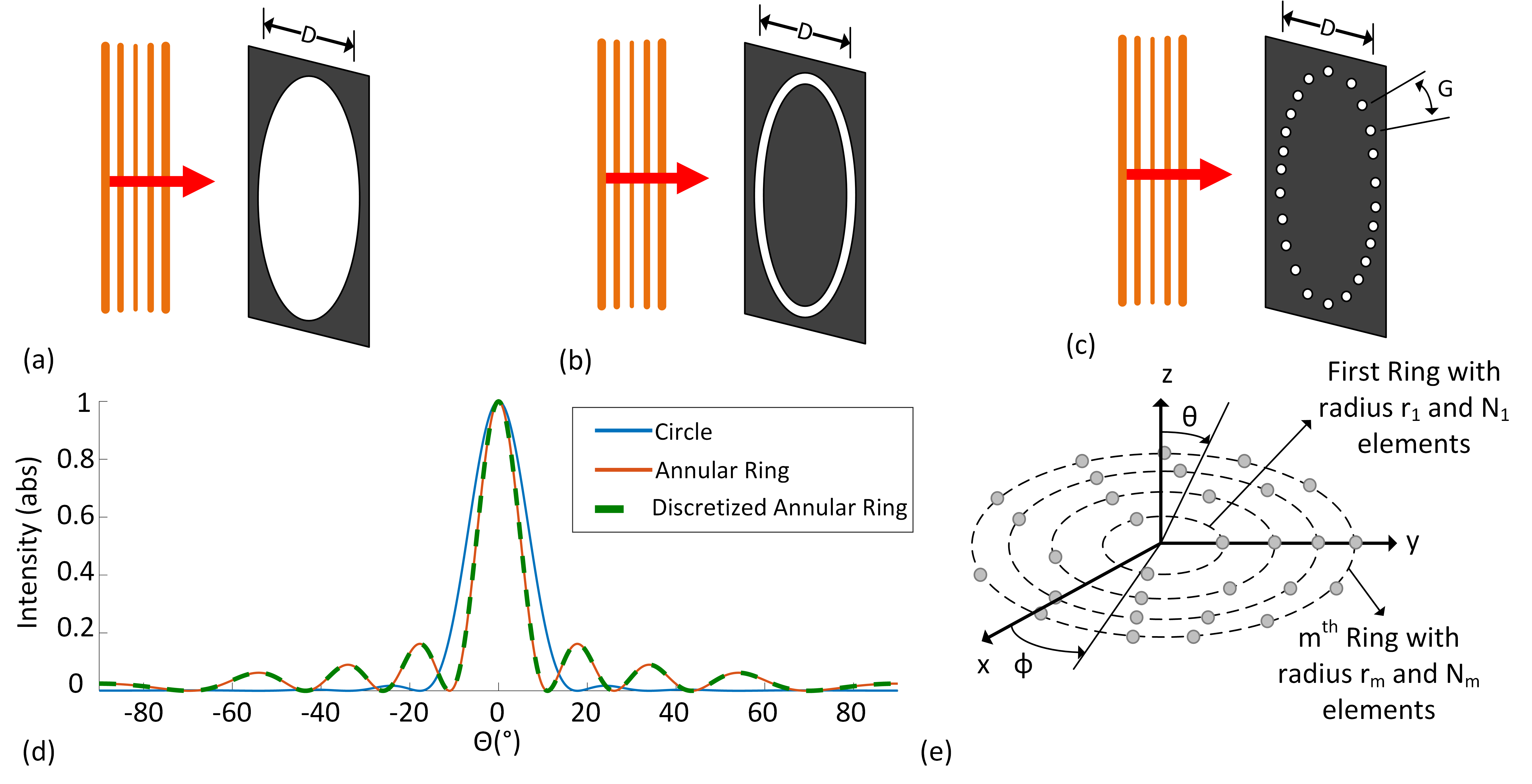
One method to reduce the complexity of finding optimum sparse apertures is to take advantage of the basic properties of circularly symmetric apertures. The ideal symmetric aperture is circular, as shown in Fig. 1(a). The beam pattern of such an aperture can be computed by taking the Fourier transform of a circle:
| (1) |
where is the radiation pattern, is the elevation angle, is the diameter of the circle, is the wave number and is the first order Bessel function of the first kind. The beam intensity cross-section of such aperture is shown in Fig. 1(d), as is described by function . Another circularly symmetric aperture is the annular-ring aperture (Fig. 1(b)), which can be modeled by blocking the center region of a circular aperture. The far-field beam pattern for such an aperture is given by the Fourier transform of difference of two circular apertures of diameter and , where is small:
| (2) |
where is the zeroth order Bessel function of first kind.
The beam intensity of this cross-section is shown in Fig. 1(d).
These beam patterns show that annular-ring apertures reduce the beamwidth at the cost of increased side-lobe level (SLL) compared to their circular counterparts that have an aperture with a significantly larger area. More importantly, annular-ring apertures do not produce grating lobes. This annular-ring aperture can be realized in a planar photonics process. We can physically implement an OPA capable of active beam steering by placing radiating elements on this annular ring at half-wavelength spacing 1(c). This discretized annular-ring array pattern approximates to the pattern of a continuous annular-ring aperture 1(d) for sufficiently large number of elements. It is possible to combine multiple such discretized annular rings to improve OPA beamwidth and SLL, as shown in Fig. 1(e). In phased array theory, such multi-annular-ring apertures can be categorized under circular-aperture arrays [20, 21, 22, 23, 24, 25]. Such symmetric apertures are advantageous over their rectangular counterparts since they exhibit minimal disturbance to the beamwidth and SLL when scanned azimuthally over the entire plane [26].
In this paper, we present the first demonstration of such OPAs in a silicon photonics platform. In the next section, we analyze the beamforming characteristics of such annular rings in the context of planar photonics platforms. Afterwards, we present a 255-element silicon photonics implementation of such an annular-ring OPA with full amplitude and phase control for individual radiators. We simplify the electrical drive interconnect complexity of such an OPA by using a row-column drive which reduces the total number of electrical interconnects from 510 nodes to 100 nodes. Finally, we discuss the beamforming optimization methodology of this large-scale OPA and demonstrate the beamforming and beam steering capability of this OPA.
2 Analysis of Annular-Ring Apertures
The discretized multi-annular-ring aperture can be generalized by creating concentric rings, each with isotropic radiators equidistant in arc length, where (Fig. 1(e)). Using the expression for the far-field radiation pattern or array factor of a single annular-ring aperture from [20], we can write the generalized array factor for a multi-annular-ring aperture as
| (3) |
where is the -field intensity for the particular element, is the radius of the th ring, is the angular position of the th element in the aperture, and pair describes the direction of the main beam. While amplitude apodization will help with SLL reduction, we limit this analysis to uniform excitation, , in the broad-side direction, .
2.1 Approximation of Continuous Annular-Ring Aperture
Using (3), we can compute the diffraction pattern of the continuous annular-ring aperture in Fig. 1(b) by assuming and replacing summation of the discrete points by integration over the entire circumference.
| (4) |
After normalizing (4), the beam pattern is a Bessel function of order zero similar to the diffraction pattern calculation for an annular ring in (2).
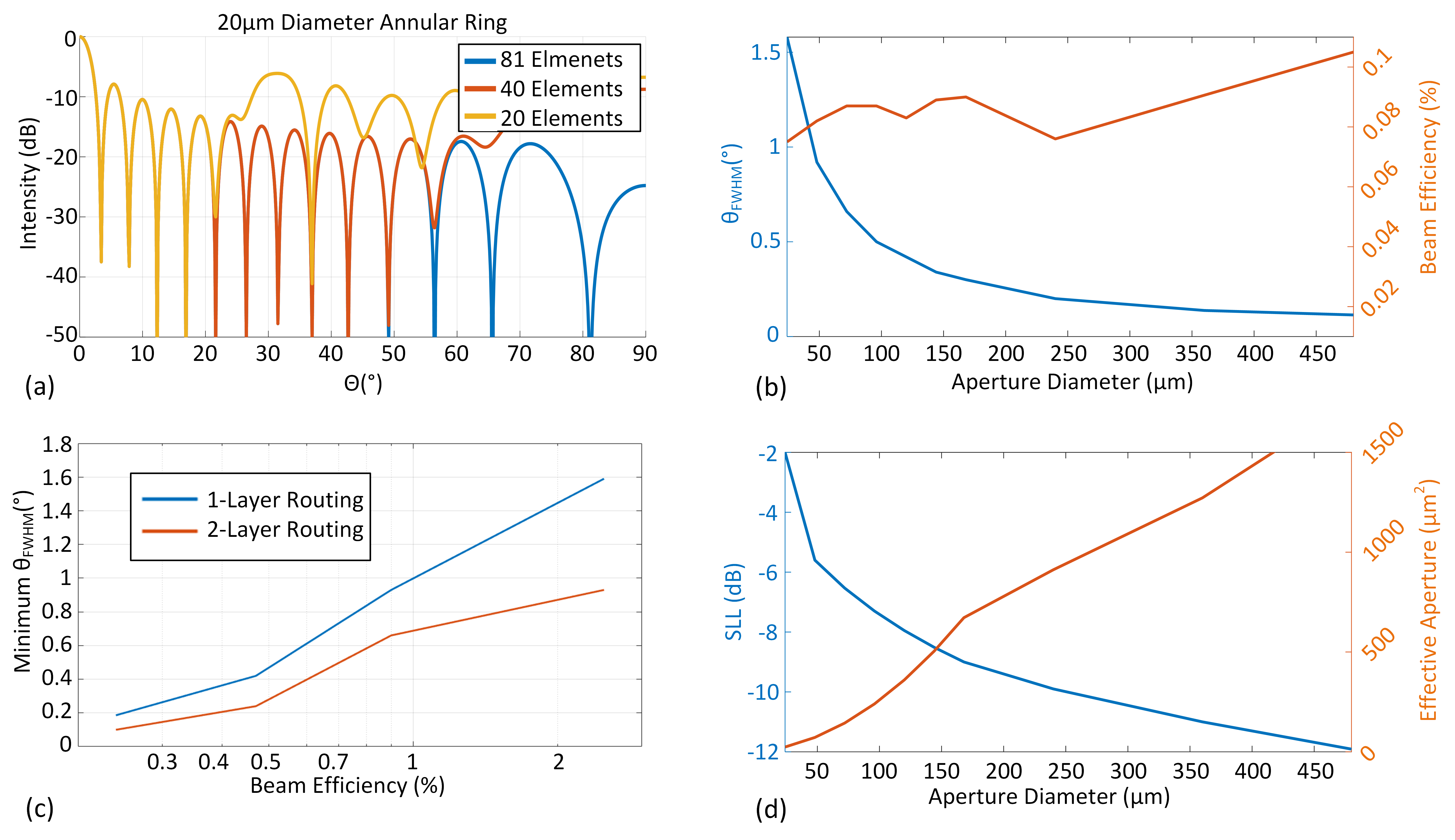
As shown in Fig. 1(d), placing discretized elements at distances up to half-wavelength spacing is equivalent to the continuous case with a Bessel function beam pattern. If the distance (over the arc) between the radiating elements increases to larger values, the Bessel function approximation holds for a narrower FOV. This is depicted in Fig. 2(a). Here, an annular-ring aperture with diameter and wavelength is plotted for continuous/half-wavelength case ( elements), , and radiating elements. For the case of radiating elements ( arc length spacing), the Bessel approximation is valid up to . For the case of radiating elements ( arc length spacing), the Bessel approximation is valid for up to . Furthermore, as the arc length spacing increase, the SLL increases.
2.2 Annular-Ring Apertures with a Fixed Linear Density
This multi-annular-ring aperture given by (3) is circularly symmetric, and as a result, the placement of the radiating elements can be optimized for desired performance parameters with reduced computational complexity compared to their rectangular grid sparse apertures. Such multi-annular-ring apertures can be analyzed for any of the beamforming parameters such as beamwidth, SLL, beam efficiency ( beam power over total radiated power), and element count. In this work, we limit our analysis of annular-ring apertures to apertures with fixed linear density. In other words, we assume a constant elements per arc length density () and linearly increase the ring radii ().
For such apertures with linear density, the planar photonic process parameters set the elements per arc length density as well as the minimum radius limits. For silicon photonics processes, the waveguides are typically wide with a minimum pitch of to reduce the electromagnetic coupling between the adjacent waveguides. Radiating elements can also be constructed at the size of the waveguides. For a fixed linear density, the design values and set the beam efficiency of the aperture. Assuming and , we can plot the beamwidth, beam efficiency, SLL, and effective aperture (total area of radiating elements) for different aperture sizes (values of ). Fig. 2(b) shows that while the half beamwidth decreases for larger and larger apertures, the beam efficiency remains relatively constant. Furthermore, Fig. 2(d) shows that SLL decreases as the aperture size gets larger and the effective aperture size also increases. Thus, multi-annular-ring apertures are good candidates for sparse phased-array receiver applications where collection area and SLL are important performance metrics. Moreover, these plots suggest that for a given pair, the beam performance improves while the beam efficiency remains constant. This provides a design methodology for multi-annular-ring apertures. We can proceed and calculate the largest apertures that can be constructed using these linear density annular-ring apertures. Assuming the waveguide and radiator size and pitch limitations of silicon photonics platforms mentioned above, we can plot the minimum achievable beamwidth for a given beam efficiency for single-layer and two-layer photonic platforms, as shown in Fig. 2(c). Thus, a multi-annular-ring OPA implemented in a single layer photonic platform with beam efficiency can resolve 9,300 points over the entire FOV. A two-layer photonic platform with the same efficiency approximately doubles the number of resolvable points to 18,500 in the far-field.
3 Multi-Annular-Ring OPA Implementation
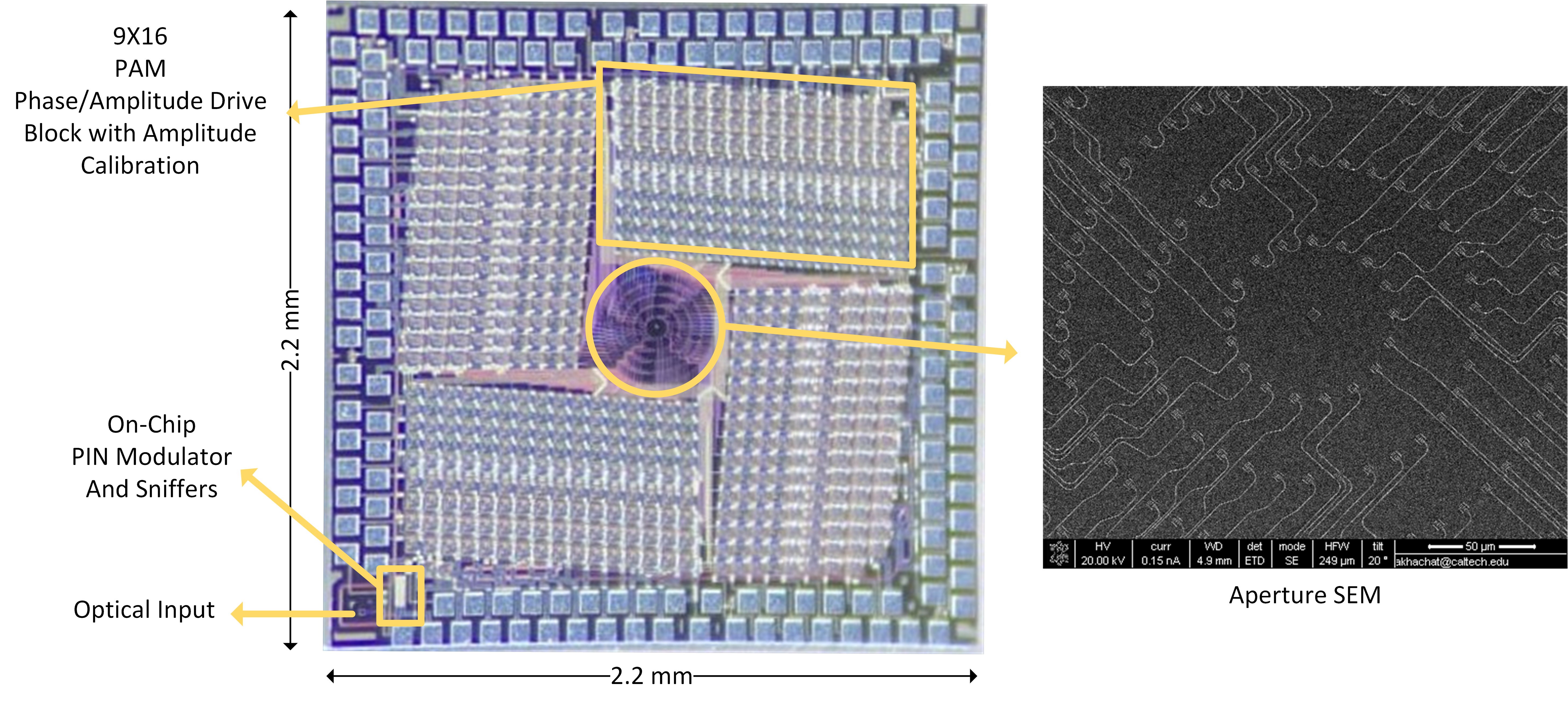
To demonstrate the beamforming and beam steering capability of multi-annular-ring aperture OPAs, we implemented a five-annular-ring aperture OPA system with active beamforming in Advanced Micro Foundry’s (AMF) standard photonics process. The die photo of this system is shown in Fig. 3. This OPA has a diameter annular-ring aperture with 255 radiating elements with complete phase and amplitude control. The thermo-optic phase and amplitude modulators are distributed into four blocks and electrically connected in a row-column fashion to reduce the electrical interconnect density from order to order . Amplitude modulation is achieved via a tunable amplitude distribution network which can be calibrated with only integrated sniffer photodiodes. The design details of these three sub-blocks are examined in the following sub-sections.
3.1 Implemented Aperture
This multi-annular-ring OPA array factor was optimized based on a minimum pitch in the waveguide routing with compact photonics radiators (Fig. 4(c)). Based on the analysis in section 2.2, we incorporated a five-annular-ring () aperture with a linear density ( and ). As a result, , and radiators are placed on rings with respective radii of , and , as shown in Fig. 4(a). This multi-annular-ring aperture maintains the Bessel form for a FOV with theoretical beamwidth with no grating lobes in the full FOV. The cross-section of the radiation pattern for this OPA is shown in Fig. 4(b).
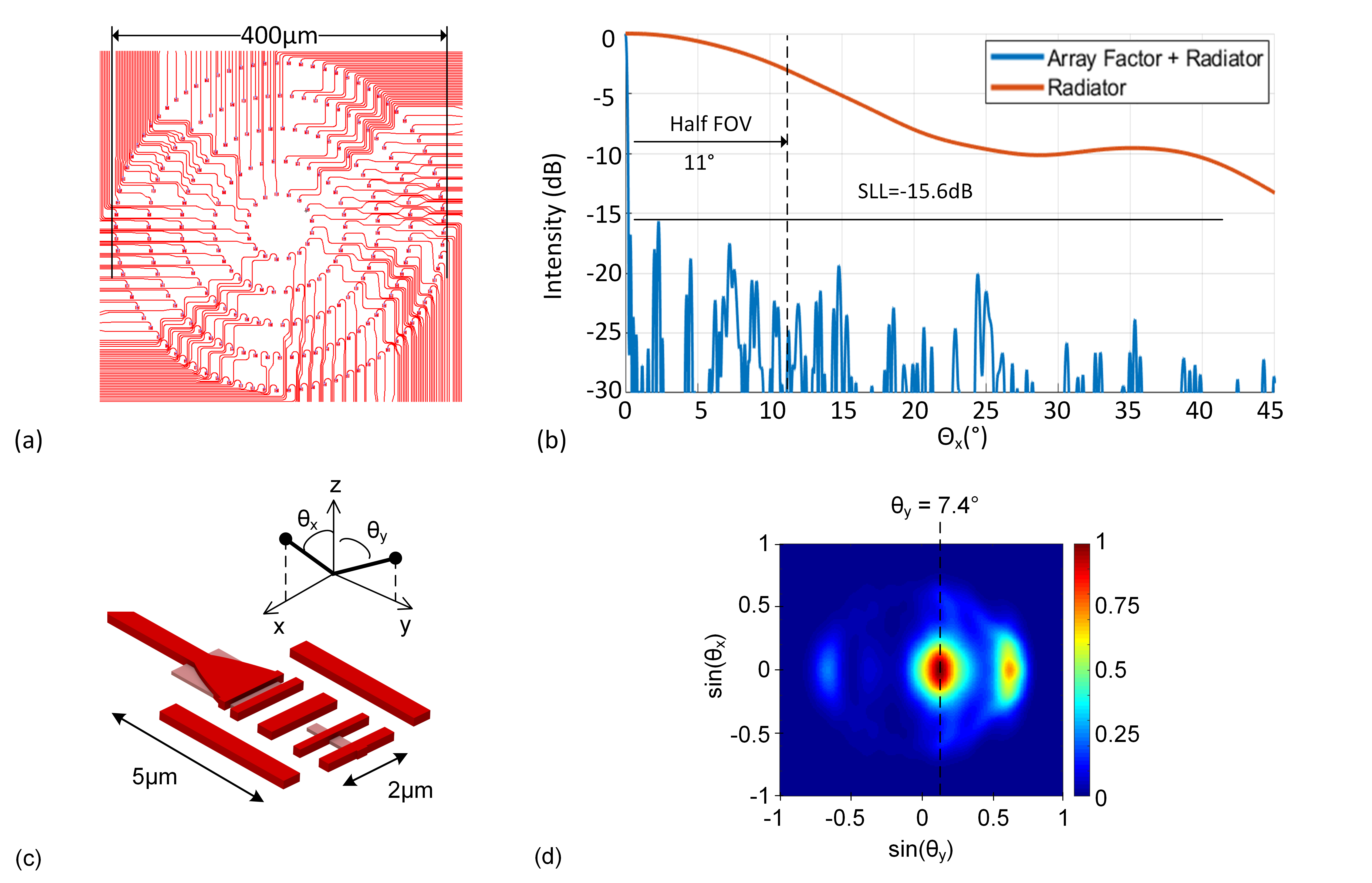
The radiating element used in this aperture has a far-field beamwidth of with over peak radiation efficiency at the optimum angle of [27]. Furthermore, the spectral bandwidth of the radiator is more than , which makes these radiators insensitive to temperature and wavelength variations. As a result, the FOV of this aperture is limited by the FOV of the radiating element with a maximum SLL of as shown in Fig. 4(b). Furthermore, the theoretical resolution of this OPA is total points.
3.2 Row-Column Drive
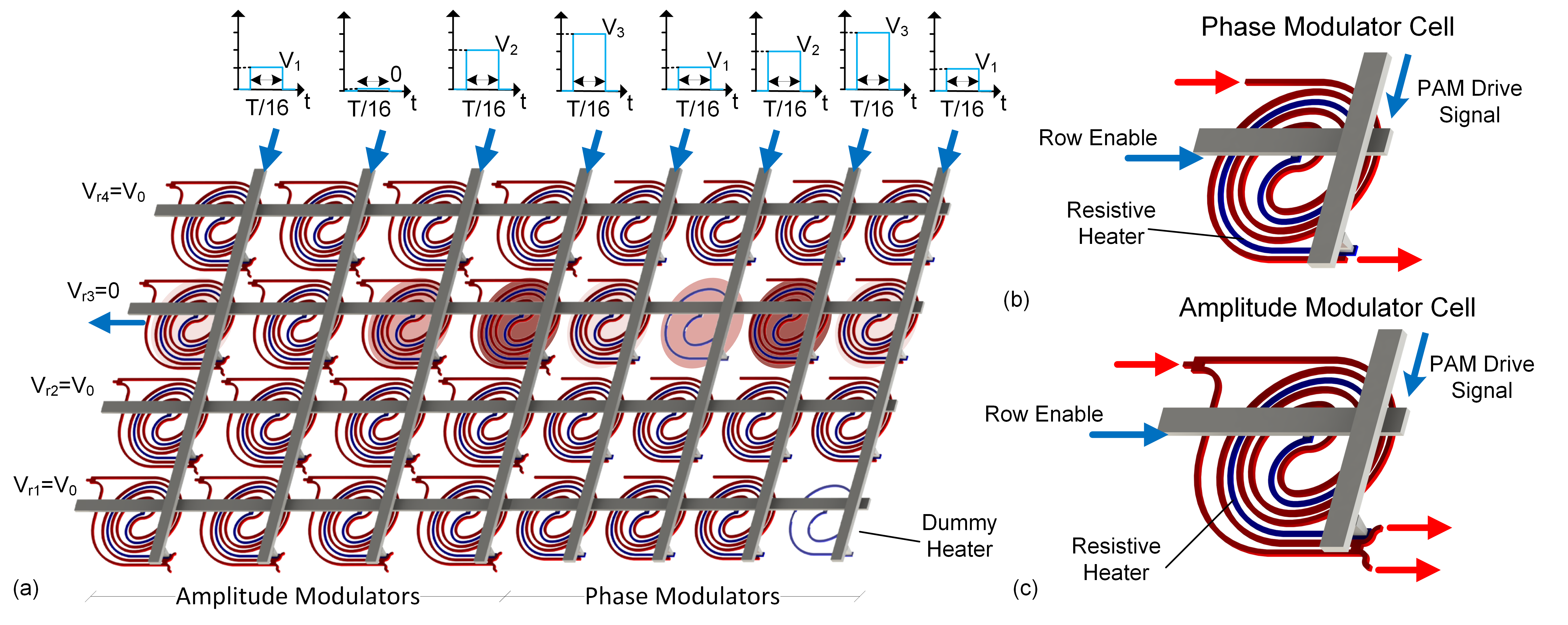
The amplitude and phase modulators for the 255-element array are divided into four blocks. Both amplitude and phase modulators incorporate a compact spiral thermo-optic phase shifter design to reduce the device footprint and increase isolation between radiating elements [27] as shown in Fig. 5(b)-(c). The amplitude modulation is achieved by a cascade of tunable optical couplers that split the light into 64 branches. This tunable power splitter requires tunable couplers. The output of each tunable coupler passes through phase shifters before reaching the radiating elements to adjust the relative phase between elements. These active components are electrically connected in a row-column fashion, as shown in Fig. 5(a). The tunable couplers are arranged in a grid. There are phase shifters in each block. In addition, there are distributed dummy thermal phase shifters placed among the phase shifters to reduce the thermal gradient in the substrate. These phase shifters and dummy heaters are arranged in a grid resulting in drive nodes for the full OPA.
To achieve independent control of all phase and amplitude modulators, each of these four blocks is programmed by a time-domain demultiplexing technique that utilizes the thermal memory of these phase shifters. In this scheme, the modulators are programmed in continuous cycles. Each programming cycle, , is divided into time slots. During each time slot (), only one row of the phase shifter matrix is programmed using pulse-amplitude-modulation (PAM) by delivery of the desired thermal power to elements in the active row and keeping the remaining rows of the modulators in the off state. This is achieved by including a series diode with the resistive heater to prevent the flow of current through the turned-off columns of the array by keeping the diode in reverse bias. Since these thermal phase shifters have a bandwidth on the order of several kHz, having a programming period in the MHz range ensures that all phase shifters maintain their temperature or programmed phase value. This row-column drive methodology reduces the required number of electrical interconnect nodes for an array from nodes to nodes.
3.3 Amplitude Modulation with Simplified On-Chip Calibration
Amplitude modulation for the 255 elements in this design is achieved by cascading one to two tunable optical couplers (Fig. 6(a)). This design is advantageous over the conventional approach of dedicating one amplitude attenuator per signal path [28] since for different amplitude configurations, the power is redistributed between different paths, and the total power delivered to the aperture remains constant. This distribution method can be used to deliver equal power to all elements or to achieve amplitude apodization for reduced SLL. Each output of these amplitude modulators has a power splitter and a compact sniffer photodetector for on-chip calibration. The output of these photodiodes can be used to perform a one-time calibration to correct for fabrication mismatches in the tunable amplitude coupler and determine the drive voltage requirement for the amplitude modulators.
It can be noted that this calibration requires sniffer diodes and sensing nodes for a splitter array. However, since this calibration needs to be performed only once, it is possible to reduce the number of required sensing nodes to by combing the output current of detectors in each stage and using a sequential calibration methodology. This methodology is described using the splitter in Fig. 6(b). The output of the first sensing stage (PD1) can be used to calibrate the tunable coupler (AM0) in the first splitting stage. Afterward, AM0 is configured in order that all power is delivered to AM11. As a result, the combined output of the second sensing stage (PD2) corresponds only to the top branch (AM11). This sensing output can be used to calibrate AM11. Iterating this process for all the remaining amplitude modulators allows full calibration of this splitter using only sensing nodes. For the 255-element array, only sensing nodes are required, which significantly reduces the sensing interconnect complexity.
In this OPA system implementation, the power is coupled into the aperture using a lensed grating coupler. An integrated PIN modulator isolates the coupled light from the scattered reflected light from the substrate. Integrated PTAT sensors can be used to measure the substrate temperature gradient across the chip. The optical path-length mismatch between radiating elements is compensated for by incorporating additional delay lines in the chip. The entire system has a area.
4 Measurement Result
The amplitude and phase modulator unit cell with the compact spiral phase shifters was characterized in [27]. These modulators have electro-optical bandwidth and require for a phase shift. For the beamforming optimization of the proposed annular-ring-aperture OPA, PAM drivers with 10 bits of resolution and row-enable switches with maximum swing and 10ns rise and fall time were used. The row-column drive circuits operates at a repetition rate which is sufficiently larger that than the thermal time-constant of the spiral modulators.
The far-field radiation pattern of the OPA was captured using a custom optical far-field radiation measurement setup. This apparatus moves a compact InGaAs photodetector along the arc at a fixed distance with respect to the OPA chip and captures the far-field pattern point by point. The light coupled into the chip is modulated at by the integrated on-chip PIN modulator to isolate the radiated power from the stray uncoupled light. The far-field radiation power was filtered and quantized using a spectrum analyzer with resolution bandwidth. The collected power was normalized with respect to the power coupled into the chip to remove any changes in power due to the slight variations in the position of the input fiber during the measurement.
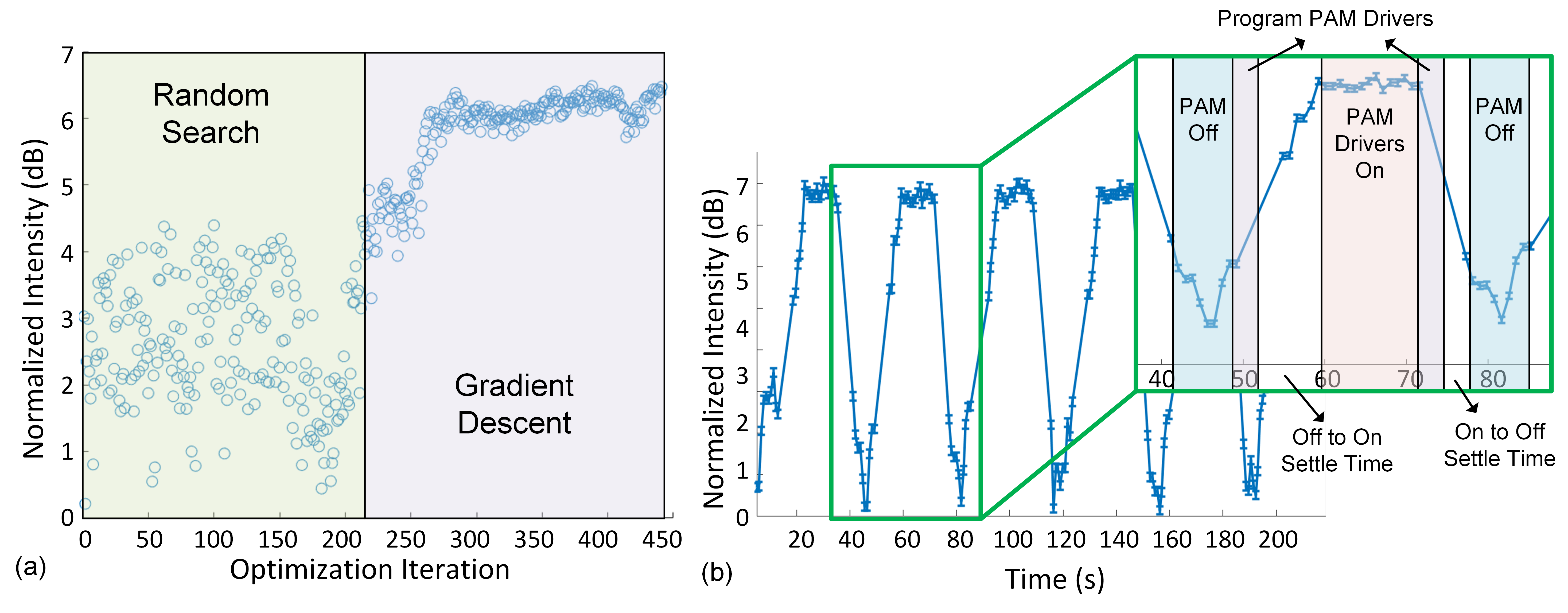
All of the phase and amplitude modulators in the array were optimized concurrently using the PAM drivers. These PAM drivers switch between different values with 10-bit resolution for the different columns. The large number of driver settings creates a very large search space for finding the optimized beam. In order to address this problem, we first performed a randomized optimization and recorded the broadside beam power value. After iterations, the randomized search found a PAM setting with increased signal power in the main beam. Afterward, a modified gradient search continues to optimize the main beam power from the best random-optimized beam. After iterations, gradient descent improves the beam by another . The optimization progression is shown in Fig. 7(a).
To verify the dynamic beamforming stability and repeatability of this OPA, we switched between the setting with all PAM drivers off and the optimum PAM setting for the broadside and recorded the dynamic changes in the normalized main beam power (with respect to the power coupled into the chip) as a function of time. The dynamic stability of the PAM drive is shown in Fig. 7(b). It takes seconds to program the PAM drivers. The thermal gradient variations on the chip settle in approximating seconds. The PAM drivers are able to consistently program the phase and amplitude modulators through the row-column drive scheme with less than ripple in the peak power.
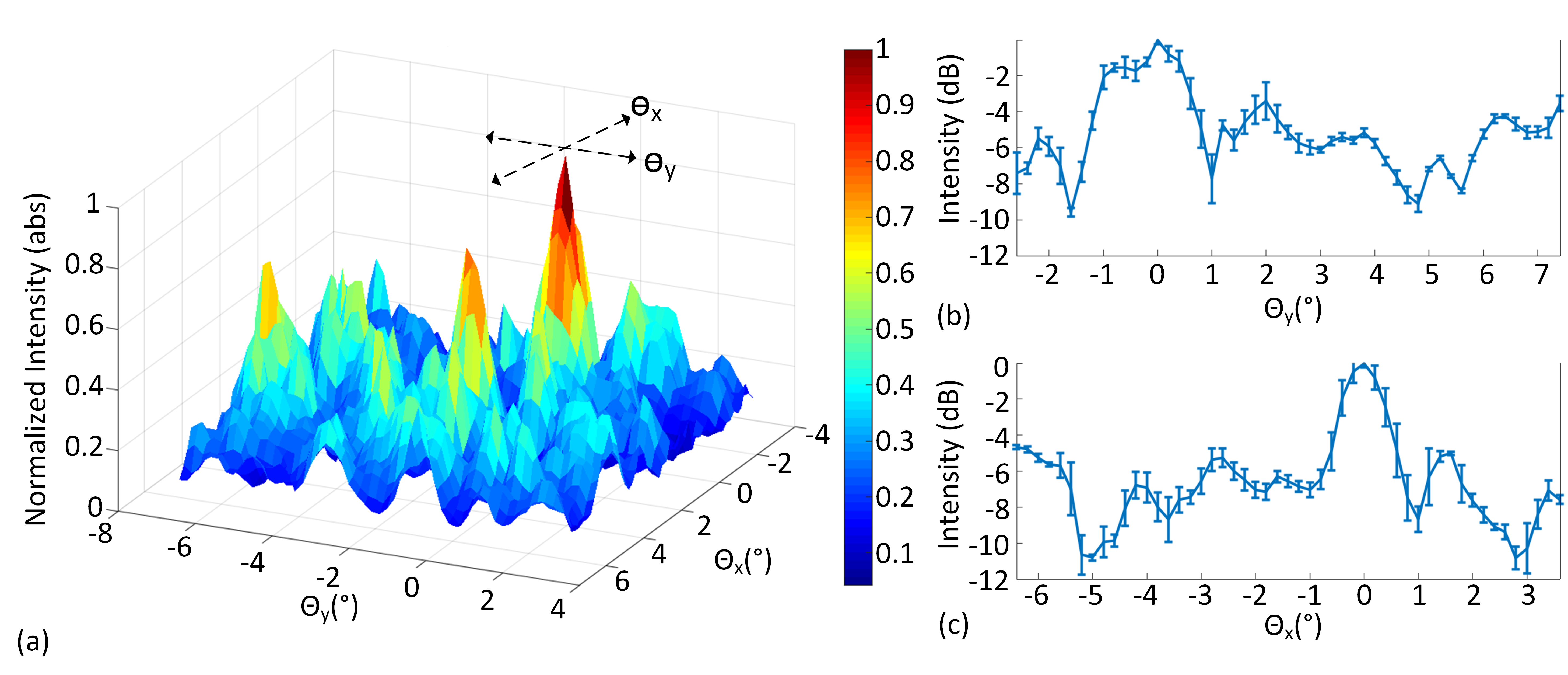
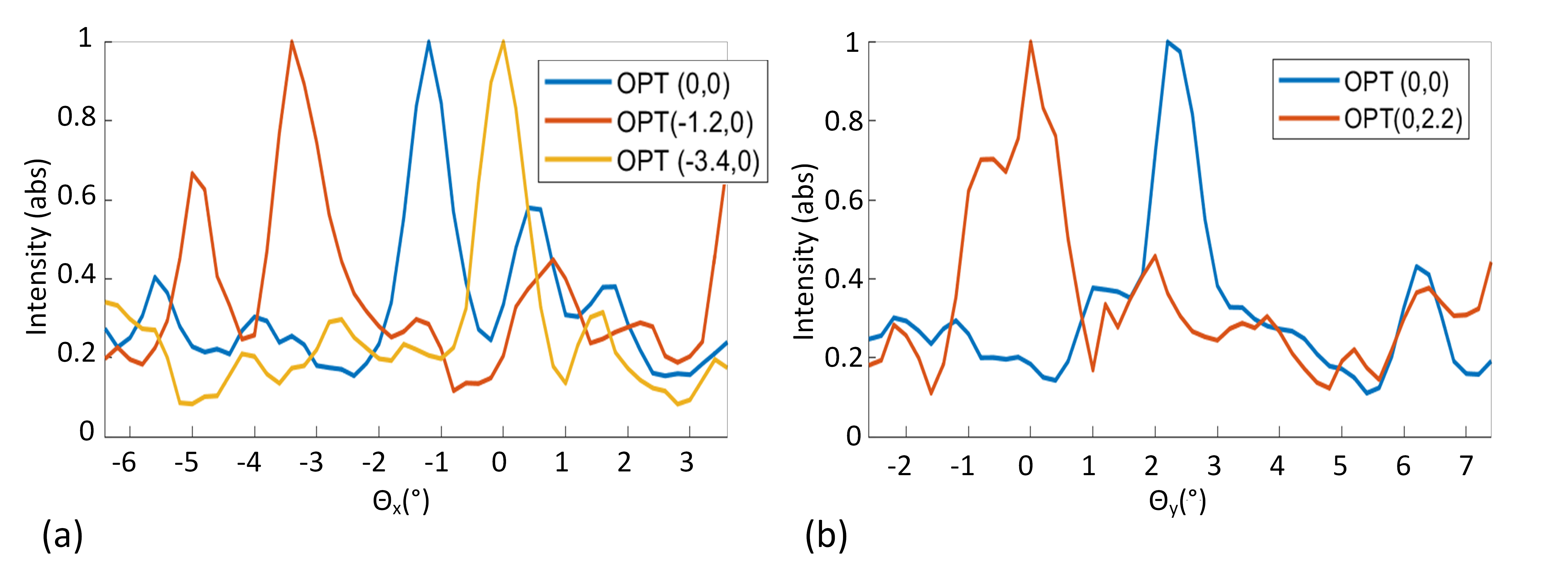
Afterward, we measured the optimized beam pattern using the aforementioned optical far-field measurement setup. The InGaAs photodector was rotated along the arc in directions at a 5cm distance. A 2D scan of the optimized beam pattern for the broadside direction in Fig. 8(a) shows no grating lobes in the measurement FOV of limited by the measurement setup. This measurement result was repeated three times and the cross-sectional view of the normalized broadside beam pattern with standard deviation for and are shown in Fig. 8(b) and (c) respectively. The optimization method used here was able to reduce the SLL to . Finally, we demonstrated the beam steering capability of this annular-ring aperture by optimizing the beam in several other directions. The InGaAs detector was positioned at and to demonstrate beam steering in direction and it was also positioned at to demonstrate beam steering in direction. The cross-sectional views of these steered beams are shown in Fig. 9.
5 Conclusion
In this work, we analyzed the advantages and design trade-offs of fixed linear density multi-annular-ring-aperture OPAs. Such OPAs reduce the sparse array design complexity due to their symmetric nature and permit signal distribution in a planar photonics process. Furthermore, the linear density of the elements in the OPA maintains a constant power efficiency for larger apertures reducing the beamwidth and the SLL. In a standard photonics process, we implemented an annular-ring aperture with 255 radiating elements and 510 phase and amplitude modulators. The proposed design uses a row-column drive, which reduces the electrical interconnect complexity from to . Furthermore, we measured the row-column drive programming reliability to be better than . Finally, we measured the far-field radiation pattern of the aperture for several directions, demonstrating the beamforming and beam steering capability for this aperture.
Acknowledgments
The authors would like to acknowledge Behrooz Abiri and Parham Porsandeh Khial for their valuable inputs in the design and analysis of this work.
Disclosures
The authors disclose no conflict of interest.
References
- [1] A. Tuantranont, V. Bright, J. Zhang, W. Zhang, J. Neff, and Y. Lee, “Optical beam steering using mems-controllable microlens array,” \JournalTitleSensors and Actuators A: Physical 91, 363–372 (2001). Proceedings of the Technical Digest of the 2000 Solid-State Sensors and Actuators Workshop.
- [2] Y. Wang, G. Zhou, X. Zhang, K. Kwon, P.-A. Blanche, N. Triesault, K. sik Yu, and M. C. Wu, “2d broadband beamsteering with large-scale mems optical phased array,” \JournalTitleOptica 6, 557–562 (2019).
- [3] F. Aflatouni, B. Abiri, A. Rekhi, and A. Hajimiri, “Nanophotonic coherent imager,” \JournalTitleOpt. Express 23, 5117–5125 (2015).
- [4] S. Chung, M. Nakai, S. Idres, Y. Ni, and H. Hashemi, “19.1 optical phased-array fmcw lidar with on-chip calibration,” in 2021 IEEE International Solid- State Circuits Conference (ISSCC), vol. 64 (2021), pp. 286–288.
- [5] F. Aflatouni, B. Abiri, A. Rekhi, and A. Hajimiri, “Nanophotonic projection system,” \JournalTitleOpt. Express 23, 21012–21022 (2015).
- [6] R. Fatemi, B. Abiri, and A. Hajimiri, “An 8×8 heterodyne lens-less opa camera,” in Conference on Lasers and Electro-Optics, (Optical Society of America, 2017), p. JW2A.9.
- [7] F. Ashtiani and F. Aflatouni, “Nxn optical phased array with 2n phase shifters,” \JournalTitleOpt. Express 27, 27183–27190 (2019).
- [8] M. S. Eggleston, F. Pardo, C. Bolle, B. Farah, N. Fontaine, H. Safar, M. Cappuzzo, C. Pollock, D. J. Bishop, and M. P. Earnshaw, “90db sensitivity in a chip-scale swept-source optical coherence tomography system,” in Conference on Lasers and Electro-Optics, (Optical Society of America, 2018), p. JTh5C.8.
- [9] A. White, P. Khial, F. Salehi, B. Hassibi, and A. Hajimiri, “A silicon photonics computational lensless active-flat-optics imaging system,” in Scientific Reports, (Nature, 2020), p. 1689.
- [10] C. V. Poulton, M. J. Byrd, P. Russo, E. Timurdogan, M. Khandaker, D. Vermeulen, and M. R. Watts, “Long-range lidar and free-space data communication with high-performance optical phased arrays,” \JournalTitleIEEE Journal of Selected Topics in Quantum Electronics 25, 1–8 (2019).
- [11] S. A. Miller, C. T. Phare, Y.-C. Chang, X. Ji, O. A. J. Gordillo, A. Mohanty, S. P. Roberts, M. C. Shin, B. Stern, M. Zadka, and M. Lipson, “512-element actively steered silicon phased array for low-power lidar,” in Conference on Lasers and Electro-Optics, (Optical Society of America, 2018), p. JTh5C.2.
- [12] J. Sun, E. Timurdogan, A. Yaacobi, E. S. Hosseini, and M. R. Watts, “Large-scale nanophotonic phased array,” \JournalTitleNature 493, 195–199 (2013).
- [13] S. Chung, H. Abediasl, and H. Hashemi, “15.4 a 1024-element scalable optical phased array in 0.18µm soi cmos,” in 2017 IEEE International Solid-State Circuits Conference (ISSCC), (2017), pp. 262–263.
- [14] N. Dostart, B. Zhang, A. Khilo, M. Brand, K. A. Qubaisi, D. Onural, D. Feldkhun, K. H. Wagner, and M. A. Popović, “Serpentine optical phased arrays for scalable integrated photonic lidar beam steering,” \JournalTitleOptica 7, 726–733 (2020).
- [15] C. V. Poulton, M. J. Byrd, M. Raval, Z. Su, N. Li, E. Timurdogan, D. Coolbaugh, D. Vermeulen, and M. R. Watts, “Large-scale silicon nitride nanophotonic phased arrays at infrared and visible wavelengths,” \JournalTitleOpt. Lett. 42, 21–24 (2017).
- [16] C. V. Poulton, M. J. Byrd, P. Russo, E. Timurdogan, M. Khandaker, D. Vermeulen, and M. R. Watts, “Long-range lidar and free-space data communication with high-performance optical phased arrays,” \JournalTitleIEEE Journal of Selected Topics in Quantum Electronics 25, 1–8 (2019).
- [17] W. Ma, S. Tan, K. Wang, W. Guo, Y. Liu, L. Liao, L. Zhou, J. Zhou, X. Li, L. Liang, and W. Li, “Practical two-dimensional beam steering system using an integrated tunable laser and an optical phased array,” \JournalTitleAppl. Opt. 59, 9985–9994 (2020).
- [18] D. O’Neill, “Element placement in thinned arrays using genetic algorithms,” in Proceedings of OCEANS’94, vol. 2 (1994), pp. II/301–II/306 vol.2.
- [19] R. Haupt, “Thinned arrays using genetic algorithms,” \JournalTitleIEEE Transactions on Antennas and Propagation 42, 993–999 (1994).
- [20] C. Balanis, Antenna Theory: Analysis and Design (Wiley, 2015).
- [21] M. E. Bialkowski and N. C. Karmakar, “A two-ring circular phased-array antenna for mobile satellite communications,” \JournalTitleIEEE Antennas and Propagation Magazine 41, 14–23 (1999).
- [22] F. Zhang, D. Zhang, and S. Pan, “Fast and wide-range optical beam steering with ultralow side lobes by applying an optimized multi-circular optical phased array,” \JournalTitleAppl. Opt. 57, 4977–4984 (2018).
- [23] N. H. Noordin, V. Zuniga, A. O. El-Rayis, N. Haridas, A. T. Erdogan, and T. Arslan, “Uniform circular arrays for phased array antenna,” in 2011 Loughborough Antennas Propagation Conference, (2011), pp. 1–4.
- [24] M. M. Khodier and M. Al-Aqeel, “Linear and circular array optimization: A study using particle swarm intelligence,” \JournalTitleProgress In Electromagnetics Research 15, 347–373 (2009).
- [25] A. Austeng and S. Holm, “Sparse 2-d arrays for 3-d phased array imaging-design methods,” \JournalTitleIEEE transactions on ultrasonics, ferroelectrics, and frequency control 49, 1073–1086 (2002).
- [26] P. Ioannides and C. Balanis, “Uniform circular arrays for smart antennas,” \JournalTitleIEEE Antennas and Propagation Magazine 47, 192–206 (2005).
- [27] R. Fatemi, A. Khachaturian, and A. Hajimiri, “A nonuniform sparse 2-d large-fov optical phased array with a low-power pwm drive,” \JournalTitleIEEE Journal of Solid-State Circuits 54, 1200–1215 (2019).
- [28] H. Abediasl and H. Hashemi, “Monolithic optical phased-array transceiver in a standard soi cmos process,” \JournalTitleOpt. Express 23, 6509–6519 (2015).