Predicting space-charge affected field emission current from curved tips
Abstract
Field emission studies incorporating the effect of space charge reveal that for planar emitters, the steady-state field , after initial transients, settles down to a value lower than the vacuum field . The ratio is a measure of the severity of space charge effect with being most severe and denoting the lack of significant effect. While, can be determined from a single numerical evaluation of the Laplace equation, is largely an unknown quantity whose value can be approximately found using physical models or can be determined ‘exactly’ by particle-in-cell or molecular dynamics codes. We propose here a simple model that applies to planar as well as curved emitters based on an application of Gauss’s law. The model is then refined using simple approximations for the magnitude of the anode field and the spread of the beam when it reaches the anode. The predictions are compared with existing molecular dynamics results for the planar case and particle-in-cell simulation results using PASUPAT for curved emitters. In both cases, the agreement is good. The method may also be applied to large area field emitters if the individual enhancement factors are known, for instance, using the hybrid model (D.Biswas, J. Vac. Sci. Technol. B 38, 063201 (2020)).
I The space charge affected current
I.1 Introduction
Field emission refers to the process by which electrons tunnel out from the surface of a conductor on application of a strong electric fieldFN ; Nordheim ; MG ; forbes2006 . The height and width of the tunneling potential barrier depends on the strength of the electric field. As a consequence, the field-emission current depends sensitively on the local electric field on the emitter surface with a small change in field resulting in a large change in emitted current.
The presence of field-emission electrons in a diode can itself be a cause for change in the local field on the emitter surfacestern29 ; ivey49 ; barbour53 ; vanVeen ; jensen97a ; jensen97b ; forbes2008 . If the applied macroscopic field is large enough to cause sufficient electron emission, the negative charge cloud lowers the magnitude of the local field on the emitter surface, thereby leading to a decrease in the field emission current. It may also happen that the local field becomes zero and emission stops altogether until the space charge moves away from the cathode and is eventually lost from the diode. Thus, the field emission current in a diode can be oscillatory initially till the local field at the emitter surface saturates with time and a steady-state prevails feng2006 ; jensen2015 ; torfason2015 .
Attempts to determinestern29 ; ivey49 ; barbour53 ; forbes2008 the steady-state cathode electric field and the emission current density for planar emitters have been made since the basic formulation of field emission by Fowler and NordheimFN (FN) in 1928 and subsequent corrections and approximations to the expression for the field emission current density for conductors MG ; forbes2006 . The connection between space charge and the current density is established by expressing the charge density where is the steady-state current density and the speedpuri2004 . The speed can be further expressed in terms of the potential using energy conservation. Thus, the Poisson equation can be expressed in 1-dimension as
| (1) |
where where and refer to the mass and charge of the electron. Assuming to be constant in a parallel-plate diode, Eq. (1) can be solved with at (grounded cathode) and at the anode placed at to get a relationbarbour53 ; forbes2008 between the steady-state field at the cathode and the current density :
| (2) |
This has to be solved self-consistently with a suitablesuitable ; forbes2007 ; forbes2008b ; DB_RR field emission equation in order to determine the space-charge affected field emission current density in terms of the applied voltage . It predicts for instance a saturation-like behaviour in the current density when used with the Murphy-GoodMG field emission expression for the current density. In an FN-plot, this gets manifested as a deviation from a straight line at high cathode fields.
I.2 space-charge affected current in the planar case
In a planar situation therefore, space charge does affect the field emission current. If we denote the electrostatic field in the absence of any charge by and the saturated field (after field emission has continued for a few transit times) by , a possible measurealternate ; db_scl of the severity of space charge effect may be taken to be the field reduction factorforbes2008 , . The subscript and refer to the Laplace and Poisson equations respectively forbes2008 . Clearly with denoting the lack of significant space charge effect and being the classical space charge limit child ; langmuir ; langmuir23 ; db_scl where and where is the Child-Langmuir current.
The dependence of the space-charge affected current on the field reduction factor can be simplified by re-writing Eq. (2) in terms of the dimensionless quantity where . The normalization of in effect is with respect to the planar Child-Langmuir current and at the space charge limit , assumes the value . Thus, Eq. (2) reduces to
| (3) |
which can be further simplified to yield
| (4) |
When , or , while corresponds to .
I.3 Extension of existing theory for curved emitters
It is difficult to extend the relation directly to the case of curved emitters since is no longer uniform. However, a plausible phenomenological relation may be arrived at by recalling a recent result on the space charge limited current for axially symmetric curved emitters. It states that the space charge limited current where is the radius of the base of the emitter and is the apex field enhancement factor (a constant)db_universal . Thus, it is natural to define the scaled field and current density as
| (5) | |||||
| (6) | |||||
| (7) |
where is the net space-charge affected emitter current and is a factor that is hitherto unknown. A plausible relation between the space-charge affected current and apex field can thus be obtained by substituting and in Eq. (4) so that
| (8) |
Eq. (8) has the correct limiting behaviour for an axially symmetric curved emitter mounted in a parallel plate diode configuration. The weak space charge regime has the solution
| (9) |
which can be equivalently expressed as
| (10) |
with as a fitting parameter and evaluated with as defined in Eq. (7). The linear behaviour predicted by Eq. (10) has recently been observed in a PIC simulationrk2021 where the normalized current density was defined as with taking values between 0.5 and 1. In the ( plane, Eq. (10) is expressed as
| (11) |
so that the slope of the line is . For the case , the slope is thus while the reported valuerk2021 was -0.073. Thus, .
While Eq. (8) together with Eqns. (5-7) constitute a major step in dealing with axially symmetric curved emitters, it is nevertheless an ad-hoc extension of the planar model. The free parameter is a reflection of this approach. Alternately, if is set to unity, the factor which defines the average current density must be obtained from a fit to numerical results. There is thus sufficient scope and motivation to build an alternate formalism which suits both curved emitters and planar emitters with a finite active area.
I.4 Scope for an alternate model
A variety of alternate approaches have also been used to study space charge effects on field emission jensen97a ; jensen97b ; lin2007 ; rokhlenko2010 ; jensen2010 ; rokhlenko2013 ; jensen2014 ; jensen2015 . Some of these, based on transit time, are able to reproduce features of the time variation of the cathode field and the steady-state that follows, especially for planar emitters.
The field reduction factor , which is a measure of space charge severity, may depend on several factors for a planar emitting patch or a curved emitter apex. In a molecular dynamics simulationtorfason2015 , it was found that keeping other features of a parallel plate diode invariant and varying only the size of the planar emitting patch, the value of decreases as the size of the patch is increased. Thus, two emitters with emitting areas and () but having the same and transit time , will be affected by space charge differently with the smaller one being relatively less affected torfason2015 . The severity of space charge may also depend on the transit time , the vacuum field and several other factors. For an axially symmetric curved emitters, there are very few studies torfason2016 ; rk2021 . The dependence of on the transit time and the vacuum field are expected to persist for curved emitters.
The present communication deals with a semi-analytical model, one that naturally accommodates curved emitters and can provide the time variation of the apex field and emitted current and estimates of and without much computational effort. It aims to predict some of the results reported earlier. While it is not intended as a substitute for PIC methods, it can be used as a design tool to scan the parameter space since a full 3-dimensional PIC modelling may be extremely time consuming and expensive.
We shall first outline the model in section II and state the various approximations that may be used to improve the prediction. This will be followed by a comparison with a published MD simulation for planar geometry and our own PIC simulations using PASUPATdb_scl ; db_multiscale ; rk2021 .
II The semi-analytical model
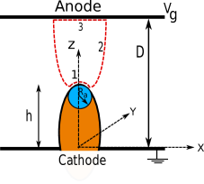
Consider an axially symmetric curved emitter of height and apex radius of curvature as shown in Fig. 1. It is mounted on the grounded cathode in a parallel plate diode configuration with the plate separation , and the anode at a potential . The macroscopic (applied) field is thus while the local field at the apex of the curved emitter is prior to the emission of electrons. Emission can occur from any point on the curved surface (defined by ) depending on the strength of the local field at a point () on the surface.
After emission begins (), the space between the plates has an amount of charge while the local field at the apex is . Since the field emission current densityMG ; forbes2006 depends on the local field , the emitted current can vary with time. For , where is the ballistic transit time, where
| (12) | |||||
| (13) |
where denotes the surface of the curved emitter and the field emission current density
| (14) |
with
| (15) | |||||
| (16) | |||||
| (17) |
where , are the conventional Fowler-Nordheim constants, is the Schottky constant with and is the work function of the material under consideration in eV. If the apex radius of curvature is smaller than nm, it is advisable to use the curvature-corrected form of the field emission current densityDB_RR ; db_rr_2021 .
Note that depends on time when emission is space charge affected and so is the current density . In general, it suffices to take the limits of integration as . For , electrons leave the diode region so that can decrease leading to an increase in . The loss of electrons can be approximately modelled as
| (18) |
so that the electrons emitted at arrive at the anode at time . In the above is the Heaviside step function which is zero for and equals 1 for . Thus, at any time , the amount of charge in the diode is
| (19) |
An oscillatory behaviour in is thus to be expected, especially if the field at the emitter apex falls substantially from its vacuum value leading to periods of low current injection.
Note that the local field at any point () close to the apex, is related to through the generalized cosine lawcosine1 ; cosine2
| (20) |
which has been found to hold for emitters with parabolic endcaps obeying . This local variation holds in the absence of space charge as shown analytically (using the nonlinear line charge model) as well as numerically. It has recently been demonstrated that the cosine variation holds for moderate space charge intensity with reasonable accuracyrk2021 .
A relation between and can be obtained by applying Gauss’s law twice, first at and then at some arbitrary time . Consider a Gaussian surface denoted by the dashed closed curve marked 1,2,3 in Fig. 1. At time , the field close to the anode (surface 3) is while close to the emitter-apex (on surface 1), the field is . Elsewhere on surface 1, the magnitude of the electric field is assumed to vary accordingly to the generalized cosine law so that the total flux passing through surface 1 may be evaluated.
If we further choose surface 2 such that the field lines lie on it (rather than intersecting it any point), the flux through surface 2 is zero. Also, since there is no charge present at time ,
| (21) |
which implies . The flux through the parabolic surface 1 may be evaluated as follows:
| (22) | |||||
where and . For a sharp emitter where , the flux is . In general, and since at ,
| (23) |
Thus for a curved emitter, the flux tube expands on reaching the anode.
We can now consider the case when the Gaussian surface encloses an amount of charge and apply Gauss’s law again. If we assume the generalized cosine law to be approximately valid in the presence of space charge,
| (24) |
where has been replaced by . Surface 2 can again be chosen such that field lines do not cross it and hence . Finally, we recognize the fact that surface 3 (infinitesimally close to the anode) may be larger on account of space charge and the field may be significantly larger in magnitude than . We shall denote the area and anode field by and respectively and their asymptotic steady-state values by and .
The unknown quantities are thus (i) which is the field at the apex of the curved emitter (ii) which is the field at the flat anode (iii) which is the area through which is the anodic-flux reaches the curved emitter tip from the apex to . While and are required to refine the calculation of , we can assume as a first approximation that they assume their vacuum values i.e. while .
With this first approximation, an application of Gauss’s law leads us to the equation
| (25) |
| (26) |
where and the effective area at the curved emitter
| (27) |
Since depends on the field , Eq. (26) can be differentiated to yield
| (28) |
It is clear that the injection of charges into the diode and their subsequent loss at the anode leads to an oscillatory evolution of the apex field if emission falls substantially from the initial values.
II.1 The anode field approximation
In order to improve the predictive power of the model, it is important to approximate the anode field . At , when the field at the emitter is , the anode field is . We are also aware from planar space charge limited flows that when the field at the cathode is zero (the limiting case), the anode field assumes the value . A simple linear interpolation between these two points and on the plane, gives us the relation
| (29) |
Since varies with time, the dependence on time is explicitly shown. Note that Eq. (29) reproduces the two limits since and the anode field assumes the value when .
If we consider the anode area to be invariant in time and assume its vacuum value, an application of Gauss’s law with only the anode-field correction leads us to the equation
| (30) |
so that on rearranging terms
| (31) |
and differentiating, we have
| (32) |
Thus, the anode-field correction introduces a factor in the rate at which the apex field changes.
II.2 The anode area approximation
At the next level, we can also introduce an anode area approximation using the parallel-plate diode as a guide. Before emission starts, the flux tube maps equal area at the cathode and anode in a planar diode while in case of a curved emitter, the flux tube maps an area of the cathode that is times more at the anode (see Eq. 23). Thus, when the field at the emitter apex is , the area at anode is .
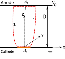
The planar Child-Langmuir law can again be used to obtain a second point. Numerical and analytical results show that if the emitting patch is finite, the Child-Langmuir current density can be expressed as where represents the size of the emitting patch and is a constant that depends on the shape of the patch. Thus, for a circular patch, while is its radius. The relevance of the factor in the planar case with finite emission area (see Fig. 2) can be understood by considering the Gaussian surface as a the flux tube extending from the cathode having an area , to the anode having an area . On applying Gauss’s law and assuming that the cathode field is zero, we have where . Assuming and where the average speed as in the infinite parallel plate case, it follows that . In other words, the area of the emitting patch at the cathode is mapped to a patch at the anode that is larger by a factor . When applied to a curved emitter having an effective emitting area , the area at the anode is when the field at the apex is zero.
A linear interpolation between these two points gives
| (33) |
Note that Eq. (33) states that at when , while when , . For an axially symmetric curved emitter, may be taken to be and .
An application of Gauss’s law with both the anode field and area corrections leads to the equation
| (34) |
which can be rearranged and differentiated to yield
| (35) |
where
| (36) |
Eq. (28), Eq. (32) and (35) along with Eq. (36) provide successively better approximations for determining the steady state electric field at the emitter apex. Note that the value of is not known with any accuracy and may need to be determined by fitting Particle-in-Cell or Molecular Dynamics data, especially for curved emitters. Nevertheless, it is expected to provide a fast approximate determination of the space charge affected field emission current.
The model presented here is also applicable to a cluster of emitters or a large area field emitter (LAFE). The hybrid model proposed recentlydb_rudra1 ; rudra_db ; db_rudra2 ; anodeprox ; db_hybrid can be used to determine the apex field enhancement factor of individual emitters in the LAFE before emission starts, and so long as two emitters are not too close to each other for mutual space charge effects to kick in, the formalism presented here can be used for each emitter.
III Numerical Results
We shall use Eq. (35) along with Eq. (36), Eq. (13) and Eq. (14) to test the usefulness of the theoretical model proposed in Section II. While, we expect the gross features of the time evolution to be visible, finer details are not expected since they are beyond the scope of the approximations used. It would be interesting to see if the steady state field is determined consistently with reasonable accuracy.
III.1 Comparison with planar result
A first test of the model is the extensive Molecular Dynamics (MD) data reported in Ref. [torfason2015, ] for a square emitting patch of side length in a planar diode geometry. The gap between the anode and cathode plates is nm, the potential difference kV while varies from nm to nm. The emission current density follows Eq. (14) with a work function eV. Since the emitting area is a flat square, refers to the field on the emitter surface. The vacuum field is thus V/nm. When emission starts, it is assumed that the field on the emitter is independent of the location on the patch resulting in uniform emission (in reality, the wings have larger current density especially when is small). Thus where is computed using Eq. (14).
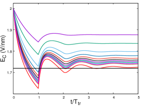
When the patch length is large (), the results are expected to mimic the 1-D PIC result reported in Ref. [feng2006, ] where the space-charge affected cathode field is around V/nm. The MD simulationtorfason2015 indeed approaches this value when nm. For the model presented here, the anode-area correction is expected to be small for nm and the results should not be very sensitive on the value of . This is indeed found to true with very little variation as varies from nearly 0 to 1. The smaller values are however poorly reproduced for standard values of in the range with being the value appropriate for a square of side-length . Fig. (3) shows a plot of the cathode field variation for for values of nm (bottom to top curves). While these do not match perfectly with the MD simulation results (see Fig. 4 of Ref. [torfason2015, ]) especially for nm, the trend is very nearly the same and the error is reasonably small.
III.2 Curved emitters
Planar field emitters require high macroscopic fields in the V/nm range due to the lack of field enhancement (). In practice, field emission occurs from specially designed curved emitters or nano-protrusions on a smooth surface since they require a much smaller macroscopic field. These are thus the natural geometries that need to be investigated for the effect of space charge on field emission.
We shall consider here an axially symmetric curved emitter for which the projected emission area can be considered to be circular of radius and the free parameter can be chosen to be equal to . The hemi-ellipsoid is an example of such a geometry. While, the Laplacian problem for the hemi-ellipsoid placed on a conducting plane with the anode far away can be solved analytically smythe ; kosmahl , the presence of space charge makes the problem non-trivial and requires numerical investigation. In order to test our model, we shall consider various magnifications of the basic hemi-ellipsoidal emitter having a height m and base radius m. The apex radius of curvature m. The spacing between the anode and cathode plates is m. The work function is considered to be eV.
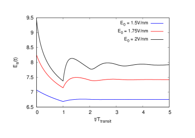
The predictions of the model for and kV corresponding to and V/nm are shown in Fig. 4. While space charge affects the apex field at all three values of the macroscopic field, it is strong enough to causes oscillations at and V/nm. The nature of oscillations is similar to the planar case with the period linked to the transit time as observed in planar molecular dynamics simulationstorfason2015 and theoretical modelsjensen2015 . Planar PIC simulations also display oscillationsfeng2006 but these have not been observed yet in 3-D simulations using curved emitters edelen2020 which are considerably more resource intensive.
We shall henceforth compare the model predictions with PIC simulations performed using PASUPAT db_scl ; db_multiscale ; rk2021 with a field emission module based on the cosine law db_parabolic ; db_multiscale ; rk2021 . Our focus will be on the steady state values of the apex field and emitted current and these will be compared with the predictions of the model for various geometric diode parameters. In the PIC simulation using PASUPAT, the hemiellipsoid and cathode plate are considered to be grounded perfect electrical conductors (PECs) while the anode is a PEC at a voltage . The centre of the hemiellipsoid is at while the transverse boundaries are located at m and have Neumann boundary condition imposed on them. Since the height of the emitter is small compared to the extent of the boundary in the and directions, it is close to being an isolated emitter. The value of as calculated using PASUPAT is 4.715 which coincides with the value evaluated using COMSOL. The apex field enhancement effect for an isolated emitter is around . Thus, there is a mild shielding effect due to the computational boundary not being very far away.
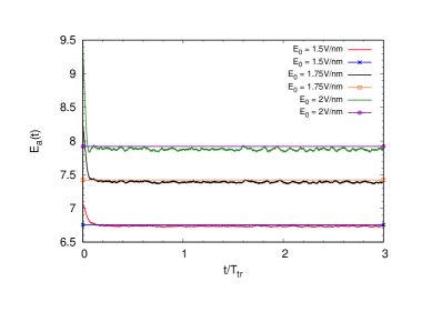
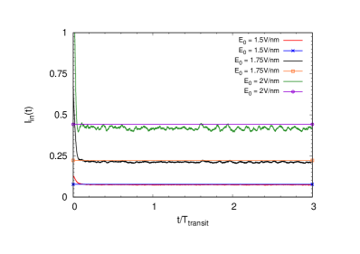
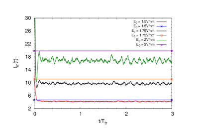
For the diode described above with m, the PIC results for and V/nm are shown in Fig. 5. The straight line in each case marks the prediction of the model presented in section II for the steady-state apex field. The corresponding result for the emission current is shown in Fig. 6. The agreement is reasonably good especially at the lower values of the macroscopic field where the agreement with the cosine law is goodrk2021 . Note that in order to keep the fluctuations small, the number of time steps per transit time ( has been kept identical for all the simulations.
We shall next consider the effect of transit time by scaling the size of the diode while keeping the field at the apex as invariant. We shall first consider a scaling down of all geometric quantities by a factor of 10. Thus, m, m m and the transverse computational boundaries are at m. In terms of , the transit time . Since the enhancement factor is unchanged by the scaling, remains the same if is maintained at the previous values. Thus . Thus, on scaling down the diode by a factor of 10, the transit time decreases by a factor of resulting in faster loss of charges from the diode. The effect of space charge is thus expected to be weaker. The PIC simulation results for the scaled down diode are shown in Fig. 7 and Fig. 8. A comparison with Fig. 5 shows the drop in field from the vacuum values to be much smaller indicating a larger value of . Note that the agreement with the cosine law in the presence of space charge is excellent for this scaled-down dioderk2021 .
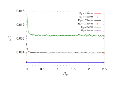
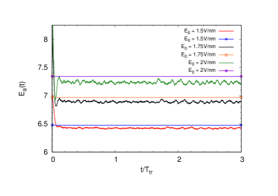
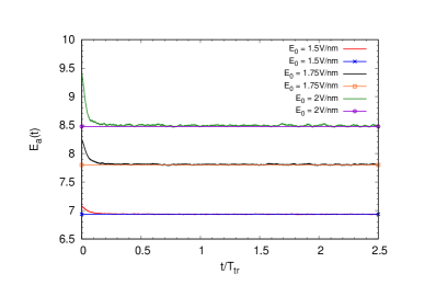
We next consider a scaled-up diode to check for the consistency of our results. The scaling factor is 10 so that m, m m and the transverse computational boundaries are at m. The results for the time variation of the apex field and injected current are shown in Figs. 9 and 10. The effect of space charge is much stronger as compared to the unscaled case (m) thus establishing the importance of transit time in determining the severity of space charge effect on field emission. Not surprisingly, even at V/nm, the agreement between the model and the PIC result is not perfect. This coincides with the larger deviation from the cosine law for the scaled-up dioderk2021 .
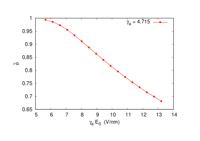
It is clear from these results that the model is able to predict the steady-state space-charge affected apex field and the injected current reasonably well, when the space-charge effect is moderate. We can use the values obtained from the model to quantify the severity of space-charge. Fig. 11 shows a plot of as a function of for the model considered where m and the apex enhancement factor is . Note that the upper limit of the vacuum field used in the Fig. 11 and 13 is V/nm. This is to ensure that the top of the potential barrier remains above the Fermi level. The values of for exceeding 10V/nm or are not very accurate due to larger deviations from the cosine law. They are however expected to be indicative of the general trend.
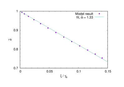
The model results can also be cast in a () plot for completeness. This is shown in Fig. 12 for m. Also shown is the straight line of Eq. (10) with the parameter , obtained by a least square fit.
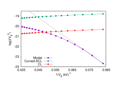
Finally, the data obtained using the space-charge affected field emission model is shown as an FN plot in Fig. 13. Clearly, the space charge affected field emission current deviates from the straight line as observed earlier barbour53 ; jensen97a ; jensen97b ; forbes2008 . Also shown alongside are FN plots of 2 different space charge limited currents. The first of these (solid triangles in Fig. 13) is the planar Child-Langmuir current from an area equal to the base of the curved emitter. Thus, where
| (37) |
is the space charge limited current from a planar surface. The second (solid circles in Fig. 13) uses the recently reported approximate space charge limited current for curved emitters
| (38) |
which reduces to the planar case for .
The space-charge affected field emission current can thus exceed the planar space charge limit but is bounded by the space charge limited current for a curved emitter.
IV Discussions
We have put forward a time-dependent model for space-charge affected field emission that is simple to implement and takes only a few seconds to yield the time evolution of the apex field and emitted current over several transit times. The steady state values achieved were compared with the PIC code PASUPAT and found to be in good agreement keeping the only free parameter fixed at which corresponds to emission from a circular patch. The agreement was excellent under low and moderate space-charge conditions corresponding to smaller transit times or lower vacuum fields, for which the agreement with the cosine law of field variation is good.
The model is also applicable to a cluster of emitters or a large area field emitter (LAFE) arranged randomly or in an ordered fashion so long as the individual field enhancement factors are knowndb_rudra1 ; rudra_db ; db_rudra2 ; anodeprox ; db_hybrid and two emitters are not too close to each other for mutual space charge effects to kick in. In the example chosen to verify the model is that of emitters on an infinite square lattice with Neumann boundary condition on the transverse computational boundaries placed at half the lattice constant. The effect of other emitters is manifested in the slightly lower field enhancement factor due to the shielding effect. In general, if is large enough (), the hybrid modeldb_rudra2 ; db_hybrid can be used to calculate the field enhancement factor of individual emitters in a LAFE and hence the net space-charge affected field emission current may be calculated.
V Acknowledgements
PASUPAT simulations were performed on ANUPAM-AGANYA super-computing facility at Computer Division, BARC.
VI Author Declarations
VI.1 Conflict of interest
The authors have no conflicts to disclose.
VI.2 Data Availability
The data that supports the findings of this study are available within the article.
Data Availability: The data that supports the findings of this study are available within the article.
VII References
References
- (1) R. H. Fowler and L. W. Nordheim, Proc. Roy. Soc. Ser. A 119, 173 (1928).
- (2) L. W. Nordheim, Proc. R. Soc. London, Ser. A 121, 626 (1928).
- (3) E. L. Murphy and R. H. Good, Phys. Rev. 102, 1464 (1956).
- (4) R. G. Forbes, Appl. Phys. Lett. 89, 113122 (2006).
- (5) T. E. Stern, B. S. Gossling, and R. H. Fowler, Proc. R. Soc. London, Ser. A
- (6) H. F. Ivey, Phys. Rev. 76, 554 (1949).
- (7) J. P. Barbour, W. W. Dolan, J. K. Trolan, E. E. Martin, and W. P. Dyke, Phys. Rev. 92, 45 (1953).
- (8) G. N. A. van Veen, J. Vac. ScI. Technol. B 12, 655 (1994).
- (9) K. L. Jensen, P. Mukhopadhyay-Phillips, E. G. Zaidman, K. Nguyen, M. A. Kodis, L. Malsawma, C. Hor,Applied Surface Science 111 (1997) 204.
- (10) K. L. Jensen, M. Kodis, R. Murphy, and E. G. Zaidman, J. Appl. Phys. 82, 845 (1997).
- (11) R. Forbes, J. Appl. Phys., 104, 084303 (2008).
- (12) Y. Feng and J. P. Verboncoeur, Phys. Plasmas, 13, 073105 (2006).
- (13) K. L. Jensen, D. A. Shiffler, I. M. Rittersdorf, J. L. Lebowitz, J. R. Harris, Y. Y. Lau, J. J. Petillo, W. Tang, and J. W. Luginsland, J. Appl. Phys. 117, 194902 (2015).
- (14) K. Torfason, A. Valfells and A. Manolescu Phys. Plasmas 22, 033109 (2015).
- (15) R. R. Puri, D. Biswas and R. Kumar, Phys. Plasmas 11, 1178 (2004).
- (16) The standard field emission equation applicable to conductors is due to Murphy and GoodMG . Other variants of this exist. See for instance Forbes [forbes2007, ]. Depending on the curvature of the emitter, curvature-corrected field emission equations existDB_RR .
- (17) R. G. Forbes and J. H. B. Deane, Proc. R. Soc. A.463, 2907 (2007).
- (18) R. G. Forbes, J. Vac. Sci. Technol. B26, 788 (2008).
- (19) D. Biswas and R. Ramachandran, J. Vac. Sci. Technol. B37, 021801 (2019).
- (20) An alternate measure of space charge strength is the ratio of the steady-state field emission current and the space charge limited current. Note however that the SCL current depends linearly on the apex field enhancement factor db_scl .
- (21) G. Singh, R. Kumar and D. Biswas, Physics of Plasmas 27, 104501 (2020).
- (22) C. D. Child, Phys. Rev. 32, 492 (1911).
- (23) I. Langmuir, Phys. Rev. 2, 450 (1913).
- (24) I. Langmuir, Phys. Rev. 21, 419 (1923).
- (25) D. Biswas, Physics of Plasmas, 25, 043113 (2018).
- (26) R. Kumar, G. Singh and D. Biswas, ‘Approximate universality in the electric field variation on a field-emitter tip in the presence of space charge’, Physics of Plasmas (in press); https://arxiv.org/abs/2105.09839.
- (27) M.-C. Lin, J. Vac. Sci. Technol. B25, 493 (2007)
- (28) A. Rokhlenko, K. L. Jensen and J. L. Lebowitz, J. Appl. Phys. 107, 014904 (2010).
- (29) K. L. Jensen, J. Appl. Phys. 107, 014905 (2010)
- (30) A. Rokhlenko and J. L. Lebowitz, J. Appl. Phys. 114, 233302 (2013).
- (31) K. L. Jensen, D. A. Shiffler, J. J. Petillo, Z. Pan, and J. W. Luginsland, Phys. Rev. ST Accel. Beams 17, 043402 (2014).
- (32) K. Torfason, A. Valfells and A. Manolescu Phys. Plasmas 23, 123119 (2016).
- (33) S. G. Sarkar, R. Kumar, G. Singh and D. Biswas, Physics of Plasmas 28, 013111 (2021).
- (34) D. Biswas and R. Ramachandran, Journal of Applied Physics, 129, 194303 (2021).
- (35) D. Biswas, G. Singh, S. G. Sarkar and R. Kumar, Ultramicroscopy 185, 1 (2018)
- (36) D. Biswas, G. Singh and Rajasree R., Physica E, 109, 179 (2019).
- (37) W. R. Smythe, Static and dynamic electricity, ( Taylor and Francis, 1989).
- (38) H. G. Kosmahl, IEEE Trans. Electron Devices 38, 1534 (1991).
- (39) J. P. Edelen, N. M. Cook, C. G. Hall, Y. Hu, X. Tan and J-L. Vay, J. Vac. Sci. Technol. B 38, 043201 (2020).
- (40) D. Biswas, Physics of Plasmas 25, 043105 (2018).
- (41) D. Biswas and R. Rudra, Physics of Plasmas 25, 083105 (2018).
- (42) R. Rudra and D. Biswas, AIP Advances, 9, 125207 (2019).
- (43) D. Biswas and R. Rudra, J. Vac. Sci. Technol. B38, 023207 (2020).
- (44) D. Biswas, Physics of Plasmas, 26, 073106 (2019).
- (45) D. Biswas, J. Vac. Sci. Technol. B 38, 063201 (2020).