Bulk band structure of Sb2Te3 determined by angle-resolved photoemission spectroscopy
Abstract
The bulk band structure of the topological insulator Sb2Te3 is investigated by angle-resolved photoemission spectroscopy. Of particular interest is the dispersion of the uppermost valence band with respect to the topological surface state Dirac point. The valence band maximum has been calculated to be either near the Brillouin zone centre or in a low-symmetry position in the azimuthal direction. In order to observe the full energy range of the valence band, the strongly p-doped crystals are counter-doped by surface alkali adsorption. The data show that that the absolute valence band maximum is likely to be found at the bulk point and predictions of a low-symmetry position with an energy higher than the surface Dirac point can be ruled out.
I Introduction
Sb2Te3 was one of the first materials recognised as a three-dimensional topological insulator (TI) with a single Dirac cone surface state Zhang et al. (2009); Hsieh et al. (2009). Its electronic structure is very similar to both that of Bi2Se3 and Bi2Te3, materials that are viewed as prototypical for this family of TIs Ando (2013). An important point is that both Bi2Se3 and Bi2Te3 are plagued by degenerate n-doping due to common crystalline defects such that they are ill-suited for experimentally assessing or technologically exploiting transport through the surface states instead of the bulk states. Sb2Te3, on the other hand, is typically strongly p-doped due to the presence of substitutional Sb on Te sites Horák et al. (1988).
As a consequence of the p-doping, only the lower part of the surface state Dirac cone is accessible to angle-resolved photoemission spectroscopy (ARPES) experiments that are routinely used to characterise the predicted surface state dispersion of TIs Hasan and Kane (2010) but can only access filled states. This problem can be circumvented by strong surface doping via the adsorption of alkali metals Seibel et al. (2012) or by pumping of electrons into unoccupied states Reimann et al. (2014). The surface state dispersion can also be characterised by scanning tunnelling spectroscopy in the presence of a strong magnetic field, via the energy spacing of the resulting Landau levels Jiang et al. (2012a).
The existence of metallic surface states in TIs is enforced by a band inversion, i.e., a swapping of the -like valence band (VB) with the -like conduction band around a high symmetry point, leading to a “negative” band gap. More precisely, the relation of the parity invariants of the eight time-reversal invariant momenta in the bulk Brillouin zone Fu et al. (2007) dictates the position of the “negative” band gap and the Fermi contour topology of the surface states. For Sb2Te3 and most similar crystals, is -1 while it is 1 for all the other time-reversal invariant momenta, implying a negative band gap at the bulk point and that the surface point is encircled by a single non spin-degenerate surface Fermi contour.
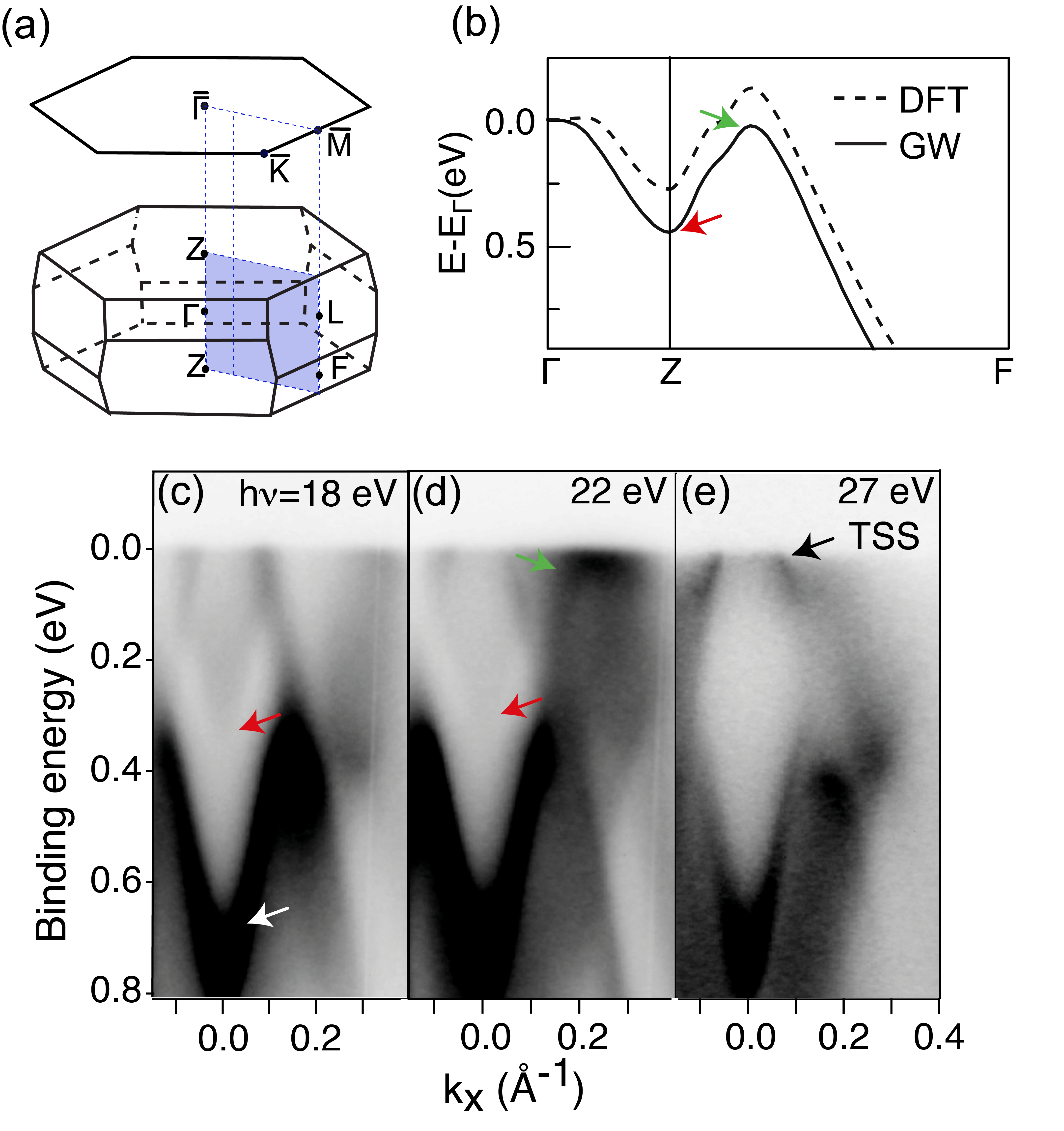
The negative band gap has a number of interesting consequences for the effect of many-body interactions on the overall electronic structure of the TIs. In a conventional (non-topological) semiconductor, many-body corrections as implemented in a GW calculation mostly serve to correct the well-known tendency of density functional theory (DFT) to underestimate the size of the band gap. This happens by an approximately rigid shift of VBs and conduction bands away from each other. In a TI, this rigid increase of the band gap still takes place in most of the Brillouin zone (BZ) but not in the region of the negative band gap Kioupakis et al. (2010); Yazyev et al. (2012); Nechaev and Chulkov (2013); Aguilera et al. (2013); Förster et al. (2016). This leads to a -dependent deformation of the bands which may result in wrong predictions about the band structure and topology Vidal et al. (2011). Sb2Te3 serves as an excellent example of this. DFT calculations along high-symmetry directions typically place the absolute valence band maximum (VBM) between the Z and F points of the BZ Zhang et al. (2010); Menshchikova et al. (2011), see Figure 1(a), (b). The inclusion of many-body corrections such as realised in the GW approximation changes this picture and places the absolute VBM at the bulk point Aguilera et al. (2013); Nechaev et al. (2015); Förster et al. (2016). Actually, merely displaying the band structure between Z and F may not even show the correct position of the VBM in the DFT calculations because the true VBM could be at any position in the plane given by the direction in the surface BZ Nechaev et al. (2015) (blue shaded plane in Figure 1(a)), so that the true VBM in DFT might be even higher than the one between Z and F. Note that the band structure differences are not small and can exceed 100 meV, a quarter of the total width of the highest VB along . A similar interplay between absolute VBM position and many-body corrections takes place in Bi2Se3 Nechaev et al. (2013) and Bi2Te3 Michiardi et al. (2014).
The question of where the absolute VBM is found is not only of interest as a benchmark for many-body corrections in band structure calculations, it also has important consequences for the TIs’ transport properties. In particular, the relative position of surface state Dirac point and bulk state dispersion restricts the range of energies in which surface state-dominated transport is achievable Barreto et al. (2014). In a DFT surface band structure calculation, the absolute VBM in the plane lies above the Dirac point of the topological surface state Hsieh et al. (2009); Menshchikova et al. (2011), implying that no level of doping would result in a situation where electronic transport could be dominated by the surface state electrons near the Dirac point. On the other hand, such surface-dominated transport is possible when the VBM in the direction lies below the surface state Dirac point.
Synchrotron radiation-based ARPES studies were able to map the relevant bulk band structure for Bi2Se3 Nechaev et al. (2013) and Bi2Te3 Michiardi et al. (2014), underlining the importance of the corrections in the GW calculations. However, the aforementioned p-doping makes the band structure determination of Sb2Te3 by ARPES more challenging because relevant states can be placed above the Fermi energy in a degenerately doped crystal. Several ARPES investigations from Sb2Te3 single crystal surfaces have been published Hsieh et al. (2009); Seibel et al. (2012); Pauly et al. (2012); Reimann et al. (2014); Seibel et al. (2015), as well as from thin films Wang et al. (2010); Plucinski et al. (2013) where the doping can be controlled by growth conditions Jiang et al. (2012b). The focus of most studies were the topological surface states. Here we study the dispersion of the topmost VB in order to determine the position and energy of the global VBM. We exploit variable photon energies to explore the complete plane. We gain access to the normally unoccupied states by doping the surface with alkali atoms. A similar approach has been used in Ref. Seibel et al. (2012) in order to access the surface state Dirac point by ARPES.
II Experimental Details
Sb2Te3 crystals were grown following the procedure outlined in Ref. Ruckhofer et al. (2021). Attempts were made to synthesize bulk crystals with a smaller p-doping or to achieve chemical bulk counter-doping but these were not successful. ARPES experiments were performed on the SGM-3 beamline of ASTRID2 in Aarhus Hoffmann et al. (2004). Samples were cleaved at room temperature in a pressure better than mbar, prior to the measurement at mbar. The sample temperature during ARPES measurements was 35 K. Energy and angular resolution were better than 50 meV and 0.1∘, respectively. Rb was dosed from a well-outgassed SAES Getters dispenser during the acquisition of photoemission data. As expected, Rb adsorption leads to a strong electrostatic doping effect but the adsorption on the Sb2Te3 surface is highly unstable. Stopping the Rb evaporation leads to an immediate loss of doping. The Rb coverage was estimated using core level spectroscopy. However, due to the unstable adsorption, this cannot be measured at the same time as the VB spectra but requires a separate cleave of the sample and the evaporation of Rb under the same conditions.
III Results and Discussion
We start out by presenting data from as-cleaved samples. Due to the p-doping of the material, the VBM at and the surface state Dirac point are above the Fermi energy and thus not accessible to ARPES. However, inspecting data from pristine surfaces – instead of alkali-doped samples – has the advantage of giving higher quality spectra and the data is thus useful for identifying the salient features and their approximate position in three-dimensional -space.
Photoemission spectra taken along the azimuthal direction (defined as ) for different photon energies are shown in Figures 1(c)-(e). The highest intensity feature in Figures 1(c)-(e) is a surface state in a projected bulk band gap of the VB (marked by a white arrow). This state and its Rashba-splitting have been studied in detail in Refs. Pauly et al. (2012); Seibel et al. (2015). A second surface state is the metallic topological state forming a Dirac cone around the point (marked as TSS). Due to the p-doping, only the lower part of the Dirac cone is visible, most clearly in Figure 1(e).
The bulk features of interest are the highest VB at and a possible further VBM in the plane. Starting with the former, a GW calculation of the highest VB gives an absolute energy difference of only 450 meV between the and point of the BZ Nechaev et al. (2015) with the highest binding energy reached at the point (see Figure 1(b)). This total band width can be small compared to the energy broadening due to the short inelastic mean free path of the photoelectrons and the resulting uncertainty in , so that the entire VB can be visible as a broad feature, as previously observed for this material Pauly et al. (2012). Nevertheless, the data taken using a photon energy of 18 eV actually shows a weak band reaching a binding energy of 300 meV between the branches of the topological surface state (see red arrow in Figure 1(c)). We assign this to the bottom of the VB. The data taken at 22 eV also shows this band, or at least a continuum with an edge following the same dispersion (red arrow in Figure 1(d)). Given the fact that the upper VB reaches its highest binding energy at these photon energies, it is possible to assign the spectra taken at 18 eV and 22 eV to a region around the point of the BZ. The detailed dispersion of the features will be clarified below. The spectrum in Figure 1(e) taken at 27 eV photon energy is entirely different. The topological surface state is much more pronounced and there is little photoemission intensity between the surface state branches. The qualitative similarity to data taken from Bi2Se3 (see online supplementary material of Ref. Bianchi et al. (2010)) suggests that the data is taken near the point of the BZ where the top of the VB should be visible. However, in Bi2Se3, the VBM at is never actually observed because its dispersion almost coincides with the lower part of the topological surface state Dirac cone.
The highest VB in the plane is seen in Figure 1(c) as a diffuse intensity at and in Figure 1(d) as a band moving up to (marked by a green arrow). The band does not appear to cross but rather levels off and shows a flat dispersion meV below . Finding this band at the photon energies corresponding to for normal emission (rather than to ) is expected from its calculated position in the bulk BZ (see dispersion along in Figure 1(b)) Nechaev et al. (2015). When mapping the photoemission intensity at the Fermi level in two-dimensional space, this band gives rise to six “flower petals” along (this can be seen in Figure 2(a) in Ref. Ruckhofer et al. (2021) using data taken from the same crystal as here at eV, and in Refs. Seibel et al. (2012); Plucinski et al. (2013)).
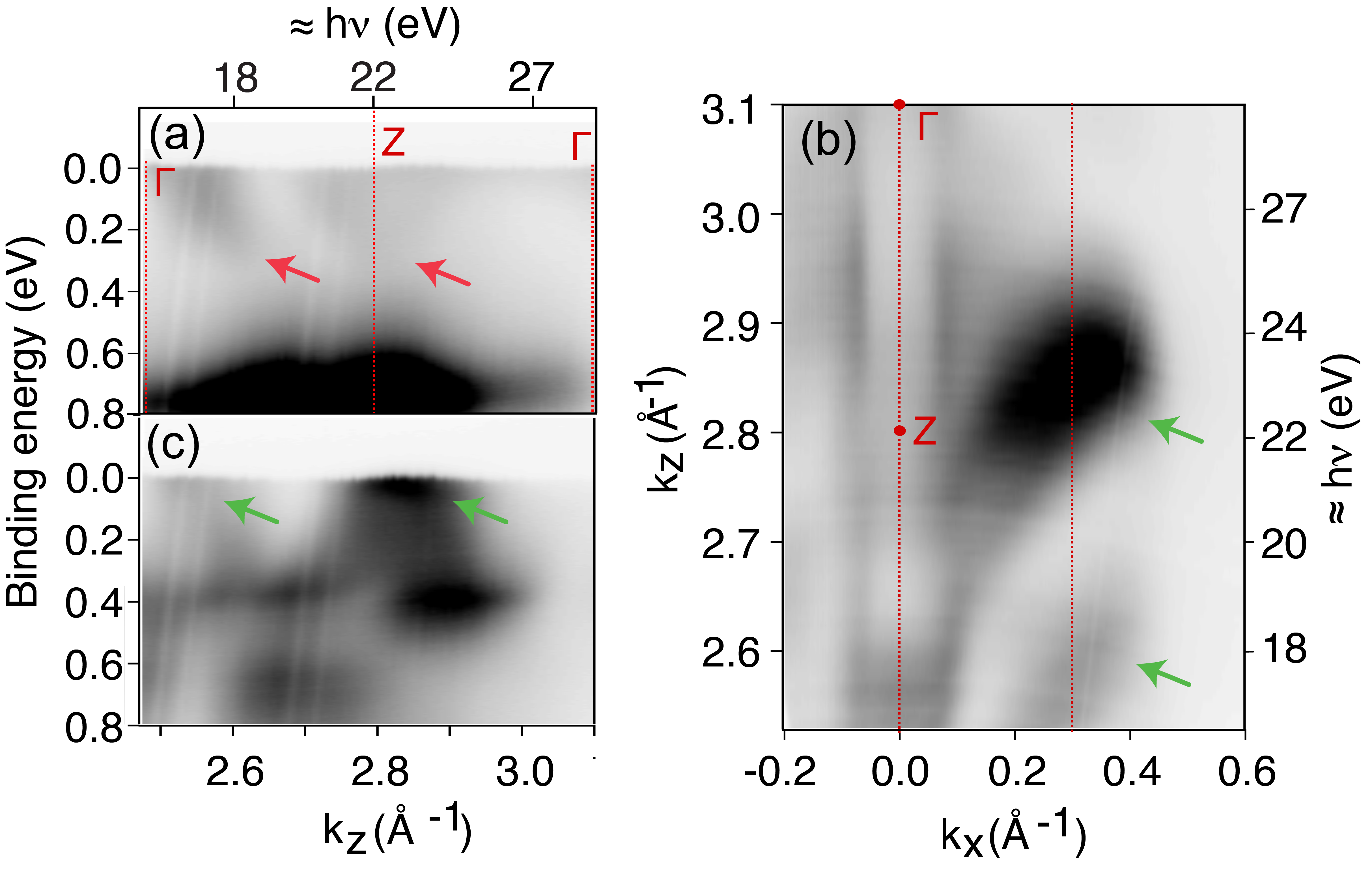
A more systematic investigation of the -dependent bulk band structure in the plane is shown in Figure 2. Here, of the outgoing photoelectrons and thereby also the -dependence of the initial states is explored by collecting photon energy-dependent data. The photon energies have been converted into values using a free electron final state model. Assuming a work function of eV Hao et al. (2012) and an inner potential of eV reproduces the position of a point at eV. The corresponding value is 2.795 Å-1 which is 9 times the bulk distance. The same point is observed at a photon energy of eV for Bi2Se3. For higher photon energies, we find indications of points at and 74.8 eV (not shown). These also agree with the free electron final state model.
Figure 2(a) shows the photoemission intensity as a function of binding energy and collected in normal emission. The data are similar to the corresponding observation for Bi2Se3 (see Figure 6 in Ref. Bianchi et al. (2012a)). A broad parabolic feature is visible near , reaching its highest binding energy at 2.8 Å-1 (red arrow). We identify this as the bottom of the uppermost VB at . A similar structure is visible at lower , reaching the highest binding energy at around 2.6 Å-1 (also marked by a red arrow). These observations are consistent with the position of the uppermost VB in Figure 1(c) and (d) since the two values correspond to photon energies of 18 and 22 eV, respectively. However, the free electron final state model cannot explain the observation of the upper VB minimum at eV ( 2.6 Å-1, as seen in Figures 1(c) and 2(b)), as this value does not correspond to a point. A similar feature for Bi2Se3 was assigned to a surface umklapp process Bianchi et al. (2012a). The same explanation may hold here but the emission could also occur via the non-free electron like nature of the final states at the low photon energies used here.
Having identified the bulk point in the data, we move our attention to the VBM in the plane that is expected to be found at a similar . To this end, Figure 2(b) shows the photoemission intensity at the Fermi energy as a function of and along . Pronounced features are the two vertical streaks that correspond to the Fermi level crossings of the topological surface state. In addition, two dispersive broad structures are visible around Å-1 and at values around 2.6 and 2.8 Å-1 (marked by green arrows). These stem from the VBM in the plane and are also seen in Figures 1(c) and (d). The shape of the high intensity features agrees remarkably well with the calculated constant energy contours for the VB in Figure 3 of Ref. Nechaev et al. (2015). Figure 2(c) shows the dispersion of these structures (also marked by green arrows) with by plotting the photoemission intensity as a function of photon energy in the same way as in Figure 2(a) but for Å-1. The dispersion with is evident. As in the selected data of Figure 1(d), it appears as if the band barely reaches the Fermi level without actually crossing it. This view is also supported by the lack of sharp structures in Figure 2(b) such that the “islands” of high intensity can be interpreted as a spill-out of the intensity from band maxima below , rather than distinct crossings.
In order to confirm this interpretation and to investigate the position of the VB along further, we gain access to the usually unoccupied band structure by adsorbing a low coverage of Rb atoms onto the surface while collecting ARPES data. This leads to doping with electrons and to a downward band bending at the surface Bianchi et al. (2012b). We can track the occupation of the topological surface state and the normally unoccupied VB, and even populate the bottom of the conduction band. We perform the doping experiment at two photon energies, 22 eV and 18 eV to be close to the point expected for free electron final states at 22 eV and to the point-like features reached at 18 eV.
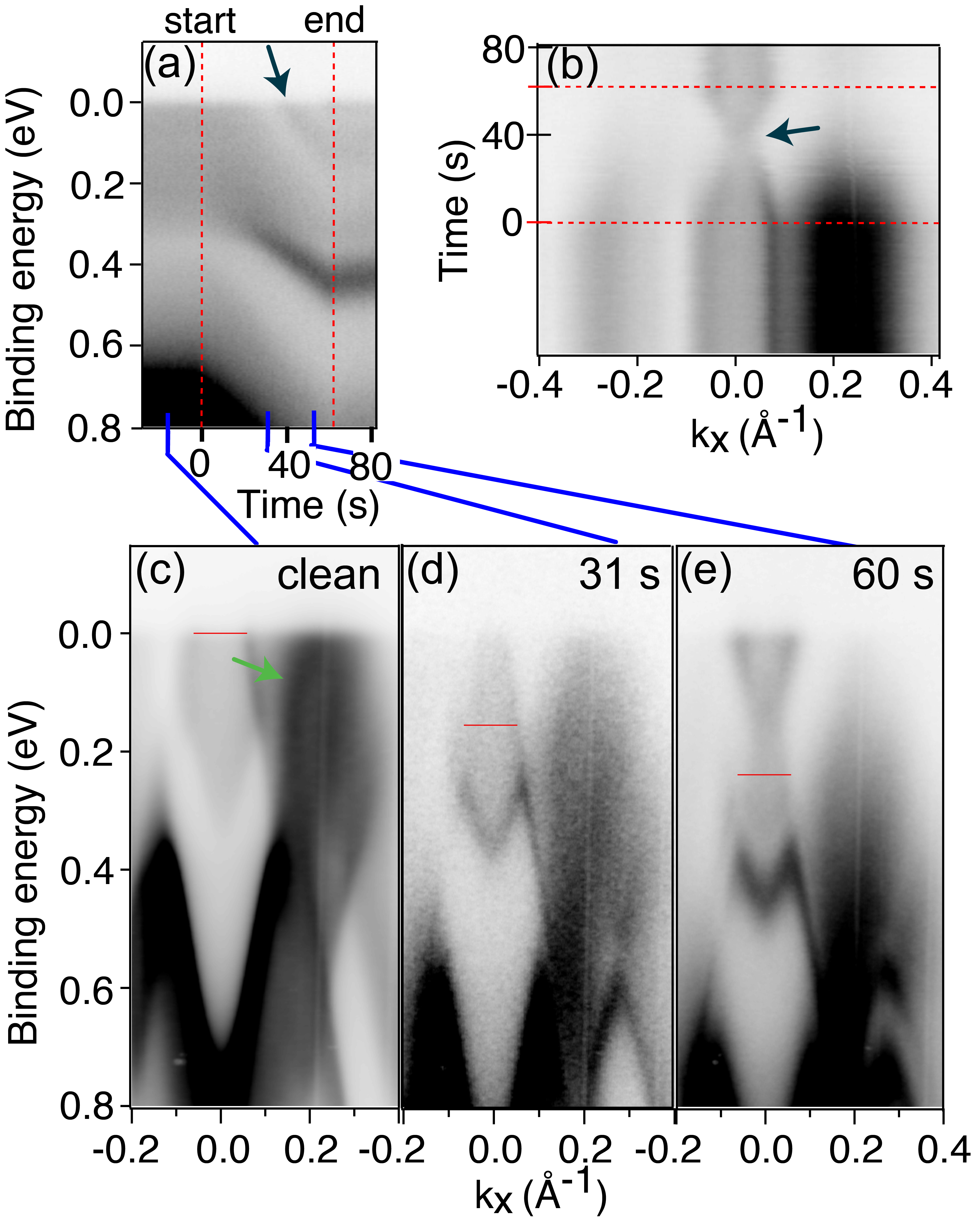
Figure 3(a) shows the photoemission intensity at normal emission for eV as a function of time while dosing Rb atoms onto the surface. The beginning and end of the Rb exposure are marked on the time axis. Figure 3(b) gives the corresponding photoemission intensity at the Fermi energy and along . Figures 3(c)-(e) show snapshots of the electronic structure at selected times. Figure 3(c) was acquired prior to starting the Rb deposition and is thus very similar to Figure 1(d). The band forming the VBM along is marked by a green arrow. Upon Rb dosing the observed bands shift to higher binding energy. After the end of the exposure, the features gradually move back to lower binding energy. This could either be due to Rb desorption or intercalation. Scanning the UV light spot across the sample shows that the shift takes place over the entire sample surface and is not induced by the UV radiation. The amount of Rb present on the sample surface after 60 s of deposition was estimated to be 0.1 monolayer, determined from the ratio between Rb and Te core level photoemission intensities.
As discussed above and seen in Figures 3(a) and (c), the uppermost VB at normal emission appears to be a broad feature between and a binding energy of 300 meV. However, when exposing the surface to Rb, the VB features sharpen up and the photoemission intensity is concentrated in a narrow window around the bottom of the band. This can be explained by a quantisation of the VB states due to a downward bending of the bands near the surface, as such a quantization removes the broadening. Naively, a quantisation upon downward bending of the band is expected for the conduction band, not for the VB, but for this class of materials the VB width is so small that the bands become confined once the amount of band bending exceeds the width of the VB, as has been shown for Bi2Se3 Bianchi et al. (2011). The VB quantisation turns the three-dimensional dispersion into two-dimensional sub-bands that no longer disperse in . The precise location of the VBM at therefore remains inaccessible. We tentatively place the VBM just below the Dirac point. This is consistent with previous observations Pauly et al. (2012) and also with the fact that a weak diffuse photoemission intensity remains inside the lower part of the surface state Dirac cone in Figures 3(d) and (e).
After a Rb exposure time of 32 s, an additional band can be observed to cross and move to high binding energies in Figure 3(a) (black arrow). It originates from the Dirac point of the topological surface state. This can be clearly seen when inspecting the time dependence of the photoemission intensity at shown in Figure 3(b), where the lines representing the Fermi level crossings of the topological surface states start to converge upon Rb dosing and cross at the same time as the state in Figure 3(a) becomes visible, bringing the Dirac cone from the hole-doped to the electron-doped regime. Note also that the intensity at around 0.3 Å-1 vanishes in Figure 3(b) upon doping. As these features correspond to the VBM in the plane, such a shift suggests that the VBM is at higher binding energy than the Dirac point. Inspecting energy- and -dependent spectra at different Rb coverages (Figures 3(c)-(e)) appears to confirm this.
A similar behaviour is observed in Figure 4 where doping-dependent ARPES data acquired at 18 eV is shown. The data are presented in the same way as in Figure 3 and the conclusions about the position of the VBM in the plane are largely the same. The band dispersion is less clear, even for the clean surface. Nevertheless, the photoemission intensity from the VBM along seen in Figure 3(b) quickly vanishes in Figure 4(b) and the band maximum can be clearly placed below the surface state Dirac point. An important difference to Figure 3 is that the Rb exposure was carried out for a longer time (120 s, giving rise to a coverage of 0.3 monolayers). As seen in Figure 3(e), this leads to an occupation of the conduction band (possibly present as a quantized state). Note that the observation of conduction band states does not permit the determination of the bulk band gap, as the conduction band minimum is not found at but close to Nechaev et al. (2015). Furthermore, alkali-induced surface doping does not necessarily conserve the gap size as seen by comparing refs. Miwa et al. (2015) and Grubišić Čabo et al. (2015), for instance.
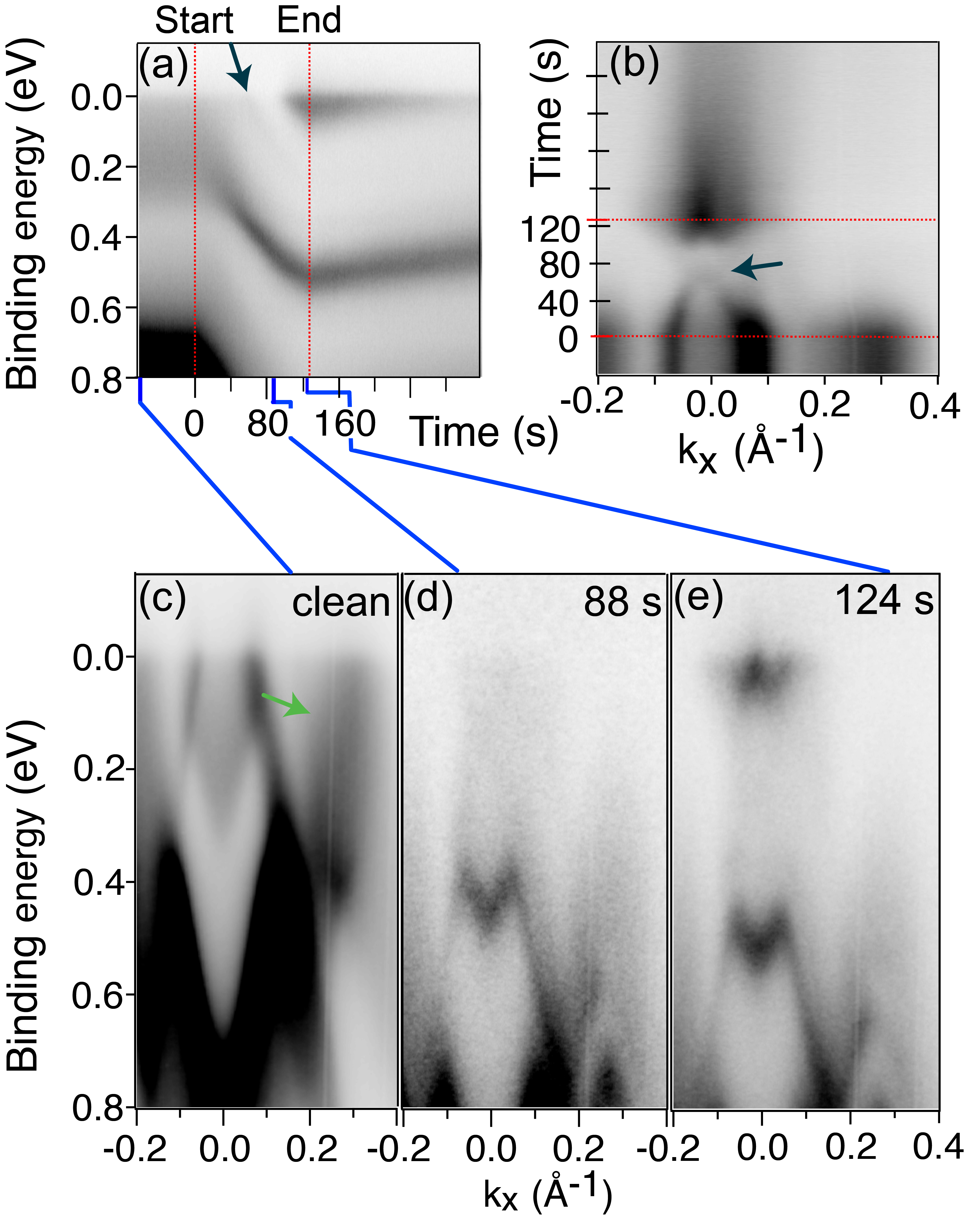
Combining the data for the clean and Rb-covered surface, we can conclude the following about the VB in the plane: The plane does indeed contain a local VBM. However, its energy is lower than that of the global VBM at the point, which we assume to be just below the Dirac point of the surface state. The dispersion of the upper VB in shows a maximum 30 meV below for data taken at 22 eV (see Figures 1(d) and 3(c)). This feature broadens out upon Rb dosing but we do not find any indication of a higher lying maximum.When determining the position of the surface state Dirac point by extrapolation of the linear dispersion above for the clean surface, we find the VBM to be 170 meV 43 meV below the surface state Dirac point. These findings clearly support the dispersion obtained by GW calculations Nechaev et al. (2015). We can rule out the DFT results which place the VBM above the surface state Dirac point Hsieh et al. (2009); Menshchikova et al. (2011).
IV Conclusions
In conclusion, we have determined the band structure of the topmost VB of Sb2Te3 by synchrotron radiation-based angle-resolved photoemission spectroscopy, with the objective to find the position of the global VBM. We find a predicted VBM in the BZ plane given by the azimuthal direction. The binding energy of this band is below the surface state Dirac point. This is significantly different from predictions by DFT but in line with calculations employing GW corrections. The high binding energy of the local VBM implies that it should be possible to achieve surface state dominated electronic transport near the Dirac point for Sb2Te3.
Acknowledgements.
This work was supported by VILLUM FONDEN via the Centre of Excellence for Dirac Materials (Grant No. 11744). S. U. acknowledges financial support from VILLUM FONDEN under the Young Investigator Program (grant no. 15375). We thank Anton Tamtögl for fruitful discussions.References
- Zhang et al. (2009) H. Zhang, C.-X. Liu, X.-L. Qi, X. Dai, Z. Fang, and S.-C. Zhang, Nature Physics 5, 438 (2009).
- Hsieh et al. (2009) D. Hsieh, Y. Xia, D. Qian, L. Wray, F. Meier, J. H. Dil, J. Osterwalder, L. Patthey, A. V. Fedorov, H. Lin, et al., Physical Review Letters 103, 146401 (pages 4) (2009).
- Ando (2013) Y. Ando, Journal of the Physical Society of Japan 82, 102001 (2013).
- Horák et al. (1988) J. Horák, Z. Starý, and J. Klikorka, physica status solidi (b) 147, 501 (1988).
- Hasan and Kane (2010) M. Z. Hasan and C. L. Kane, Rev. Mod. Phys. 82, 3045 (2010).
- Seibel et al. (2012) C. Seibel, H. Maaß, M. Ohtaka, S. Fiedler, C. Jünger, C.-H. Min, H. Bentmann, K. Sakamoto, and F. Reinert, Phys. Rev. B 86, 161105 (2012).
- Reimann et al. (2014) J. Reimann, J. Güdde, K. Kuroda, E. V. Chulkov, and U. Höfer, Phys. Rev. B 90, 081106 (2014).
- Jiang et al. (2012a) Y. Jiang, Y. Wang, M. Chen, Z. Li, C. Song, K. He, L. Wang, X. Chen, X. Ma, and Q.-K. Xue, Phys. Rev. Lett. 108, 016401 (2012.
- Fu et al. (2007) L. Fu, C. L. Kane, and E. J. Mele, Physical Review Letters 98, 106803 (pages 4) (2007).
- Nechaev et al. (2015) I. A. Nechaev, I. Aguilera, V. De Renzi, A. di Bona, A. Lodi Rizzini, A. M. Mio, G. Nicotra, A. Politano, S. Scalese, Z. S. Aliev, et al., Phys. Rev. B 91, 245123 (2015).
- Menshchikova et al. (2011) T. V. Menshchikova, S. V. Eremeev, and E. V. Chulkov, JETP Letters 94, 106 (2011).
- Kioupakis et al. (2010) E. Kioupakis, M. L. Tiago, and S. G. Louie, Phys. Rev. B 82, 245203 (2010).
- Yazyev et al. (2012) O. V. Yazyev, E. Kioupakis, J. E. Moore, and S. G. Louie, Phys. Rev. B 85, 161101 (2012).
- Nechaev and Chulkov (2013) I. A. Nechaev and E. V. Chulkov, Physical Review B 88, 165135 (2013).
- Aguilera et al. (2013) I. Aguilera, C. Friedrich, G. Bihlmayer, and S. Blügel, Physical Review B 88, 045206 (2013).
- Förster et al. (2016) T. Förster, P. Krüger, and M. Rohlfing, Phys. Rev. B 93, 205442 (2016).
- Vidal et al. (2011) J. Vidal, X. Zhang, L. Yu, J.-W. Luo, and A. Zunger, Phys. Rev. B 84, 041109 (2011).
- Zhang et al. (2010) W. Zhang, R. Yu, H.-J. Zhang, X. Dai, and Z. Fang, New Journal of Physics 12, 065013 (2010).
- Nechaev et al. (2013) I. A. Nechaev, R. C. Hatch, M. Bianchi, D. Guan, C. Friedrich, I. Aguilera, J. L. Mi, B. B. Iversen, S. Blügel, P. Hofmann, et al., Phys. Rev. B 87, 121111 (2013).
- Michiardi et al. (2014) M. Michiardi, I. Aguilera, M. Bianchi, V. E. de Carvalho, L. O. Ladeira, N. G. Teixeira, E. A. Soares, C. Friedrich, S. Blügel, and P. Hofmann, Phys. Rev. B 90, 075105 (2014).
- Barreto et al. (2014) L. Barreto, L. Kühnemund, F. Edler, C. Tegenkamp, J. Mi, M. Bremholm, B. B. Iversen, C. Frydendahl, M. Bianchi, and P. Hofmann, Nano Letters 14, 3755 (2014).
- Pauly et al. (2012) C. Pauly, G. Bihlmayer, M. Liebmann, M. Grob, A. Georgi, D. Subramaniam, M. R. Scholz, J. Sánchez-Barriga, A. Varykhalov, S. Blügel, et al., Phys. Rev. B 86, 235106 (2012).
- Seibel et al. (2015) C. Seibel, H. Maaß, H. Bentmann, J. Braun, K. Sakamoto, M. Arita, K. Shimada, J. Minár, H. Ebert, and F. Reinert, Journal of Electron Spectroscopy and Related Phenomena 201, 110 (2015).
- Wang et al. (2010) G. Wang, X. Zhu, J. Wen, X. Chen, K. He, L. Wang, X. Ma, Y. Liu, X. Dai, Z. Fang, et al., Nano Research 3, 874 (2010).
- Plucinski et al. (2013) L. Plucinski, A. Herdt, S. Fahrendorf, G. Bihlmayer, G. Mussler, S. Döring, J. Kampmeier, F. Matthes, D. E. Bürgler, D. Grützmacher, et al., Journal of Applied Physics 113, 053706 (2013).
- Jiang et al. (2012b) Y. Jiang, Y. Y. Sun, M. Chen, Y. Wang, Z. Li, C. Song, K. He, L. Wang, X. Chen, Q.-K. Xue, et al., Phys. Rev. Lett. 108, 066809 (2012.
- Ruckhofer et al. (2021) A. Ruckhofer, S. Halbritter, H. E. Lund, A. J. U. Holt, M. Bianchi, M. Bremholm, G. Benedek, P. Hofmann, W. E. Ernst, and A. Tamtögl, Physical Chemistry Chemical Physics 23, 7806 (2021).
- Hoffmann et al. (2004) S. V. Hoffmann, C. Søndergaard, C. Schultz, Z. Li, and P. Hofmann, Nuclear Instruments and Methods in Physics Research, A 523, 441 (2004).
- Bianchi et al. (2010) M. Bianchi, D. Guan, S. Bao, J. Mi, B. B. Iversen, P. D. C. King, and P. Hofmann, Nature Communications 1, 128 (2010).
- Hao et al. (2012) G. Hao, X. Qi, G. Wang, X. Peng, S. Chang, X. Wei, and J. Zhong, RSC Advances 2, 10694 (2012).
- Bianchi et al. (2012a) M. Bianchi, R. C. Hatch, D. Guan, T. Planke, J. Mi, B. B. Iversen, and P. Hofmann, Semiconductor Science and Technology 27, 124001 (2012.
- Bianchi et al. (2012b) M. Bianchi, R. C. Hatch, Z. Li, P. Hofmann, F. Song, J. Mi, B. B. Iversen, Z. M. Abd El-Fattah, P. Löptien, L. Zhou, et al., ACS Nano 6, 7009 (2012.
- Bianchi et al. (2011) M. Bianchi, R. C. Hatch, J. Mi, B. B. Iversen, and P. Hofmann, Phys. Rev. Lett. 107, 086802 (2011).
- Miwa et al. (2015) J. A. Miwa, S. Ulstrup, S. G. Sørensen, M. Dendzik, A. G. Čabo, M. Bianchi, J. V. Lauritsen, and P. Hofmann, Phys. Rev. Lett. 114, 046802 (2015).
- Grubišić Čabo et al. (2015) A. Grubišić Čabo, J. A. Miwa, S. S. Grønborg, J. M. Riley, J. C. Johannsen, C. Cacho, O. Alexander, R. T. Chapman, E. Springate, M. Grioni, et al., Nano Letters 15, 5883 (2015).