Isochronous Data Link Across a Superconducting Nb Flex
Cable
with 5 femtojoules per Bit
Abstract
Interconnect properties position superconducting digital circuits to build large, high performance, power efficient digital systems. We report a board-to-board communication data link, which is a critical technological component that has not yet been addressed. Synchronous communication on chip and between chips mounted on a common board is enabled by the superconducting resonant clock/power network for RQL circuits. The data link is extended to board-to-board communication using isochronous communication, where there is a common frequency between boards but the relative phase is unknown. Our link uses over-sampling and configurable delay at the receiver to synchronize to the local clock phase. A single-bit isochronous data link has been demonstrated on-chip through a transmission line, and on a multi-chip module (MCM) through a superconducting tape between driver and receiver with variable phase offset. Measured results demonstrated correct functionality with a clock margin of 3 dB at 3.6 GHz, and with 5 fJ/bit at 4.2 K.
Superconducting digital circuits have the potential to enable digital systems with very high computation density [1]. The combination of low power logic [2] and low loss interconnects (e.g. [3] and references thereof) shifts the design trade-off towards heterogeneous distributed architectures with multiple chips on multiple boards. Volumetric cooling with efficient heat transfer allows such a system to be physically small, with packing density limited only by the physical dimensions of the connectors on the boards. Superconducting systems trade modest chip integration density for high packaging density.
Efficient distributed heterogeneous architectures require tremendous communication bandwidth on-board and board-to-board. Design challenges involve both the interconnects themselves, and synchronization between driver and receiver. Nb interconnects having 700 GHz analog bandwidth can cover distance with appropriate data encoding and geometry of the wires [4]. A bandwidth-efficient driver producing 10 SFQ pulses per bit, with an analog bandwidth of 35 GHz and 0.58 fJ per bit has been reported in [5]. This bandwidth-efficient driver has been used to demonstrate synchronous communication between 1010 mm chips on an MCM with interconnect length up to 54 mm. Superconducting Nb flex tape on Polyimide has been proposed for board-to-board communication [6], [7]. Tape enables longer range communication relative to MCM because of very low dielectric losses, , at cryo temperatures [8] and due to relatively large dimensions for the traces and dielectric thickness. The 35 Gb/s serial bandwidth of such tape is five times higher than state-of-the-art CMOS (e.g., [9] and references thereof) at three orders of magnitude less power dissipation while including a cryocooler overhead of 300 W/W.
Superconducting RQL technology also provides a simple and robust way to implement synchronization between boards. RQL uses a synchronous resonator-based clock distributed across chips on the MCM [10]. The resonators at 4.2 K have a high quality factor of 500 that ensures stability, have 30% efficiency, and are driven by precise external frequency sources. These features allow RQL to support isochronous communication between multiple boards, driven at the same frequency but with an arbitrary phase relationship between them. The receiver identifies the relative phase between boards during initialization, and adjusts the data link accordingly. This scheme is quite simple and lightweight compared to standard SerDes receivers, without the large overhead in hardware and power dissipation.
In this paper we present the design of the isochronous receiver, consisting of 1) an analog circuitry performing oversampling of input signal using four available phases of RQL clock, and 2) a digital block performing arbitration among the phases. The isochronous communication link is first characterized experimentally for functionality and operating margin using a test circuit with on-chip interconnects, and then characterized over an MCM and over a 20 mm Nb flex tape, with two separate resonators with tunable relative phases for driver and receiver.
I Isochronous receiver data link
The isochronous board-to-board link is based on the feature that the resonators on all boards in the system are powered by a common high-precision clock source. In this scenario there is no relative phase drift in the system, but there is a static and unknown phase offset between boards due to variability e.g., in cable length. The phase offset is established at the receiver during initialization. The phase can be reset with reinitialization but this is not done in normal operation. Initialization is achieved with a global training sequence, e.g. provided by a scan chain passing though all boards. The training data are oversampled using the four phases of the RQL AC clock, and the phase difference is established using logical aligning block. One control block per bus is sufficient. Currently the receiver design resolves 90∘ phase granularity and has three cycles of latency. Increasing the oversampling ratio increases phase granularity at the expense of latency and complexity.
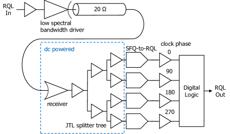
The isochronous receiver one-bit link shown in Fig. 1 consists of a bandwidth-efficient driver, a 20 line, and an oversampling receiver. The bandwidth-efficient driver is a self-resetting gate as described in [5]. The driver latches to produce a Gaussian waveform of about 10 underlying SFQ pulses per bit. The driver significantly increases signal propagation distance by reducing high frequency analog content and the associated dispersion. The driver supports up to 10 Gb/s serial data rate. The 20 line is a Nb passive transmission line (PTL) resistively terminated at the receiver. The PTL can be implemented as a stripline on a Si substrate or cable flexible substrate. The particular implementations used in the current experiments are discussed below.
The isochronous oversampling receiver circuit consists of a DC-biased block used to receive the signal at arbitrary timing, followed by an AC-biased block used to align the incoming pulse to a particular phase of the global clock. The DC-biased receiver is sensitive only to positive-polarity signals. The negative-polarity trailing pulse generated by the driver is terminated at the receiver and lost. The receiver is DC-powered to guarantee that signal will be captured despite arbitrary timing relative to the RQL AC clock. The receiver consists simply of a two-junction Josephson transmission line with 35 A and 50 A critical currents as described in [5].
The received signal is fed to a DC-powered four-way splitter. Oversampling is realized by feeding these signals in parallel to four SFQ-to-RQL converters that are AC-biased with the four RQL clock phases. For those phases with good timing relative to the incoming signal, the SFQ-to-RQL stage converts the positive SFQ into a bipolar RQL signal. Based on the relative timing of the incoming signal and the RQL phases, one or two converters will succeed.
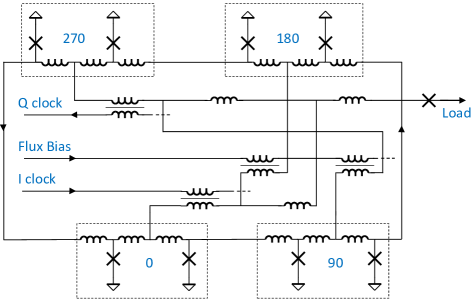
DC bias could be supplied externally and in parallel to all receivers, but to achieve a scalable solution we instead use a Josephson AC-to-DC converter on-chip, called a “flux-pump.” The AC-to-DC converter acts as a current-limited voltage source. The maximum voltage corresponds to one SFQ pulse per clock cycle—just enough to power the receiver, which consumes up to one SFQ per clock cycle from the bias line, when fully active. The current-limit is by default a strong function of the applied AC bias level. A floating Josephson junction in series with the load can be used to regulate the current. A flux-pump circuit function has been described in [11]. As a primary figure of merit for the flux pump is high current compliance across parameter variations, we use our own design, shown in Fig. 2.
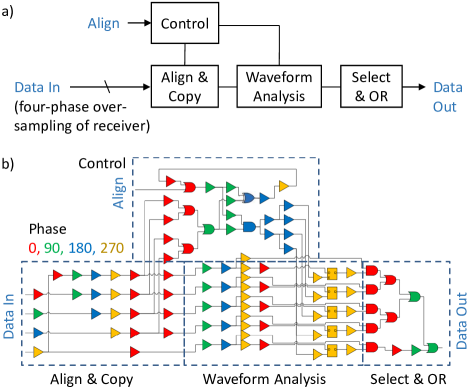
The digital portion of the isochronous receiver, illustrated in Fig. 3, aligns the incoming signal with the local clock phase by selecting among paths of differing delay. The different path lengths are generated in the “Align & Copy” block. One or two contiguous paths are selected by the D-latches (squares) in the “Waveform Analysis” block. The “Select & OR” block ANDs the incoming data with the state of each latch, and ORs these results to produce the final output. The incoming data constantly provides input to the D-latches, but their state is set only when the Align signal associated with the “Control” block enables them. When the latches are enabled, an isolated pilot pulse on the data input sets the latches associated with the correct path delays, which are those that succeed in picking up the input signal.
Five delay paths are used as the delay wraps around from 0∘ to 360∘. A signal in the gray zone between clock cycles may be configured for minimum delay or for one additional cycle. However, once the link is configured, the selection will be maintained for subsequent data.
Extension to a multi-bit bus could be achieved by replicating the receiver. If all the lines in the bus are equal in length, a common control block associated with just one of the bits would be needed to configure all the bits.
II Test vehicle

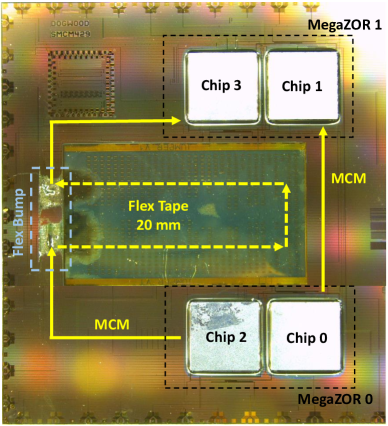
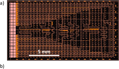
We have designed three experiments to test the isochronous communication link with data transfer using on-chip PTL, on-carrier PTL, and Nb flex cable, as shown in Fig. 4a. The on-chip data link is for measuring the operating margins of on-chip circuitry. The two experiments with on-carrier link and Nb flex cable link allow to test complete functionality of the isochronous link including phase alignment. These experiments use a multi-chip module (MCM) with four chips mounted on superconducting carrier as shown in Fig. 4b.
The on-chip circuitry has all components as described in the previous section. The on-chip data link is configured to be tested on individual die prior to die attach on MCM. It contains 22 mm long, 20 on-chip transmission line with propagation delay targeting a gray zone between 0∘ and 270∘ phase. This case represents the most complicated regime of phase alignment resolving the phase difference at the boundary between two clocks. The data link circuit is wrapped with the on-chip test bed (see Fig. 4a) consisting of two differential inputs [2] for data and align signals and a single 4 mV differential output amplifier [12]. The whole circuit is powered by an on-chip resonant clock network covering the active area of the chip. The circuit has common AC bias and DC flux lines for all components. The test circuit was designed to operate at 3.4 GHz, which is lower than the 10 GHz target for the design of the data link itself. The lower operating frequency allows feasibility demonstration using the simple fabrication process and design flow that was not targeted to aggressive timing. Simulation waveforms are shown in Fig. 5. The simulated circuit operating margin for AC bias is 5 dB (30%) with junction critical current margins of individual gates at 50%. The isochronous receiver contains about 600 Josephson junctions with total power dissipation less than 5 fJ per bit including all receiver overhead and a cryocooler efficiency of 300 W/W.
The chip was designed into the fabrication process at D-Wave with 0.25 m feature size and six metal layers [13], and with a modified critical current density of 100 A/m2. The minimum critical current in the circuit is 35 A. The analog portion of the circuit consisting of the driver, flux pumps and DC receiver, was designed using a custom design flow in the Cadence environment based on Spectre analog simulations and inductor P-cell based layout. The digital block was designed using automated Cadence based digital flow including synthesis, placement, timing and logical verification. A custom inductance-target router was used. Final chip-level verification includes Spectre simulations as well as DRC and LVS with custom checks for parasitic coupling.
For the MCM phase alignment experiments we used the well-characterized process for the carrier and bump-bonds developed at Lincoln Laboratory [14]. The “smcm4m” four Nb metal process supports the design of both 20 data PTLs and the clock resonator network, isolated using a superconducting ground plane. The In bump bonding process, with 15 m bump diameter, 35 m bump pitch, and about 3 m bump height post-bonding, supports MCM-to-chip transitions with 350 GHz analog bandwidth [5].
The 3232 mm MCM carrier for the phase align experiments with both on-carrier PTL and Nb flex cable, contains two separate “megaZOR” resonator networks, with independent control of frequency and amplitude. Each MegaZOR is a resonator of segments on the MCM designed to drive several on–chip ZOR resonators as described in [5]. The carrier MegaZOR design has been targeted to match the experimental average resonance frequency of the individual chips. The MegaZOR was optimized to achieve less than 1 dB amplitude variation and less than 5∘ phase variation between two chips with worst-case % speed of light variation across the carrier and % variation in resonance frequency between individual chips.
The superconducting flexible ribbon cable has been designed at Auburn University [6, 7] and fabricated by Hightec, a commercial manufacturer. The cable is a stack-up of thin-film polyimide layers (PI2611 from HD Microsystems) and patterned Nb metal. There are three Nb metal layers building 86 m-wide stripline interconnects with high isolation. The signal traces were designed by Auburn to be 20 , matching the other link components. For the current experiment, the custom tape has all wires in loop-back as shown in Fig. 6a.
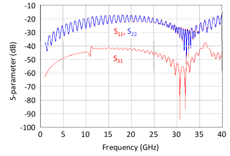
The transition between MCM and flex tape is done using a second In bump-bond process with 75 m bumps at 150 m pitch [15]. The transition between cable and MCM has been optimized using HFSS 3D field solver with requirements of less than dB reflection and less than dB coupling between adjacent pins, as shown in Fig. 6b. Full system simulations in Spectre have been done to verify circuit operating margin using the S-parameter matrix for the MCM-flex transition extracted from HFSS model. The operating margin for the circuit is comparable to on-chip link simulations.
III Test results
Candidate chips from the same wafer were characterized individually for parameter targeting using PCM data and for resonator performance following procedures explained in [10]. The PCM measurements indicated that the Josephson junction critical current and routing inductances are within tolerances of 10% and 2% respectively. The average wafer resonant frequency of 3.6 GHz is within 6% of the 3.4 GHz design target. S-parameters for the resonator showed less than 40 dB coupling and coincident resonant peaks between I and Q resonators.
The selected chips were tested for functionality of the on-chip data link. The test was performed at the resonance frequency in liquid He using a pressure-contact dip probe and a custom electronics rack. The digital vectors were generated using Keysight M8020 synchronized with a Rhode & Schwartz SGS100A frequency generator. The output data link was as described in [12]. The output signal was captured on a Tektronix MSO7204C oscilloscope, and an automated procedure for collecting 2D margins of AC clock amplitude vs. JTL bias was applied.
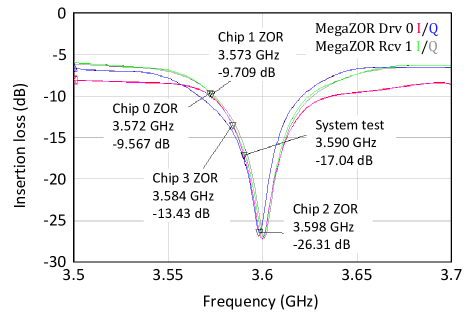
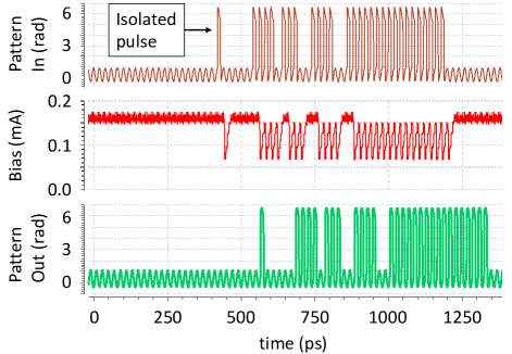
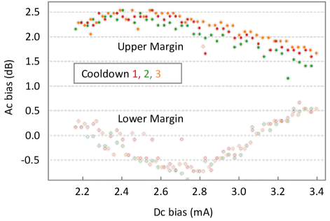
Fig. 7 shows experimental 2D operating margin on the bias. The test pattern starts with align input bit and data alignment pattern with an isolated bit, followed by nine zeros. The data test pattern consists of four ones followed by four zeros and 16 ones. The same test pattern is repeated for each point for 2D margin collection. The chip has about 3 dB AC clock margin at optimum JTL bias of 2.75 mA. This chip exhibits 0.5 dB variation across cooldowns, which is within design tolerances for coupling to parasitic flux vortexes sequestered in the moats. Margin degradation of 2 dB relative to simulations is within the typical budget for the fabrication process and layout style, with contributions including variation in fabrication parameters, resonator uniformity, and cross-net coupling in the digital routing.
The carrier was selected from a wafer with 16 3232 mm instances. Each carrier was characterized using on-carrier PCMs containing a chain of the MCM bumps for DC measurements of critical current, and a resonator for speed-of-light measurements for data and resonator metal layers. PCM results showed 100% yield on DC bump chains with more than 32 mA critical current and about 3% resonance frequency variation across the wafer with the best die being within 1% of the design target. Test results of S-parameter characterization of each MegaZOR are shown in Fig. 8.
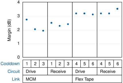
Fig. 9 shows experimentally-measured margins for two data links on the MCM configured to 90∘ static phase offset between driver and receiver. The same test pattern has been used as for the individual on-chip link. Both links showed complete functionality with operating margin of 2.8 dB on-carrier and 3.5 dB on the flex cable. Operating margins for both links are on par with on-chip PTL test and stable across cool downs. The best margin of 3.5 dB is for the data link over the flex cable, which can be accounted for by low-loss in the polyimide dielectric compared to SiO2 dielectric on the carrier, and by the wider geometry of the flex Nb signal lines with less dispersion.
IV Conclusion
We have presented the first practical circuit for superconducting board-to-board communication, based on an isochronous data link enabled by the resonant clock of RQL circuits. The data link was demonstrated with a 20 mm Nb flex tape mounted on a superconducting MCM. The 3 dB margin of the flex-tape data link was comparable to a similar circuit using superconducting PTLs on the MCM carrier.
The isochronous link explained in this paper is scalable to multi-bit buses and higher frequency. More optimal phase selection at the receiver could be achieved by adding more granularity in phases while leaving the overall design unchanged. For a low skew, multi-bit bus, just one of the bits is required for phase selection, and its digital control block can be shared with the other bits. Where skew between bits exceeds clock phase granularity, the entire digital block needs to be duplicated per bit, or per group. The analog bandwidth of the link is limited by the dispersion and loss in the flex cable. The driver produces data pulses of about 10 SFQ pulses per bit, allowing a data rate of 10 Gb/s, and a flex cable length up to two meters.
Small hardware overhead, energy efficiency, and high throughput of the isochronous link positions RQL technology as a digital technology with high computational density and high cross-sectional bandwidth of the interconnect in a system of multiple boards. In particular, the interconnect could enable flat memory access across the system. Such an architecture has the potential for significant performance gains in systolic arrays for machine learning.
Acknowledgements.
The authors acknowledge the contributions of the Lincoln Laboratory team, particularly Sergey Tolpygo, in technical discussions and assistance with design. We also acknowledge Vaibhav Gupta, Archit Shah and the AMNSTC staff (especially Drew Sellers) at Auburn University for their assistance with fabrication of the flex cables. The Northrop Grumman superconducting digital EDA and PDK teams laid the foundation for digital design of the isochronous receiver. We also acknowledge the contribution of Steve Shauck and Alex Braun for guidance with the digital design.References
- Holmes et al. [2013] D. S. Holmes, A. L. Ripple, and M. A. Manheimer, Energy-efficient superconducting computing–Power budgets and requirements, IEEE Transactions on Applied Superconductivity 23, 1701610 (2013).
- Herr et al. [2011] Q. P. Herr, A. Y. Herr, O. T. Oberg, and A. G. Ioannidis, Ultra-low-power superconductor logic, Journal of Applied Physics 109, 103903 (2011).
- Filippov et al. [2017] T. Filippov, D. Amparo, M. Kamkar, J. Walter, A. Kirichenko, O. Mukhanov, and I. Vernik, Experimental investigation of ERSFQ circuit for parallel multibit data transmission, in 2017 16th International Superconductive Electronics Conference (ISEC) (IEEE, 2017) pp. 1–4.
- Talanov et al. [2021] V. V. Talanov, D. Knee, D. Harms, K. Perkins, A. Urbanas, J. Egan, Q. Herr, and A. Herr, Propagation of picosecond pulses on superconducting transmission line interconnects, arXiv preprint arXiv:2104.07371 (2021).
- Egan et al. [2021a] J. Egan, M. Nielsen, J. Strong, V. V. Talanov, E. Rudman, B. Song, Q. Herr, and A. Herr, Synchronous chip-to-chip communication with a multi-chip resonator clock distribution network, arXiv preprint arXiv:2109.00560 (2021a).
- Tuckerman et al. [2016] D. B. Tuckerman, M. C. Hamilton, D. J. Reilly, R. Bai, G. A. Hernandez, J. M. Hornibrook, J. A. Sellers, and C. D. Ellis, Flexible superconducting Nb transmission lines on thin film polyimide for quantum computing applications, Superconductor Science and Technology 29, 084007 (2016).
- Gupta et al. [2019] V. Gupta, B. Yelamanchili, S. Zou, T. Isaacs-Smith, J. A. Sellers, D. B. Tuckerman, and M. C. Hamilton, Thin-film Nb/Polyimide superconducting stripline flexible cables, IEEE Transactions on Applied Superconductivity 29, 1 (2019).
- Bai et al. [2016] R. Bai, G. A. Hernandez, Y. Cao, J. A. Sellers, C. D. Ellis, D. B. Tuckerman, and M. C. Hamilton, Cryogenic microwave characterization of Kapton polyimide using superconducting resonators, in 2016 IEEE MTT-S International Microwave Symposium (IMS) (IEEE, 2016) pp. 1–4.
- Miller [2017] D. A. Miller, Attojoule optoelectronics for low-energy information processing and communications, Journal of Lightwave Technology 35, 346 (2017).
- Strong and et. al. [2021] J. Strong and et. al., A resonant metamaterial clock distribution network for superconducting logic, to be published (2021).
- Semenov et al. [2014] V. K. Semenov, Y. A. Polyakov, and S. K. Tolpygo, New AC-powered SFQ digital circuits, IEEE Transactions on Applied Superconductivity 25, 1 (2014).
- Egan et al. [2021b] J. Egan, A. Brownfield, and Q. Herr, True differential superconducting on-chip output amplifier, arXiv preprint arXiv:2104.07372 (2021b).
- Berkley et al. [2010] A. Berkley, M. Johnson, P. Bunyk, R. Harris, J. Johansson, T. Lanting, E. Ladizinsky, E. Tolkacheva, M. Amin, and G. Rose, A scalable readout system for a superconducting adiabatic quantum optimization system, Superconductor Science and Technology 23, 105014 (2010).
- Das et al. [2017] R. N. Das, V. Bolkhovsky, S. K. Tolpygo, P. Gouker, L. M. Johnson, E. A. Dauler, and M. A. Gouker, Large scale cryogenic integration approach for superconducting high-performance computing, in 2017 IEEE 67th Electronic Components and Technology Conference (ECTC) (2017) pp. 675–683.
- Peek et al. [2019] S. Peek, V. Gupta, B. Yelamanchili, T. Stegeman, T. Isaacs-Smith, J. A. Sellers, D. B. Tuckerman, and M. C. Hamilton, Fabrication and assembly processes for custom and commercial flip-chip connections to fine pitch In bump arrays, perspective 1, 2 (2019).