captionUnsupported document class
A Cost and Power Feasibility Analysis of Quantum
Annealing for NextG Cellular Wireless Networks
Abstract.
In order to meet mobile cellular users’ ever-increasing data demands, today’s 4G and 5G networks are designed mainly with the goal of maximizing spectral efficiency. While they have made progress in this regard, controlling the carbon footprint and operational costs of such networks remains a long-standing problem among network designers. This paper takes a long view on this problem, envisioning a NextG scenario where the network leverages quantum annealing for cellular baseband processing. We gather and synthesize insights on power consumption, computational throughput and latency, spectral efficiency, operational cost, and feasibility timelines surrounding quantum technology. Armed with these data, we analyze and project the quantitative performance targets future quantum annealing hardware must meet in order to provide a computational and power advantage over CMOS hardware, while matching its whole-network spectral efficiency. Our quantitative analysis predicts that with quantum annealing hardware operating at a 102 s problem latency and 3.1M qubits, quantum annealing will achieve a spectral efficiency equal to CMOS computation while reducing power consumption by 41 kW (45% lower) in a representative 5G base station scenario with 400 MHz bandwidth and 64 antennas, and an 8 kW power reduction (16% lower) using 1.5M qubits in a 200 MHz-bandwidth 5G scenario.
1. Introduction
Today’s 4G and 5G Cellular Radio Access Networks (RANs) are experiencing unprecedented growth in traffic at base stations (BSs) due to increased subscriber numbers and their higher quality of service requirements (cisco, ; nokia, ). To meet the resulting demand, techniques such as Massive Multiple-Input Multiple-Output (MIMO) communication, cell densification, and millimeter-wave communication are expected to be deployed in fifth-generation (5G) cellular standards (3gppintro, ). But this in turn significantly increases the power and cost required to operate RAN sites backed by complementary metal oxide semiconductor (CMOS)-based computation. While research and industry efforts have provided general solutions (e.g., sleep mode (lahdekorpi2017energy, ) and network planning (wu2015energy, )) to increase energy efficiency and decrease power consumption of RANs, the fundamental challenge of power requirements scaling with the exponentially increasing computational requirements of the RAN persists. Previously (ca. 2010), this problem had not limited innovation in the design of wireless networks, due to a rapid pace of improvement in CMOS’s computational efficiency. Unfortunately however, today, such developments are not maintaining the pace they had in past years, due to transistors approaching atomic limits (courtland2016transistors, ) and the end of Moore’s Law (expected ca. 2025–2030 (khan2018science, ; shalf2020future, ; itrs, )). This therefore calls into question the prospects of CMOS to achieve NextG cellular targets in terms of both energy and spectral efficiency.
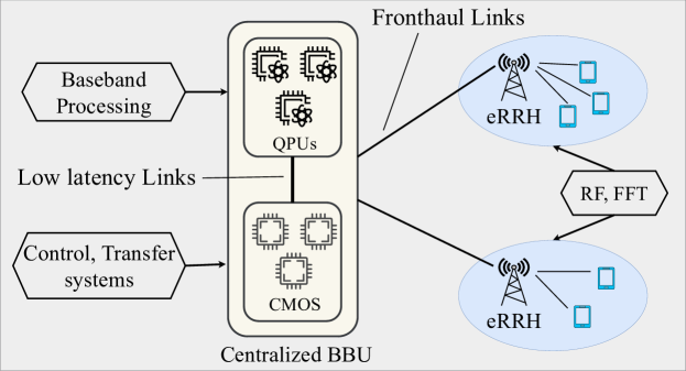
This work investigates a radically different baseband processing architecture for RANs, one based on quantum computation, to see whether this emerging technology can offer cost and power benefits over CMOS computation in wireless networks. We seek to quantitatively analyze whether in the coming years and decades, mobile operators might rationally invest in the RAN’s capital (CapEx) by purchasing quantum hardware of high cost, in a bid to lower its operational expenditure (OpEx) and hence the Total Cost of Ownership (TCO = CapEx + OpEx). The OpEx cost reduction would result from the reduced power consumption of the RAN, due to higher computational efficiency of quantum processing over CMOS processing for certain heavyweight baseband processing tasks. Figure 1 depicts this envisioned scenario, where quantum processing units (QPUs) co-exist with traditional CMOS processing at Centralized RAN (C-RAN) Baseband Units (BBUs) (checko2014cloud, ; 7414384, ). QPUs will then be used for the BBU’s heavy baseband processing, whereas CMOS will handle the network’s lightweight control plane processing (e.g., resource allocation, communication control interface), transfer systems (e.g., enhanced common public radio interface, mobility management entity), and further lightweight tasks such as pre- and post-processing QPU-specific computation.
This paper presents the first extensive analysis on power consumption and quantum annealing (QA) architecture to make the case for the future feasibility of quantum processing based RANs. While recent successful point-solutions that apply QA to a variety of wireless network applications (10.1145/3372224.3419207, ; 9500557, ; kim2019leveraging, ; wang2016quantum, ; cao2019node, ; ishizaki2019computational, ; wang2019simulated, ; chancellor2016direct, ; lackey2018belief, ; bian2014discrete, ; cui2021quantum, ) serve as our motivation, previous work stops short of a holistic power and cost comparison between QA and CMOS. Despite QA’s benefits demonstrated by these prior works in their respective point settings, a reasoning of how these results will factor into the overall computational performance and power requirements of the base station and C-RAN remains lacking. Therefore, here we investigate these issues head-on, to make an end-to-end case that QA will likely offer benefits over CMOS for handling BBU processing, and to make time predictions on when this benefit will be realized. Specifically, we present informed answers to the following questions:
-
Question 1:
How many qubits (quantum bits) are required to realize BS or C-RAN BBU processing requirements? (Answer: cf. §4.3)
-
Question 2:
Relative to purely CMOS BBU processing, how much power and cost does one save with such amount of qubits, viewed over the entire RAN? (Answer: cf. §5)
- Question 3:
-
Question 4:
To what amount will QA processing latency (a performance bottleneck in current QA devices) be reduced in the future? (Answer: cf. §3)
In order to realize the architecture of Figure 1, several key system performance metrics need to be analyzed, quantified, and evaluated, most notably the computational throughput and latency (§3), the power consumption of the entire system and resulting spectral efficiency (bits per second per Hertz of frequency spectrum) and operational cost (§5). Our approach is to first describe the factors that influence processing latency and throughput on current QA devices and then, by assessing recent developments in the area, project what computational throughput and latency future QA devices will achieve (§3). We analyze cost by evaluating the power consumption of QA and CMOS-based processing at equal spectral efficiency targets (§5). Our analysis reveals that a three-way interplay between latency, power consumption, and the number of qubits available in the QA hardware determines whether QA can benefit over CMOS. In particular, latency influences spectral efficiency, power consumption influences energy efficiency, and the number of qubits influences both. Based on these insights, we determine properties (i.e., latency, power consumption, and qubit count) that QA hardware must meet in order to provide an advantage over CMOS in terms of energy, cost, and spectral efficiency in wireless networks.
| B/W | Qubits | Power Consumption | ||||
|---|---|---|---|---|---|---|
| BS | CRAN | BS (KW) | CRAN (MW) | |||
| CMOS | QA | CMOS | QA | |||
| 50 MHz | 386K | 1.16M | 19.3 | 36 | 0.079 | 0.081 |
| 100 | 772K | 2.32M | 29.4 | 37.9 | 0.11 | 0.09 |
| 200 | 1.54M | 4.62M | 49.5 | 41.6 | 0.17 | 0.10 |
| 400 | 3.08M | 9.24M | 89.9 | 49 | 0.29 | 0.13 |
Table 2 summarizes our results, showing that for 200 and 400 MHz bandwidths, respectively, with 1.54 and 3.08M qubits, we predict that QA processing will achieve spectral efficiency equal to today’s 14 nm CMOS processing, while reducing power consumption by 8 kW (16% lower) and 41 kW (45% lower) in representative 5G base station scenarios. In a C-RAN setting with three base stations of 200 and 400 MHz bandwidths, QA processing with 4.62M and 9.24M qubits, respectively, reduces power consumption by 70 kW (41% lower) and 160 kW (55% lower), while achieving equal spectral efficiency to CMOS.
Our further evaluations compare QA against future 1.5 nm CMOS process, which is expected to be the silicon technology at the end of Moore’s law scaling (ca. 2030 (itrs, )). In a base station scenario with 400 MHz bandwidth and 128 antennas, QA with 6.2M-qubits will reduce power consumption by 30.4 kW (37% lower), in comparison to 1.5 nm CMOS, while achieving equal spectral efficiency to CMOS.
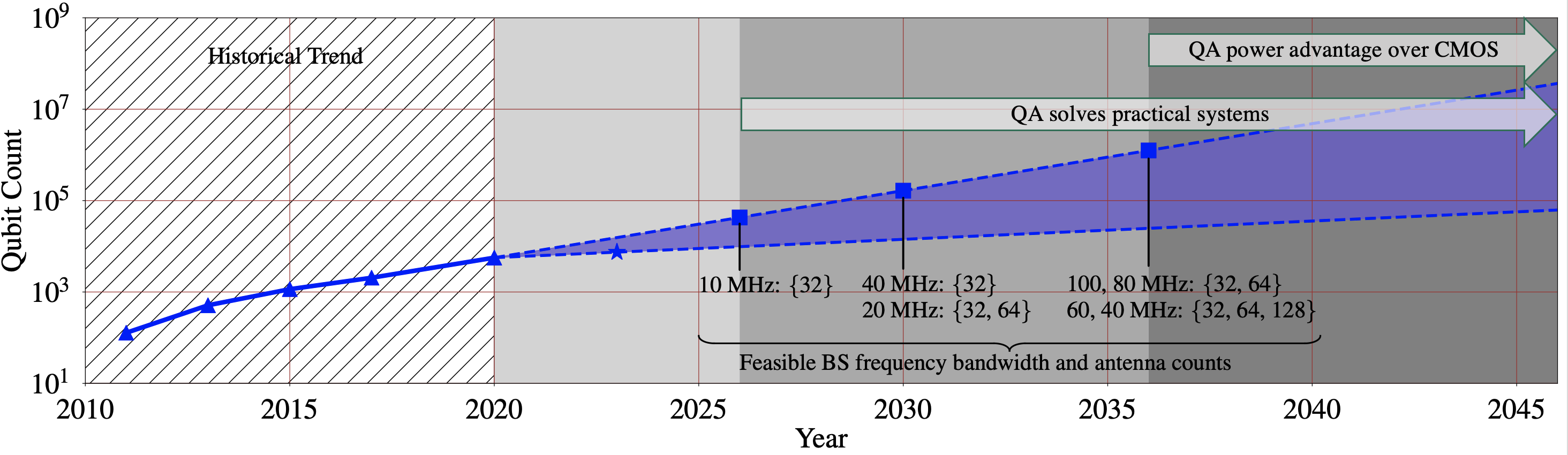
Figure 2 reports our projected QA feasibility timeline, describing year-by-year milestones on the application of QA to wireless networks. Our analysis shows that with custom QA hardware (cf. §2) and qubits growing 2.65 every three years (the 2017–2020 trendline), QA application in practical RAN settings with potential power/cost benefit is a predicted 15 years (ca. 2036) away, whereas the feasibility in processing for a base station (BS) with 10 MHz bandwidth and 32 antennas is a predicted five years away (ca. 2026) (cf. §6).
Overall, our quantitative results predict that QA hardware will offer power benefits over CMOS hardware in certain wireless network scenarios, once QA hardware scales to at least a million qubits (cf. §6) and reduces its problem processing time to hundreds of microseconds, which we argue is feasible within our projected timelines. Scaling QA processors to millions of qubits will pose challenges related to engineering, control, and operation of hardware resources, which designers continue to investigate (boothby2021architectural, ; bunyk-architectural, ). Recent further work demonstrates large-scale qubit control techniques, showing that control of million qubit-scale quantum hardware is already at this point in time a realistic prospect (vahapoglu2021single, ).
Roadmap.
In the remainder of this paper, Section 2 describes background and assumptions, Section 3 analyzes QA hardware architecture and its end-to-end processing latency, and Section 4 describes power modeling in RANs and cellular computational targets. We will then be in a position to present our CMOS versus QA power comparison methodology and results in Section 5. We conclude by discussing a projected feasibility timeline of QA-based RANs in Section 6.
2. Background and Assumptions
While classical computation uses bits to process information, quantum computation uses qubits, physical devices that allow superposition of bits simultaneously (tech, ). The current technology landscape consists broadly of fault-tolerant approaches to quantum computing versus noisy intermediate scale quantum (NISQ) implementations. Fault-tolerant quantum computing (shor1996fault, ; preskill1998fault, ) is an ideal scenario that is still far off in the future, whereas NISQ computing (preskill2018quantum, ), which is available today, suffers high machine noise levels, but gives us an insight into what future fault-tolerant methods will be capable of in terms of key quantum effects such as qubit entanglement and tunneling (preskill2018quantum, ). NISQ processors can be classified into digital gate model or analog annealing (QA) architectures.
Gate-model devices (knill2005quantum, ) are fully general purpose computers, using programmable logic gates acting on qubits (wichert2020principles, ), whereas annealing-model devices (tech, ), inspired by the Adiabatic Theorem of quantum mechanics, offer a means to search an optimization problem for its lowest ground state energy configurations in a high-dimensional energy landscape (boixo2013quantum, ). While gate-model quantum devices of size relevant to practical applications are not yet generally available (ibm, ), today’s QA devices with about 5,000 qubits enable us to commence empirical studies at realistic scales (tech, ). Therefore we conduct this study from the perspective of annealing-model devices.
2.1. Quantum Annealer Hardware
Quantum Annealing (QA) is an optimization-based approach that aims to find the lowest energy spin configuration (i.e., solution) of an Ising model (defined in §2.2) described by the time-dependent energy functional (Hamiltonian):
| (1) |
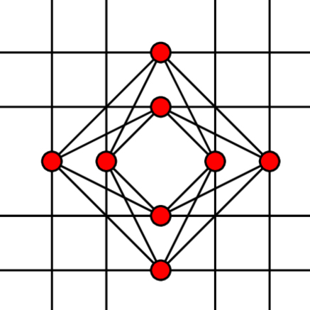
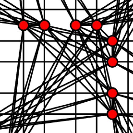
where is the initial Hamiltonian, is the (input) problem Hamiltonian, s ( [0, 1]) is a non-decreasing function of time called an annealing schedule, and L(s) are energy scaling functions of the transverse and longitudinal fields in the annealer respectively. Essentially, determines the probability of tunneling during the annealing process, and determines the probability of finding the ground state of the input problem Hamiltonian (tech, ). The QA hardware is a network of locally interacting radio-frequency superconducting qubits, organized in groups of unit cells. Fig. 3 shows the unit cell structures of recent (Chimera) and state-of-the-art (Pegasus) QA devices. The nodes and edges in the figure are qubits and couplers respectively (detailed below) (10.1145/3372224.3419207, ).
2.2. Quantum Annealing Algorithm
The process of optimizing a problem in the QA is called annealing. Starting with a high transverse field (i.e., ), QA initializes the qubits in a pre-known ground state of the initial Hamiltonian , then gradually interpolates this Hamiltonian over time—decreasing and increasing L(s)—by adiabatically introducing quantum fluctuations in a low-temperature environment, until the transverse field diminishes (i.e., ). This time-dependent interpolation of the Hamiltonian is essentially the annealing algorithm. The Adiabatic Theorem then ensures that by interpolating the Hamiltonian slowly333If the adiabatic evolution is infinitely slow, then the annealing algorithm is guaranteed to find the global minima of (smolin2014classical, ). enough, the system remains in the ground state of the interpolating Hamiltonian (baldassi2018efficiency, ). Thus during the annealing process, the system ideally stays in the local minima and probabilistically reaches the global minima of the problem Hamiltonian at its conclusion (tech, ).
The initial Hamiltonian takes the form = , where is the result of the Pauli-X matrix acting on the qubit. Thus, the initial state of the system is the ground state of this , where each qubit is in an equal superposition state . The problem Hamiltonian is described by , where is the result of the Pauli-Z matrix acting on the qubit, and are the optimization problem inputs that the user supplies (tech, ; amin2015searching, ).
Input Problem Forms. QAs optimize Ising model problems, whose problem format matches the above problem Hamiltonian: , where E is the energy of the candidate solution, is the solution variable which can take on values in {}, and are called the bias of and the coupling strength between and , respectively. Biases represent individual preferences of qubits to take on a particular classical value ( or ), whereas coupling strengths represent pairwise preferences (i.e., two particular qubits should take on same/opposite values), in the solution the machine outputs. Biases and coupling strengths are specified to qubits and couplers, respectively, using a programmable on-chip control circuitry (johnson2011quantum, ; king2018observation, ). The QA returns the solution variable configuration with the minimum energy E at its output (10.1145/3372224.3419207, ).
Assumption 1— Ising Model formulation.
To enable QA computation, cellular baseband’s heavy processing tasks must be formulated as Ising model problems. Recent prior work in this area has formulated the most heavyweight tasks in the baseband, such as frequency domain detection, forward error correction, and precoding problems, into Ising models (kim2019leveraging, ; 10.1145/3372224.3419207, ; 9500557, ; bian2014discrete, ; cui2021quantum, ). Further baseband tasks (e.g. filtering) will either admit Ising model formulations via binary representation of continuous values (aschbacher2005digital, ; mattingley2010real, ) (we leave for future work), or are so lightweight they require negligible power.
2.3. Input Problem Embedding
The process of mapping a given input problem onto the physical QA hardware is called embedding. To understand embedding, let us consider an example Ising problem:
| (2) |
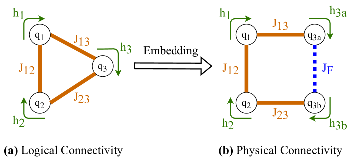
The direct/logical representation of Eq. 2 is depicted in Fig. 4(a), where nodes and edges in the figure are qubits and couplers respectively. The curved arrows in the figure are used to visualize the linear coefficients. However, observe that a complete three-node qubit connectivity does not exist in the Chimera graph (cf. Fig. 3(a)). Hence the standard approach is to map one of the logical problem variables (e.g., ) onto two physical qubits (e.g., and ) as Fig. 4(b) shows, such that the resulting connectivity can be realized on the QA hardware.
To ensure proper embedding: and must agree with each other. This is achieved by enforcing the condition , and chaining these physical qubits with a strong ferromagnetic coupling called JFerro ()—see dotted line in Fig. 4(b). The physical Ising problem the QA optimizes for the example in Eq. 2 is then:
| (3) | ||||
Assumption 2— Bespoke QA hardware
. Qubit connectivity significantly impacts performance, with sparse connectivity negatively affecting dense problem graphs due to problem mapping difficulties (10.1145/3372224.3419207, ). Recent advances in QA have bolstered qubit connectivity—6 to 15 to 20 couplers per qubit in the Chimera (2017), Pegasus (2020), and Zephyr (ca. 2023-24) topologies respectively (topologies, ; zephr, )—while further improvement efforts continue (katzgraber2018small, ; lechner2015quantum, ), which will allow QA hardware tailored to baseband processing problems within the timescales of our predictions, resulting in a highly efficient minor embedding process.
3. Quantum Processing Performance
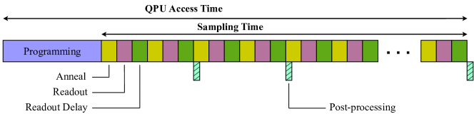
To characterize current and future QA performance, this section analyzes processing time on QA devices, the client of which sends quantum machine instructions (QMI) that characterize an input problem computation to a QA QPU. The QPU then responds with solution data. Fig. 5 depicts the the entire latency a QMI experiences from entering the QPU to the readout of the solution, which consists of programming (§3.1), sampling (§3.2), and post-processing (§3.3) times.
3.1. Programming
As the QMI reaches the QPU, the QPU programs the QMI’s input problem coefficients—biases and coupling strengths (§2): room temperature electronics send raw signals into the QA refrigeration unit to program the on-chip flux digital-to-analog converters (-DACs). The -DACs then apply external magnetic fields and magnetic couplings locally to the qubits and couplers respectively. This process is called a programming cycle, and in current technology it typically takes 4–40 s (timing, ), dictated by the bandwidth of control lines and the -DAC addressing scheme (boothby2021architectural, ). During the programming cycle, the QPU dissipates an amount of heat that increases the effective temperature of the qubits. This is due to the movement of flux quanta444QA devices store coefficient information in the form of magnetic flux quanta and it is transferred via single flux quantum (SFQ) voltage pulses (bunyk-architectural, ). in the inductive storage loops of -DACs. Thus, a post-programming thermalization time is required to cool the QPU, ensure proper reset/initialization of qubits, and allow the QPU to maintain a thermal equilibrium with the refrigeration unit (20 mK). QA clients can specify thermalization times in the range 0–10 ms with microsecond-level granularity. The default value on D-Wave’s machine is a conservative one millisecond (tech, ).
| Qubits | Couplers | -DACs | Energy, Thermalization time | |
|---|---|---|---|---|
| = 55 A (bunyk-architectural, ) | = 1 A (mcdermott2018quantum, ) | |||
| 512 | 1,472 | 4,544 | 66 fJ, 2.2 ns | 1 fJ, 33 ps |
| 2,048 | 6,016 | 18,304 | 266 fJ, 8.9 ns | 5 fJ, 167 ps |
| 5,436 | 37,440 | 70,056 | 1 pJ, 33 ns | 18 fJ, 600 ps |
| 10 M | 75 M | 135 M | 2 nJ, 66 s | 36 pJ, 1.2 s |
QMI coefficients are programmed by using six -DACs per qubit and one -DAC per coupler, and the supported bit-precision is currently up to five bits (four for value, one for sign) (bunyk-architectural, ). Each -DAC consists two inductor storage loops with a pair of Josephson junctions each. The energy dissipated on chip is on the order of per single flux quantum (SFQ) moved in an inductor storage loop, where is the -DAC’s junction critical current and is the magnetic flux quantum.555, where h is Planck’s constant and e is the electron charge. For the worst-case reprogramming scenario, this corresponds to 32 SFQs (16 to 16) moving into (or out of) all inductor storage loops of each -DAC (bunyk-architectural, ). Table 2 reports on-chip energy dissipation values for various QPU sizes and -DAC critical currents, showing that programming an example large-scale device with 10 M qubits and 75 M couplers (15 per qubit (topologies, )) will dissipate only 36 pJ on chip. With typical 30 W cooling power available at the 20 mK QPU stage (bluefors, ), this accounts for 1.2 s of QPU thermalization time.
The next step resets/initializes the qubits (cf. §2.2), during which each qubit transitions from a higher energy state to an intended ground state, generating spontaneous photon emissions, heating the QPU. Reed et al. (reed2010fast, ) demonstrate the suppression of these emissions using Purcell filters, requiring 80 ns (120 ns) for 99% (99.9%) fidelity.
An qubit, coupler, and five-bit precision QA device need to program a worst-case amount of data, which is 27 Kbytes for the current QA ( = 5,436, = 37,440) and 100 Mbytes for a large-scale QA ( = 10M, = 75M). Thus, to maintain today’s microsecond level programming cycle time in future large-scale QA, programming control lines’ bandwidth must be increased by a factor of (i.e., GHz bandwidth lines are needed). By Purcell filter design integration and sufficient amount of control line bandwidth, overall programming time (i.e., coefficient programming time + thermalization and reset) therefore reaches to 42 s in a 10M-qubit large-scale QA device.
3.2. Sampling
The process of executing a QMI on a QA device is called sampling, and the time taken for sampling is called the sampling time. The sampling time is classified into three sub-components: the anneal, readout, and readout delay times. A single QMI consists of multiple samples of an input problem, with each sample annealed and read out once, followed by a readout delay (see Fig. 5). Sampling a QMI begins after the QPU programming process.
3.2.1. Anneal.
In this time interval, the QPU implements a QA algorithm (§2.2) (tech, ) to solve the input problem, where low-frequency annealing lines control the annealing algorithm’s schedule. The bandwidth of these control lines hence limits the minimum annealing time, which is one microsecond today. Weber et al. (lincolnlab, ) propose the use of flexible print cables with a moderate bandwidth ( MHz) and high isolation ( dB) for annealing, which potentially decrease annealing time to tens of nanoseconds.
3.2.2. Readout
After annealing, the spin configuration of qubits (i.e., the solution) is read out by measuring the qubits’ persistent current () direction. This readout information propagates from the qubits to readout detectors located at the perimeter of the QPU chip via flux bias lines. Each flux bias line is a chain of electrical circuits called Quantum Flux Parametrons (QFPs), which detect and amplify qubits’ to improve the readout signal-to-noise ratio. These QFP chains act like shift registers, propagating the information from qubits to detectors (doi:10.1063/1.4939161, ). In current QA devices with qubits, there are flux bias lines, with each flux bias line responsible for reading out qubits. Further, each flux bias line reads out one qubit at a time (i.e., time-division readout), thus a total of qubits are readout in parallel. Hence, the readout time depends on the qubits’ physical locations, the bandwidth of flux bias lines, and the signal integration time. For the current status of technology, the readout time is 25–150 s per sample (tech, ). Nevertheless, recent research demonstrates promising fast readout techniques, which we describe next.
| Qubits | Qubits readout in parallel | ||
|---|---|---|---|
| Time-division | Frequency-multiplex | ||
| (doi:10.1063/1.4939161, ) | (dorche2020high, ) | ||
| 512 | 16 | 512 | 512 |
| 2,048 | 32 | 666 | 2,048 |
| 5,436 | 52 | 666 | 5,436 |
| 10 M | 2,200 | 666 | 666K |
Chen et al. (doi:10.1063/1.4764940, ) and Heinsoo et al. (PhysRevApplied.10.034040, ) describe frequency-multiplex readout schemes that enable simultaneous readout of multiple qubits within a flux bias line. While there is no fundamental limit on the number of qubits read out simultaneously, a physical limit is imposed by the line width of qubits’ readout microresonators and the 4–8 GHz operating band (6 GHz center frequency, 4 GHz bandwidth) of commercial microwave transmission line components used in the readout architecture (doi:10.1063/1.4939161, ). Microresonators with quality factor can capture line widths up to 6/ GHz, thus enabling up to 4/6 qubits to be readout simultaneously. Table 3 reports these results, showing that a of will enable up to 666 K-qubit-parallel readout. This analysis assumes that each microresonator can be fabricated at exactly its design frequency, which is currently not the case. Further developments in understanding the RF properties of microresonators will therefore be needed to achieve this multiplexing performance.
In order to avoid sample-to-sample readout correlation, microresonators reading out the current sample’s qubits must ring down before reading the next sample’s qubits. McClure et al. (PhysRevApplied.5.011001, ) achieve ring-down times on the order of hundreds of nanoseconds by applying pulse sequences that rapidly extract residual photons exiting the microresonators after readout. Fast ring down can also be achieved by switching off the QFP (after the readout) coupled to a microresonator, and then switching on a different QFP that couples the microresonator to a lossy line. While QFP on-off switching takes hundreds of nanoseconds (grover2020fast, ; 84613, ), it ensures high fidelity readout.
Recent work by Grover et al. (grover2020fast, ) show the application of QFPs as isolators, achieving a readout fidelity of 98.6% (99.6%) in 80 ns (1 s) only. Walter et al. (PhysRevApplied.7.054020, ) describe a single-shot readout scheme requiring only 48 ns (88 ns) to achieve a 98.25% (99.2%) readout fidelity. Their designs are also compatible with multiplexed architectures and earlier readout schemes, implying that by design integration readout time reaches on the order of microseconds per sample.
3.2.3. Readout delay
After a sample’s anneal-readout process, a readout delay is added (see Fig. 5). In this time interval, qubits are reset for next sample’s anneal, and QA clients can specify times in the range 0–10 ms, and the default value is a conservative one millisecond. Nevertheless, about one microsecond is sufficient for high fidelity qubit reset (§3.1) (reed2010fast, ).
3.3. Postprocessing
This time interval is used for post-processing the solutions returned by QA for improving the solution quality (post, ). Multiple samples’ solutions are post-processed at once in parallel with the current QMI’s annealer computation, whereas the final batch of post-processing occurs in parallel with the programming of next QMI (see Fig. 5). Thus, the post-processing time does not factor into the overall processing time (timing, ).
In summary, the projected overall programming time is 42 s (programming: 4–40 s, thermalization and reset: 2 s), anneal time is one s/sample, readout time is one s/sample, and readout delay time is one s/sample. For a target sample count , total QMI run time is 42 + 3 s.
4. RAN Power Models and Cellular Targets
This section describes power modeling in RANs (§4.1), 4G/5G cellular computational targets (§4.2), and QA qubit requirement to meet this computational demand (§4.3).
| BBU Task | Reference | 4G (B/W = 20 MHz) | 5G (B/W = 200 MHz) | 5G (B/W = 400 MHz) | |||||||||
|---|---|---|---|---|---|---|---|---|---|---|---|---|---|
| = 1 | = 2 | = 4 | = 8 | = 32 | = 64 | = 128 | = 32 | = 64 | = 128 | ||||
| DPD | 0.160 | 0.320 | 0.640 | 1.280 | 51.2 | 102.4 | 204.8 | 102.4 | 204.8 | 409.6 | |||
| Filter | 0.400 | 0.800 | 1.600 | 3.200 | 128.0 | 256.0 | 512.0 | 256.0 | 512.0 | 1024.0 | |||
| FFT | 0.160 | 0.320 | 0.640 | 1.280 | 51.2 | 102.4 | 204.8 | 102.4 | 204.8 | 409.6 | |||
| FD | 0.090 | 0.180 | 0.360 | 0.720 | 28.8 | 57.6 | 115.2 | 57.6 | 115.2 | 230.4 | |||
| FD | 0.030 | 0.120 | 0.480 | 1.920 | 307.2 | 1228.8 | 4915.2 | 614.4 | 2457.6 | 9830.4 | |||
| FEC | 0.140 | 0.140 | 0.280 | 0.560 | 22.4 | 44.8 | 89.6 | 44.8 | 89.6 | 179.2 | |||
| CPRI | 0.720 | 0.720 | 1.440 | 2.880 | 115.2 | 230.4 | 460.8 | 230.4 | 460.8 | 921.6 | |||
| PCP | 0.400 | 0.800 | 1.600 | 3.200 | 12.8 | 25.6 | 51.2 | 12.8 | 25.6 | 51.2 | |||
| Total | 2.100 | 3.400 | 7.040 | 15.040 | 716.8 | 2,048.0 | 6,533.6 | 1,420.8 | 4,070.4 | 13,056.0 | |||
4.1. Power Modeling
RAN power models account for power by splitting the BS or C-RAN functionality into the components and sub-components shown in Figs. 1 and 6. This section details these components and their associated power models. We follow the developments by Desset et al. (desset2012flexible, ) and Ge et al. (ge2017energy, ).
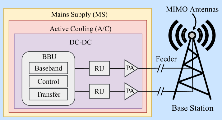
4.1.1. RAN Base Station
A RAN BS (see Fig. 6) is comprised of a baseband unit (BBU), a radio unit (RU), power amplifiers (PAs), antennas, and a power system (PS). The entire BS power consumption () is then modeled as:
| (4) |
where is the BS component’s power consumption, and , , and correspond to fractional losses of Active Cooling (A/C), Mains Supply (MS), and DC–DC conversions of the power system respectively (ge2017energy, ).
The BBU performs the processing associated with digital baseband (BB), and control and transfer systems. The baseband includes computational tasks such as digital pre-distortion (DPD), up/down sampling or filtering, OFDM-FFT processing, frequency domain (FD) mapping/demapping and equalization, and forward error correction (FEC). The control system undertakes the platform control processing (PCP), and the transfer system processes the eCPRI transport layer. The total BBU power consumption () is then (desset2012flexible, ; ge2017energy, ):
| (5) |
where is the computational task’s power consumption, and is the leakage power resulted from the employed hardware in processing these baseband tasks. FD processing is split into two parts, with linear and non-linear scaling over number of antennas (desset2012flexible, ; ge2017energy, ). The RU performs analog RF signal processing, consisting of clock generation, low-noise and variable gain amplification, IQ modulation, mixing, buffering, pre-driving, and analog–digital conversions. RU power consumption () scales linearly with number of transceiver chains, and each chain consumes about 10.8 W power (desset2012flexible, ). For macro-cell BSs, each PA (including antenna feeder) is typically configured at 102.6 W power consumption (ge2017energy, ).
4.1.2. C-RAN
In the C-RAN architecture, BS processing functionality is amortized and shared, where Remote Radio Heads (RRHs) perform analog RF signal processing and a BBU-pool performs digital baseband computation (of many BSs) at a centralized datacenter (see Fig. 1). Fronthaul (FH) links connect RRHs with the centralized BBU-pool. To relax the FH latency and bandwidth requirements, a part of baseband computation is performed at RRH sites. Several such split models have been proposed (8479363, ; 3gpp, ). We consider a split where RRHs perform low Layer 1 baseband processing, such as cyclic prefix removal and FFT-specific computation. The power consumption of C-RAN () is then:
| (6) |
where is the C-RAN component’s power consumption and is the number of RRHs. Fronthaul power consumption depends on the technology, and for fiber-based ethernet or passive optical networks, it can be modeled by assuming a set of parallel communication channels as (7437385, ; alimi2019energy, ):
| (7) |
where is a constant scaling factor, and represent the traffic load and the capacity of the fronthaul link respectively. For a link capacity of 500 Mbps, is typically ca. 37 Watts (liu2018designing, ).
4.2. Cellular Processing Requirements
This section describes 4G/5G cellular computational targets in estimated Tera operations per Second (TOPS) the BBU needs to process, and it depends on parameters such as the bandwidth (B/W), modulation (M), coding rate (R), number of antennas (), and time (dt) and frequency (df) domain duty cycles. Prior work (desset2012flexible, ; ge2017energy, ) present these TOPS complexity values for individual BBU tasks in a reference scenario (B/W = 20 MHz, M = 6, R = 1, = 1, dt = df = 100%), which we replicate in Table 4 as Reference. The scaling of these values follow (desset2012flexible, ; ge2017energy, ):
| (8) |
where X {B/W, M, R, , dt, df} and k [1,6] respectively. The scaling exponents {, , , , , } are {1,0,0,1,1,0} for DPD, Filter, and FFT, {1,0,0,1,1,1} for FD, {1,0,0,2,1,1} for FD, {1,1,1,1,1,1} for CPRI and FEC, and {0,0,0,1,0,0} for PCP (desset2012flexible, ; ge2017energy, ). These exponents are determined based on the dependence of BBU operation with the corresponding parameters (desset2012flexible, ; ge2017energy, ). Table 4 reports the TOPS complexity values for representative 4G and 5G scenarios.
4.3. QA Qubit Count Requirements
This section describes our approach in estimating the QA qubit requirement that meet the 4G/5G cellular baseband computational demand (§4.2). To compute this, we convert the target TOPS (Table 4) into target problems per second (PPS), then estimate the number of qubits QA requires to achieve this PPS, individually for baseband computational tasks. We formulate it as:
| (9) | |||
| (10) | |||
| (11) |
where is the total number of qubits the QA requires for the entire baseband processing, and is the qubit requirement for the baseband task. is the target problems per second, is the number of qubits per problem, and is the run time per problem, of the baseband task. We next demonstrate how to compute these values for and FEC tasks with running examples.
Qubit Requirement.
The task corresponds to the MIMO detection problem (albreem2019massive, ) whose objective is to demodulate the received soft symbols into bits. Solving an problem requires on average 80 (/64) million operations for a (Z-users, Z-antennas) system666A MIMO detection problem requires 80 million operations (jalden2004maximum, ), and it scales quadratic with number of antennas (desset2012flexible, ; ge2017energy, ). via state-of-the-art Sphere Decoding algorithm (jalden2004maximum, ). Solving the same problem using QA requires qubits, where is the number of bits per symbol in the modulation scheme (see (kim2019leveraging, ) for full derivation). Thus for a typical 5G scenario: MIMO system with 64-QAM modulation (i.e., six bits per symbol), is 30.72M (= 2457.6 TOPS/80M operations), is 384 qubits, and is 42 + 3 s (§3). Substituting these values in Eq. 10 shows that the 5G processing requires 1.2M qubits with samples.
FEC Qubit Requirement.
The FEC task corresponds to channel decoding that aims to correct the bit errors that interference and vagaries of the wireless channel inevitably introduce into the user data. We consider Low Density Parity Check (LDPC) codes employed in the 5G-NR traffic channel for FEC evaluation (3gppcoding, ). Decoding an (M, N)-LDPC code with average row weight and column weight in its parity check matrix via state-of-the-art belief propagation algorithm requires operations per iteration (fernandes2010parallel, ), where M and N are the number of rows and columns in the LDPC parity check matrix respectively. Solving the same problem using QA requires qubits, where —see (10.1145/3372224.3419207, ) for full derivation. Thus for the 5G’s longest LDPC code with base-graph-1 parity check matrix ( = 4224, = 8448, = 8.64, = 20) (3gpp, ), is 600K (= 89.6 TOPS/150M operations)—for typical 20 decoding iterations, is 21,120 qubits, and and is s (§3). Substituting these values in Eq. 10 shows that the 5G FEC processing requires 1.29M qubits with samples.
| : | 1 | 20 | 50 | 100 |
|---|---|---|---|---|
| 45 | 102 | 192 | 342 | |
| 530K | 1.20M | 2.26M | 4.03M | |
| : | 570K | 1.29M | 2.43M | 4.34M |
| 1.60M | 1.99M | 6.25M | 11.16M |
5G’s and FEC tasks correspond to 75% of the baseband computation load. For the remaining 25% of baseband computational load, we project a proportionate number of qubits for their respective processing requirements. Table 5 reports the number of qubits the QA requires as a function of problem run time (), showing that with of {45, 102, 192, 342} s, QA requires {1.6, 1.99, 6.25, 11.16} million qubits respectively to satisfy the 5G baseband computational demand. The number of samples () represent the required QA target fidelity in terms of error performance—when is 20, QA must reach ground state of the input problem in 20 anneals. Hence, QA must meet these and combinations to achieve spectral efficiency equal to CMOS processing in 5G wireless networks. While we demonstrate an example scenario with 400 MHz BW, 64-antennas, 64-QAM modulation, and 0.5 coding rate, a similar methodology can be applied to estimate network-specific qubit requirements. Figure 9(c) shows this qubit requirement for various bandwidths and antenna choices at 102 s problem run time.
5. Power and Cost Comparison
Our methodology compares CMOS and QA processing at equal spectral efficiency outcomes. We specify the same BBU targets (Table 4) with CMOS and QA hardware, ensuring equal bits processed per second per Hz per km2.
Power consumption of CMOS hardware depends on its performance-per-watt efficiency and the amount of computation at hand. Technology scaling improves this efficiency from generation to generation, inversely proportional to the square of its transistors’ core supply voltage () (stillmaker2017scaling, ). A 65 nm CMOS device ( = 1.1 V) has a 0.04 TOPS/Watt efficiency, from which we compute the same for today’s 14 nm CMOS ( = 0.8 V) and future 1.5 nm CMOS ( = 0.4 V), via scaling, and they obtain a 0.076 and 0.3 TOPS/Watt efficiency respectively (desset2012flexible, ; itrs, ; itrs_old, ). Using this hardware efficiency and the TOPS requirements of Table 4, we compute CMOS hardware power consumption. Additional power results from leakage currents in CMOS transistor channel, and this leakage power is set to 30% of dynamic power (desset2012flexible, ).
Power consumption of D-Wave’s QA is ca. 25 kW, dominated by its refrigeration unit (see Supplementary information–(king-naturecomms2021, )). Additional power draw due to the computation at hand is fairly negligible compared to the QA refrigeration power, since the QPU resources used for computation are thermally isolated in a superconducting environment. This power requirement is further not expected to significantly scale up with increased qubit numbers (villalonga2020establishing, ; king-naturecomms2021, ), due to the fairly constant power consumption of pulse-tube dilution refrigerators which are used to cool the QPU in practice (nextdwave, ; king-naturecomms2021, ; bluefors, ). More general NISQ processors such as Google’s Sycamore (see Supplementary information–(google-nature19, )) and IBM’s Rochester (ibmrochester, ) also show a similar ca. 25 kW power consumption and a fairly constant scaling with increased qubit numbers (villalonga2020establishing, ). However, to maintain this 25 kW power for the entire 5G baseband processing, sufficient amount of qubits are required, all under the same refrigeration unit. This raises the question—how many qubits are allowed in a QA refrigeration unit?
To answer this question, we consider the physical size of qubits in their unit cell packaging (a die) versus the available space in the dilution refrigerator. The number of useful square dies () of length placed onto a wafer of radius is approximately (de2005investigation, ): . A square die of eight qubits requires 335335 QPU chip area with = 335 m (bunyk-architectural, ), and a dilution refrigerator’s experimental space has a radius = 250 mm (bluefors, ). Substituting these values in the above equation gives 1.75M, which implies 14 million qubits allowed in a refrigeration unit. Since qubit count estimates for 5G (cf. §4.3, §6) are well below this allowed limit, QA power consumption is 25 kW for 5G baseband processing.
Results and discussion:
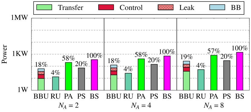
Applying the foregoing power analysis, Fig. 7 reports power consumption results of 4G and 5G BSs with 14 nm CMOS hardware. In Fig. 7(a), we see that the power amplifier (PA) is the dominating component of 4G BS power consumption, as identified in several prior works (desset2012flexible, ; ge2017energy, ; alimi2019energy, ), accounting for 57–58% of the total BS power. But, as the network scales to higher bandwidth and antennas envisioned in 5G, the BBU becomes the dominant power consuming component (see Fig. 7(b)), accounting for 69–74% of the total BS power. This quick escalation in power from 0.35–1.43 kW in 4G to 34.7–261.3 kW in 5G is mainly due to the quadratic dependency of FD processing with number of antennas (§4.1), and the increased network bandwidth consequence of millimeter-wave communication.
Fig. 8(a) reports the power consumption results of 5G BS, where QA is used for BBU’s baseband processing. In comparison to CMOS–Fig. 7(b), QA reduces BS power by 41 kW and 188 kW in 64 and 128 antenna systems. Fig. 8(b) shows power consumption in a C-RAN setting with three 64-antenna BSs, where the fronthaul is allowed a 100 Gbps bandwidth. In comparison to CMOS, QA processing reduces C-RAN power by 159 kW (55% lower). Table 6 reports the OpEx cost savings and carbon emission reductions associated with the respective power savings, computed by considering an average $0.143 (USD) electricity price and 0.92 pounds of equivalent emitted per kWh (blscost, ; carbon, ). To provide economic benefit over CMOS hardware, assuming CMOS CapEx is negligible, future QAs’ CapEx must be lower than the respective OpEx savings. For instance, if QA was to be employed in a C-RAN scenario, a CapEx lower than 200K, 400K, 1M, and 2M USD will provide economic benefit over CMOS in one, two, five, and 10 years, respectively.
| Years | BS ( = 64) | BS ( = 128) | C-RAN | |||
|---|---|---|---|---|---|---|
| Cost ($) | (kt) | Cost | Cost | |||
| 1 | 50K | 0.15 | 235K | 0.68 | 200K | 0.57 |
| 2 | 100K | 0.30 | 471K | 1.37 | 400K | 1.15 |
| 5 | 250K | 0.75 | 1.17M | 3.43 | 1M | 2.87 |
| 10 | 500K | 1.50 | 2.35M | 6.87 | 2M | 5.75 |
6. Feasibility Timeline and Discussion
This section presents our projected QA feasibility timeline, describing year-by-year milestones on the application of QA to wireless networks. Our approach is to compare power consumption of QA and CMOS in various base station scenarios, then compute the QA qubit requirement to equal spectral efficiency to CMOS in the same scenarios. We next project the year by which these qubit numbers become available in the QA hardware by extrapolating the historical QA qubit growth trend into future. Figures 2 and 9 report these results.
Roadmap for feasibility. The processing of a base station with 10-MHz bandwidth and 32 antennas (Point ‘F’ in Fig. 9(c)) requires 39K qubits in the QA hardware for QA to equal spectral efficiency to CMOS, and this qubit requirement is projected to become available by the year 2026 (Figs. 2, 9(c)). However, leveraging QA for such a system leads to increased power consumption in comparison to both 14 nm and 1.5 nm CMOS devices (Figs. 9(a), 9(b)).
Roadmap for Power dominance. From Figs. 9(a) and 9(b), we see that for a given antenna count, the lowest bandwidth for which QA achieves power advantage over 14 nm CMOS are 20 MHz bandwidth 256-antenna (Point ‘A’), 50 MHz bandwidth 128-antenna (Point ‘B’), and 160 MHz bandwidth 64-antenna (Point ‘C’) systems. In comparison to 1.5 nm CMOS, such points correspond to 60 MHz bandwidth 256-antenna (Point ‘D’), and 190 MHz bandwidth 128-antenna (Point ‘E’) systems. Fig. 9(c) shows the number of qubits required in the QA hardware to process these systems (Points A–E) with equal spectral efficiency to CMOS. The figure shows that to achieve a power dominance over 14 nm CMOS, at least 618K qubits (Point ‘A’) are required in the QA hardware, and this qubit requirement is projected to become available by the year 2035 (Figs. 2, 9(c)). QA with at least 1.85M qubits benefit in power over 1.5 nm CMOS, and such a QA is predicted to become available by the year 2038 (Figs. 2, 9(c)). In summary, our analyses show that power advantage of QA over CMOS is a predicted 14–17 years away. Fig. 2 summarizes Fig. 9 in a feasibility timeline, showing the years by which QA enables these base station operation scenarios along with their associated power advantage/loss.
7. Conclusion
While the conventional assumption that CMOS hardware will achieve nextG cellular processing targets may well hold true, this paper makes the case for the possible future feasibility and potential power advantage of QA over CMOS. Our extensive analysis of current QA technology projects quantitative targets that future QAs may well meet in order to provide benefits over CMOS in terms of performance, power, and cost. While we acknowledge the practical deployment of quantum processors to be at least tens of years away, this early study informs future quantum hardware design and RAN architecture evolution. Furthermore, fundamental physical advances in the QA technology itself, which we do not leverage in the projections given in this paper, may offer even further benefits, advantaging our projected timelines. Examples of these advances include faster annealing times ( ns) and/or qubits with longer coherence lifetimes (such as the qubits in IARPA’s QEO and DARPA’s QAFS QA chips (darpa, )) that enable coherent quantum annealing regimes, benefiting future QA spectral efficiency (fastanneal, ; yan2016flux, ).
Acknowledgements
This research is supported by National Science Foundation (NSF) Award CNS-1824357. We thank Andrew J. Berkley, Keith Briggs, Andrew D. King, Catherine McGeoch, Davide Venturelli, and Catherine White for useful discussions. P.A.W. is supported by the Engineering and Physical Sciences Research Council (EPSRC) Hub in Quantum Computing and Simulation, Grant Ref. EP/T001062/1.
References
- (1) M. Agiwal, A. Roy, N. Saxena. Next Generation 5G Wireless Networks: A Comprehensive Survey. IEEE Communications Surveys Tutorials, 18(3), 1617–1655, 2016. doi:10.1109/COMST.2016.2532458.
- (2) M. A. Albreem, M. Juntti, S. Shahabuddin. Massive mimo detection techniques: A survey. IEEE Communications Surveys & Tutorials, 21(4), 3109–3132, 2019.
- (3) I. A. Alimi, A. M. Abdalla, A. Olapade Mufutau, F. Pereira Guiomar, I. Otung, J. Rodriguez, P. Pereira Monteiro, A. L. Teixeira. Energy efficiency in the cloud radio access network (C-RAN) for 5G mobile networks: Opportunities and challenges. Optical and Wireless Convergence for 5G Networks, 225–248, 2019.
- (4) M. H. Amin. Searching for quantum speedup in quasistatic quantum annealers. Physical Review A, 92(5), 052,323, 2015.
- (5) F. Arute, K. Arya, R. Babbush, D. Bacon, J. C. Bardin, R. Barends, R. Biswas, S. Boixo, F. G. S. L. Brandao, D. A. Buell, B. Burkett, Y. Chen, Z. Chen, B. Chiaro, R. Collins, W. Courtney, A. Dunsworth, E. Farhi, B. Foxen, A. Fowler, C. Gidney, M. Giustina, R. Graff, K. Guerin, S. Habegger, M. P. Harrigan, M. J. Hartmann, A. Ho, M. Hoffmann, T. Huang, T. S. Humble, S. V. Isakov, E. Jeffrey, Z. Jiang, D. Kafri, K. Kechedzhi, J. Kelly, P. V. Klimov, S. Knysh, A. Korotkov, F. Kostritsa, D. Landhuis, M. Lindmark, E. Lucero, D. Lyakh, S. Mandrà, J. R. McClean, M. McEwen, A. Megrant, X. Mi, K. Michielsen, M. Mohseni, J. Mutus, O. Naaman, M. Neeley, C. Neill, M. Y. Niu, E. Ostby, A. Petukhov, J. C. Platt, C. Quintana, E. G. Rieffel, P. Roushan, N. C. Rubin, D. Sank, K. J. Satzinger, V. Smelyanskiy, K. J. Sung, M. D. Trevithick, A. Vainsencher, B. Villalonga, T. White, Z. J. Yao, P. Yeh, A. Zalcman, H. Neven, J. M. Martinis. Quantum supremacy using a programmable superconducting processor. Nature, 574(7779), 505–510, 2019. doi:10.1038/s41586-019-1666-5.
- (6) E. Aschbacher. Digital pre-distortion of microwave power amplifiers. Ph.D. thesis, 2005.
- (7) C. Baldassi, R. Zecchina. Efficiency of quantum versus classical annealing in non-convex learning problems. Proceedings of the National Academy of Sciences, 115(7), 1457–1462, 2018.
- (8) Z. Bian, F. Chudak, R. Israel, B. Lackey, W. G. Macready, A. Roy. Discrete optimization using quantum annealing on sparse ising models. Frontiers in Physics, 2, 56, 2014.
- (9) BlueFors. BlueFors XLD1000 Dilution Refrigerator System, Website.
- (10) S. Boixo, T. F. Rønnow, S. V. Isakov, Z. Wang, D. Wecker, D. A. Lidar, J. M. Martinis, M. Troyer. Quantum annealing with more than one hundred qubits. arXiv preprint arXiv:1304.4595, 2013.
- (11) K. Boothby, C. Enderud, T. Lanting, R. Molavi, N. Tsai, M. H. Volkmann, F. Altomare, M. H. Amin, M. Babcock, A. J. Berkley, et al. Architectural considerations in the design of a third-generation superconducting quantum annealing processor. arXiv preprint arXiv:2108.02322, 2021.
- (12) P. I. Bunyk, E. M. Hoskinson, M. W. Johnson, E. Tolkacheva, F. Altomare, A. J. Berkley, R. Harris, J. P. Hilton, T. Lanting, A. J. Przybysz, J. Whittaker. Architectural considerations in the design of a superconducting quantum annealing processor. IEEE Transactions on Applied Superconductivity, 24(4), 1–10, 2014. doi:10.1109/TASC.2014.2318294.
- (13) Y. Cao, Y. Zhao, F. Dai. Node localization in wireless sensor networks based on quantum annealing algorithm and edge computing. 2019 International Conference on Internet of Things (iThings) and IEEE Green Computing and Communications (GreenCom) and IEEE Cyber, Physical and Social Computing (CPSCom) and IEEE Smart Data (SmartData), 564–568. IEEE, 2019.
- (14) N. Chancellor, S. Zohren, P. A. Warburton, S. C. Benjamin, S. Roberts. A direct mapping of max k-SAT and high order parity checks to a chimera graph. Scientific reports, 6(1), 1–9, 2016.
- (15) A. Checko, H. L. Christiansen, Y. Yan, L. Scolari, G. Kardaras, M. S. Berger, L. Dittmann. Cloud RAN for mobile networks—a technology overview. IEEE Communications surveys & tutorials, 17(1), 405–426, 2014.
- (16) Y. Chen, D. Sank, P. O’Malley, T. White, R. Barends, B. Chiaro, J. Kelly, E. Lucero, M. Mariantoni, A. Megrant, C. Neill, A. Vainsencher, J. Wenner, Y. Yin, A. N. Cleland, J. M. Martinis. Multiplexed dispersive readout of superconducting phase qubits. Applied Physics Letters, 101(18), 182,601, 2012. doi:10.1063/1.4764940.
- (17) Cisco. Annual Internet Report (2018–2023) White Paper, 2018.
- (18) R. Courtland. Transistors could stop shrinking in 2021. IEEE Spectrum, 53(9), 9–11, 2016.
- (19) J. Cui, Y. Xiong, S. X. Ng, L. Hanzo. Quantum approximate optimization algorithm based maximum likelihood detection. arXiv preprint arXiv:2107.05020, 2021.
- (20) D-Wave Systems User Manual. Postprocessing Methods on D-Wave Systems, 2021.
- (21) D-Wave Next Generation Plans and Activities, 2018.
- (22) D-Wave Systems User Manual. Solver Computation Time, 2021.
- (23) D-Wave Systems User Manual. Technical Description of the D-Wave Quantum Processing Unit, 2021.
- (24) D-Wave Systems. Clarity: A roadmap for the future of quantum computing, 2021.
- (25) D-Wave Systems. D-Wave QPU Architecture: Topologies, Website.
- (26) D-Wave Systems. Zephyr Topology of D-Wave Quantum Processors, Website.
- (27) B. Dai, W. Yu. Energy efficiency of downlink transmission strategies for cloud radio access networks. IEEE Journal on Selected Areas in Communications, 34(4), 1037–1050, 2016. doi:10.1109/JSAC.2016.2544459.
- (28) D. K. De Vries. Investigation of gross die per wafer formulas. IEEE Transactions on Semiconductor Manufacturing, 18(1), 136–139, 2005.
- (29) C. Desset, B. Debaillie, V. Giannini, A. Fehske, G. Auer, H. Holtkamp, W. Wajda, D. Sabella, F. Richter, M. J. Gonzalez, et al. Flexible power modeling of LTE base stations. 2012 IEEE wireless communications and networking conference (WCNC), 2858–2862. IEEE, 2012.
- (30) A. E. Dorche, B. Wei, C. Raman, A. Adibi. High-quality-factor microring resonator for strong atom–light interactions using miniature atomic beams. Opt. Lett., 45(21), 5958–5961, 2020. doi:10.1364/OL.404331.
- (31) G. F. P. Fernandes. Parallel algorithms and architectures for LDPC Decoding. Ph.D. thesis, 2010.
- (32) X. Ge, J. Yang, H. Gharavi, Y. Sun. Energy efficiency challenges of 5G small cell networks. IEEE Communications Magazine, 55(5), 184–191, 2017. doi:10.1109/MCOM.2017.1600788.
- (33) 3rd Generation Partnership Project (3GPP). Study on new radio access technology: Radio access architecture and interfaces, TS 38.801, v.14.0.0, 2017.
- (34) 3rd Generation Partnership Project (3GPP). Technical specification group services and system aspects, TR 21.915, v.15.0.0, 2017.
- (35) 3rd Generation Partnership Project (3GPP). Multiplexing and channel coding. TS 38.212, v.15.3.0, 2018.
- (36) J. A. Grover, J. I. Basham, A. Marakov, S. M. Disseler, R. T. Hinkey, M. Khalil, Z. A. Stegen, T. Chamberlin, W. DeGottardi, D. J. Clarke, et al. Fast, lifetime-preserving readout for high-coherence quantum annealers. PRX Quantum, 1(2), 020,314, 2020.
- (37) R. Harris. Outrunning the bear: Quantum annealing in the presence of an environment. Adiabatic Quantum Computing Conference (AQC), 2021.
- (38) J. Heinsoo, C. K. Andersen, A. Remm, S. Krinner, T. Walter, Y. Salathé, S. Gasparinetti, J.-C. Besse, A. Potočnik, A. Wallraff, C. Eichler. Rapid high-fidelity multiplexed readout of superconducting qubits. Phys. Rev. Applied, 10, 034,040, 2018. doi:10.1103/PhysRevApplied.10.034040.
- (39) M. Hosoya, W. Hioe, J. Casas, R. Kamikawai, Y. Harada, Y. Wada, H. Nakane, R. Suda, E. Goto. Quantum flux parametron: a single quantum flux device for josephson supercomputer. IEEE Transactions on Applied Superconductivity, 1(2), 77–89, 1991. doi:10.1109/77.84613.
- (40) IBM. Quantum computation center opens, IBM research blog, 2019.
- (41) IBM. Quantum computing systems, Website.
- (42) F. Ishizaki. Computational method using quantum annealing for TDMA scheduling problem in wireless sensor networks. 2019 13th International Conference on Signal Processing and Communication Systems (ICSPCS), 1–9. IEEE, 2019.
- (43) ITRS. International technology roadmap for semiconductors, executive report, 2003.
- (44) ITRS. International technology roadmap for semiconductors 2.0, executive report, 2015.
- (45) J. Jalden. Maximum likelihood detection for the linear MIMO channel. Ph.D. thesis, 2004.
- (46) M. W. Johnson, M. H. Amin, S. Gildert, T. Lanting, F. Hamze, N. Dickson, R. Harris, A. J. Berkley, J. Johansson, P. Bunyk, et al. Quantum annealing with manufactured spins. Nature, 473(7346), 194–198, 2011.
- (47) S. Kasi, K. Jamieson. Towards quantum belief propagation for LDPC decoding in wireless networks. Proceedings of the 26th Annual International Conference on Mobile Computing and Networking, MobiCom ’20. Association for Computing Machinery, New York, NY, USA, 2020. ISBN 9781450370851. doi:10.1145/3372224.3419207.
- (48) S. Kasi, A. K. Singh, D. Venturelli, K. Jamieson. Quantum annealing for large MIMO downlink vector perturbation precoding. ICC 2021 - IEEE International Conference on Communications, 1–6, 2021. doi:10.1109/ICC42927.2021.9500557.
- (49) H. G. Katzgraber, M. Novotny. How small-world interactions can lead to improved quantum annealer designs. Physical Review Applied, 10(5), 054,004, 2018.
- (50) H. N. Khan, D. A. Hounshell, E. R. Fuchs. Science and research policy at the end of moore’s law. Nature Electronics, 1(1), 14–21, 2018.
- (51) M. Kim, D. Venturelli, K. Jamieson. Leveraging quantum annealing for large MIMO processing in centralized radio access networks. Proceedings of the ACM Special Interest Group on Data Communication, SIGCOMM ’19, 241–255. Association for Computing Machinery, New York, NY, USA, 2019. ISBN 9781450359566. doi:10.1145/3341302.3342072.
- (52) A. D. King, J. Carrasquilla, J. Raymond, I. Ozfidan, E. Andriyash, A. Berkley, M. Reis, T. Lanting, R. Harris, F. Altomare, et al. Observation of topological phenomena in a programmable lattice of 1,800 qubits. Nature, 560(7719), 456–460, 2018.
- (53) A. D. King, J. Raymond, T. Lanting, S. V. Isakov, M. Mohseni, G. Poulin-Lamarre, S. Ejtemaee, W. Bernoudy, I. Ozfidan, A. Y. Smirnov, M. Reis, F. Altomare, M. Babcock, C. Baron, A. J. Berkley, K. Boothby, P. I. Bunyk, H. Christiani, C. Enderud, B. Evert, R. Harris, E. Hoskinson, S. Huang, K. Jooya, A. Khodabandelou, N. Ladizinsky, R. Li, P. A. Lott, A. J. R. MacDonald, D. Marsden, G. Marsden, T. Medina, R. Molavi, R. Neufeld, M. Norouzpour, T. Oh, I. Pavlov, I. Perminov, T. Prescott, C. Rich, Y. Sato, B. Sheldan, G. Sterling, L. J. Swenson, N. Tsai, M. H. Volkmann, J. D. Whittaker, W. Wilkinson, J. Yao, H. Neven, J. P. Hilton, E. Ladizinsky, M. W. Johnson, M. H. Amin. Scaling advantage over path-integral monte carlo in quantum simulation of geometrically frustrated magnets. Nature Communications, 12(1), 1113, 2021. doi:10.1038/s41467-021-20901-5.
- (54) E. Knill. Quantum computing with realistically noisy devices. Nature, 434(7029), 39–44, 2005.
- (55) B. Lackey. A belief propagation algorithm based on domain decomposition. arXiv preprint arXiv:1810.10005, 2018.
- (56) P. Lähdekorpi, M. Hronec, P. Jolma, J. Moilanen. Energy efficiency of 5G mobile networks with base station sleep modes. 2017 IEEE Conference on Standards for Communications and Networking (CSCN), 163–168. IEEE, 2017.
- (57) L. M. P. Larsen, A. Checko, H. L. Christiansen. A survey of the functional splits proposed for 5G mobile crosshaul networks. IEEE Communications Surveys Tutorials, 21(1), 146–172, 2019. doi:10.1109/COMST.2018.2868805.
- (58) W. Lechner, P. Hauke, P. Zoller. A quantum annealing architecture with all-to-all connectivity from local interactions. Science advances, 1(9), e1500,838, 2015.
- (59) D. Lidar. Achievements of the IARPA-QEO and DARPA-QAFS programs & The prospects for quantum enhancement with QA, Adiabatic Quantum Computing Conference 2021 (AQC 2021).
- (60) Q. Liu, T. Han, N. Ansari, G. Wu. On designing energy-efficient heterogeneous cloud radio access networks. IEEE Transactions on Green Communications and Networking, 2(3), 721–734, 2018.
- (61) J. Mattingley, S. Boyd. Real-time convex optimization in signal processing. IEEE Signal processing magazine, 27(3), 50–61, 2010.
- (62) D. T. McClure, H. Paik, L. S. Bishop, M. Steffen, J. M. Chow, J. M. Gambetta. Rapid driven reset of a qubit readout resonator. Phys. Rev. Applied, 5, 011,001, 2016. doi:10.1103/PhysRevApplied.5.011001.
- (63) R. McDermott, M. Vavilov, B. Plourde, F. Wilhelm, P. Liebermann, O. Mukhanov, T. Ohki. Quantum–classical interface based on single flux quantum digital logic. Quantum science and technology, 3(2), 024,004, 2018.
- (64) Nokia. Mobile data growth and 5G… Are we getting the numbers right?, 2018.
- (65) J. Preskill. Fault-tolerant quantum computation. Introduction to quantum computation and information, 213–269. World Scientific, 1998.
- (66) J. Preskill. Quantum computing in the NISQ era and beyond. Quantum, 2, 79, 2018.
- (67) M. D. Reed, B. R. Johnson, A. A. Houck, L. DiCarlo, J. M. Chow, D. I. Schuster, L. Frunzio, R. J. Schoelkopf. Fast reset and suppressing spontaneous emission of a superconducting qubit. Applied Physics Letters, 96(20), 203,110, 2010.
- (68) J. Shalf. The future of computing beyond moore’s law. Philosophical Transactions of the Royal Society A, 378(2166), 20190,061, 2020.
- (69) P. W. Shor. Fault-tolerant quantum computation. Proceedings of 37th Conference on Foundations of Computer Science, 56–65. IEEE, 1996.
- (70) J. A. Smolin, G. Smith. Classical signature of quantum annealing. Frontiers in physics, 2, 52, 2014.
- (71) A. Stillmaker, B. Baas. Scaling equations for the accurate prediction of CMOS device performance from 180 nm to 7 nm. Integration, 58, 74–81, 2017.
- (72) U.S. Bureau of Labor Statistics. Average energy prices for the united states, regions, census divisions, and selected metropolitan areas, 2021.
- (73) U.S. Energy Information Administration. How much carbon dioxide is produced per kilowatthour of U.S. electricity generation?, 2019.
- (74) E. Vahapoglu, J. P. Slack-Smith, R. C. Leon, W. H. Lim, F. E. Hudson, T. Day, T. Tanttu, C. H. Yang, A. Laucht, A. S. Dzurak, et al. Single-electron spin resonance in a nanoelectronic device using a global field. Science Advances, 7(33), eabg9158, 2021.
- (75) B. Villalonga, D. Lyakh, S. Boixo, H. Neven, T. S. Humble, R. Biswas, E. G. Rieffel, A. Ho, S. Mandrà. Establishing the quantum supremacy frontier with a 281 pflop/s simulation. Quantum Science and Technology, 5(3), 034,003, 2020.
- (76) T. Walter, P. Kurpiers, S. Gasparinetti, P. Magnard, A. Potočnik, Y. Salathé, M. Pechal, M. Mondal, M. Oppliger, C. Eichler, A. Wallraff. Rapid high-fidelity single-shot dispersive readout of superconducting qubits. Phys. Rev. Applied, 7, 054,020, 2017. doi:10.1103/PhysRevApplied.7.054020.
- (77) C. Wang, H. Chen, E. Jonckheere. Quantum versus simulated annealing in wireless interference network optimization. Scientific reports, 6(1), 1–9, 2016.
- (78) C. Wang, E. Jonckheere. Simulated versus reduced noise quantum annealing in maximum independent set solution to wireless network scheduling. Quantum Information Processing, 18(1), 1–25, 2019.
- (79) S. Weber, J. Cummings, J. Miloshi, K. J. Thompson, J. Rokosz, D. Holtman, D. Conway, A. Kerman, W. D. Oliver. High-density I/O for next-generation quantum annealing: Part 1—Cryogenic wiring. APS March Meeting, 2021.
- (80) J. D. Whittaker, L. J. Swenson, M. H. Volkmann, P. Spear, F. Altomare, A. J. Berkley, B. Bumble, P. Bunyk, P. K. Day, B. H. Eom, R. Harris, J. P. Hilton, E. Hoskinson, M. W. Johnson, A. Kleinsasser, E. Ladizinsky, T. Lanting, T. Oh, I. Perminov, E. Tolkacheva, J. Yao. A frequency and sensitivity tunable microresonator array for high-speed quantum processor readout. Journal of Applied Physics, 119(1), 014,506, 2016. doi:10.1063/1.4939161.
- (81) A. Wichert. Principles of quantum artificial intelligence: quantum problem solving and machine learning. World Scientific, 2020.
- (82) J. Wu, Y. Zhang, M. Zukerman, E. K.-N. Yung. Energy-efficient base-stations sleep-mode techniques in green cellular networks: A survey. IEEE communications surveys & tutorials, 17(2), 803–826, 2015.
- (83) F. Yan, S. Gustavsson, A. Kamal, J. Birenbaum, A. P. Sears, D. Hover, T. J. Gudmundsen, D. Rosenberg, G. Samach, S. Weber, et al. The flux qubit revisited to enhance coherence and reproducibility. Nature communications, 7(1), 1–9, 2016.