Strain-controlled Domain Wall injection into nanowires for sensor applications
Abstract
We investigate experimentally the effects of externally applied strain on the injection of 180∘ domain walls (DW) from a nucleation pad into magnetic nanowires, as typically used for DW-based sensors. In our study the strain, generated by substrate bending, induces in the material a uniaxial anisotropy due to magnetoelastic coupling. To compare the strain effects, , and samples with in-plane magnetization and different magnetoelastic coupling are deposited. In these samples, we measure the magnetic field required for the injection of a DW, by imaging differential contrast in a magneto-optical Kerr microscope. We find that strain increases the DW injection field, however, the switching mechanism depends strongly on the direction of the strain with respect to the wire axis. We observe that low magnetic anisotropy facilitates the creation of a domain wall at the junction between the pad and the wire, whereas a strain-induced magnetic easy axis significantly increases the coercive field of the nucleation pad. Additionally, we find that the effects of mechanical strain can be counteracted by a magnetic uniaxial anisotropy perpendicular to the strain-induced easy axis. In , we show that this anisotropy can be induced by annealing in a magnetic field. We perform micromagnetic simulations to support the interpretation of our experimental findings. Our simulations show that the above described observations can be explained by the effective anisotropy in the device. The anisotropy influences the switching mechanism in the nucleation pad as well as the pinning of the DW at the wire entrance. As the DW injection is a key operation for sensor performances, the observations show that strain is imposing a lower limit for the sensor field operating window.
I Introduction
Domain walls (DWs) have always been of importance for their static and dynamic properties since the use of magnetic materials for logic devices and data storageKläui (2008); Spain (1966). In the last 15 years, the possibility to realize and characterize magnetic nanostructures has allowed one to explore complex spin textures, their creation and stability. This intense research has enabled the use of DWs in memory devicesParkin, Hayashi, and Thomas (2008) and magnetic sensorsJogschies et al. (2015). For example, a DW can be used to carry information about the angular position of an object and to count the number of rotations performed in a non-volatile wayDiegel, Mattheis, and Halder (2007); Mattheis et al. (2012); Borie et al. (2017a). The interest of magnetic sensors based on DWs is in their stability, making their non-volatile positioning suitable to many applications. No external electrical power is required to manipulate the magnetic state in the sensor, making it ideal for energy efficient systems even where power failures can occur.
The magnetic field conditions under which a DW based sensor can reliably operate are called field operating windowBorie et al. (2017b). For the sensor to work, a DW needs to be successfully created and propagated into the nanowire, setting the minimum operation field value. At the same time, uncontrolled nucleation of domain walls at higher fields needs to be avoided, thus setting the maximum operation field value. Previous studies about DW sensors investigated the propagation and nucleation fields, and showed how they depend on material parameters and device geometry Martinez et al. (2007, 2009); Garcia-Sanchez et al. (2011); Borie et al. (2017b, a); Hoang et al. (2020). While the field operation window in idealized operation conditions is known, in real devices further factors play a role and have been previously neglected.
Among the external factors, strain or mechanical stress on these sensing elements is known to be a key issue. Such strain occurs during packaging as well as sensor operation, with strong impact on the device performanceVan Driel et al. (2003). Strain in magnetic materials is known to induce a preferential direction of magnetization (anisotropy) due to magnetoelastic coupling Lee (1955); Finizio et al. (2014) and even pin a DW in a nanowireLei et al. (2013). In DW based devices, a common approach to generate a DW is to use a larger magnetic (nucleation) pad attached to the nanowire exploiting the reduced shape anisotropyCowburn et al. (2002); Shigeto, Shinjo, and Ono (1999); Hoang et al. (2020) as shown in figure 1. It has been shown recently using simulations how, in the nucleation pad, strain-induced anisotropy can overcome the shape anisotropy governing the switching of the magnetic state Zhou et al. (2020). However, these previous studies did not report experiments on strain effects in a sensor relevant system as ours.
In the work presented here, we investigate experimentally the impact of externally applied strain on the injection of a 180∘ domain wall from a nucleation pad in a magnetic nanowire. We employ magneto-optical Kerr effect (MOKE) microscopy to image the DW creation, pinning and injection from the pad for different external strain configurations. The injection field is strongly affected by the effective anisotropy of the magnetic material, which is modified by strain. Simulations are used to identify the switching mechanism and the spin structure of a pinned DW just before the injection into the wire.
II Experimental methods
We investigate three different samples: , and , all layers are deposited by magnetron sputtering. The substrate is thick, thermally oxidized on top of 625 undoped . To improve amorphisation and deposition uniformity, the magnetic material was sputtered in a rotating magnetic field of . The result is a soft magnetic material with intrinsically low anisotropy field and low coercive field. The magnetic properties of our films, as deposited, are summarized in table 1. For the characterization of our material we used a BH-Looper, an hysteresis loop tracer, where B is the measured magnetic flux and H is the applied magnetic field (Shb Instruments - Model 109). This tool includes a setup for measuring magnetostrictionChoe and Megdal (1999); Hill et al. (2013); Raghunathan, Snyder, and Jiles (2009).
| Material | x | |||
|---|---|---|---|---|
| 1.40(5) | 0.20(5) | 0.10(5) | 27(1) | |
| 0.95(5) | 0.10(5) | 0.10(5) | -0.5(1) | |
| 0.60(5) | 2.00(5) | 2.00(5) | -32(1)Cullity and Graham (2011) |
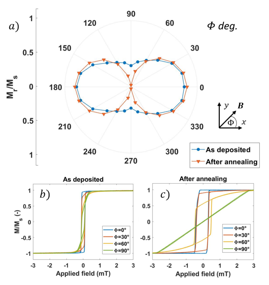
To induce a preferential direction of magnetization in the , the sample was annealed in for 2 hours at , while a static field of is applied. This treatment induces a uniaxial anisotropyZhang et al. (2011), where the easy axis of the magnetization is in the direction of the applied magnetic field. The anisotropy field after annealing is and the uniaxial anisotropy constant is , where is the saturation magnetization of the magnetic material. A comparison of the angular dependence of the remanent magnetization and hysteresis loops before and after annealing are shown for , respectively in figure 2 a) and b) - c). The structures are then patterned using photolithograpy and Ar ion milling.
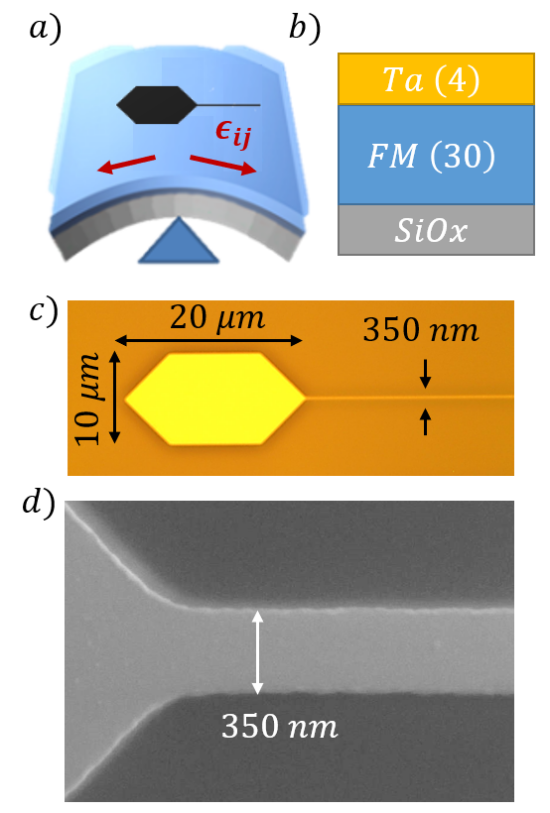
The devices used in this study can be seen in figure 1 c). A nucleation pad ( ) is attached to a long nanowire with different widths, from to . The specific geometry of the pad is designed to narrow the field distribution for injecting magnetic domains into the wire, and to allow for a DW nucleation at low fields.
To switch the magnetization in the device, we applied an external in-plane magnetic field in the direction (aligned with the nanowire). As the magnitude of the field is increased, the nucleated DW depins from the pad and is injected into the nanowire (injection field, ). We measure the injection field by imaging differential contrast changes in the magneto-optical Kerr effect (MOKE) in a longitudinal configuration of the polarized white light. To image and detect the switching event, a 50x magnification objective was used. The magnetic contrast, without structural contrast, is accomplished by subtracting a reference image in the saturated stage, at the beginning of the measurement. We have conducted our experiment at fields lower than the spontaneous domain nucleation field in the wire, that is reported to be around Borie et al. (2017b). This ensures us that a DW is injected from the pad into the wire, and not from structure defects or nucleated at the edge of the wire.
To apply strain to our devices, the substrate was bent mechanically with a sample holder that applies an out of plane force as shown schematically in figure 1 a). A square sample of 1 by 1 cm is clamped on two sides and pushed by a cylinder uniformly from below. The device generates a tensile strain in the plane of the sample up to . The strain is mostly uniaxialRaghunathan, Snyder, and Jiles (2009) and uniform in the central area of the sample, and thus in the measured area. The intensity of the strain induced on the surface of the has been measured with a strain gauge (RS PRO). The stack is thin enough to assume that the strain is entirely transferred to our device and that shear strain is negligibleThomas et al. (2003).
III Results and discussion
III.1 Injection field in nanowires
The injection field is the minimum field required to create and propagate a DW in the magnetic sensor device. However, to obtain reliable and a repeatable injection, one needs to understand the whole process of the DW injection. The MOKE images allow us to observe how the magnetization is gradually switched in the nucleation pad, creating a DW at its end, and also, captures the moment when a DW starts propagating into the wire.
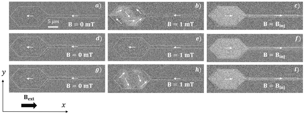
In the absence of strain, the domain configuration in the pad is mostly dominated by the shape anisotropy, and is not varying strongly for the materials studied. We indeed obtain similar images for all the measured devices. The process of injection can be observed in figure 3 a) - c). When no strain is applied to the substrate, a pattern with 6 domains is formed, with a domain wall at the entrance of the nanowire for fields as small as . However, at such low fields the DW cannot propagate into the nanowire, and is pinned at its entrance. The difference in geometry between the pad and the wire creates a local pinning site for the DW. The pad has a lower coercivity than the nanowire due to the shape anisotropy, therefore, changes in the magnetization distribution of the pad result in the creation of a wall in the vicinity of the pad/wire interface. It is this wall that can then subsequently be injected to propagate along the wireMcGrouther et al. (2007). To obtain the injection, the external field is increased.
If, on the other hand, the substrate of our device is mechanically deformed (strained), an additional anisotropy is induced in the magnetic system. Strain-induced anisotropy will compete with the shape anisotropy and exchange to determine the domain configuration and the switching mechanism in the injection pad. It is known how the magnetization is coupled to the uniform macroscopic strain in the expression of the free energyWang (2019). As reported in previous studies Finizio et al. (2014); Bur et al. (2011) the magnetoelastic energy simplifies to a uniaxial magnetic anisotropy constant defined as
| (1) |
where is the saturation magnetostriction, is the Young’s modulus of the ferromagnetic layer and , are the components of the uniaxial in-plane strain along, respectively, x and y. In our experiments, the magnitude of the strain is equal to , where indicates the direction of uniaxial strain. Since the strain is uniaxial, we assume that the other direction can be neglected ( and vice versa). This means the strength and the direction of the uniaxial anisotropy contribution will be determined by, respectively, the magnitude and the sign of the saturation magnetostriction . In a positive magnetostrictive material (), the easy axis will follow the direction of the tensile strain, while there will be a hard axis in this direction for a negative magnetostrictive material ().
We experimentally observe that the conditions for the DW nucleation and injection are modified by the strain. When the easy axis of magnetization is along the wire ( - direction), the coercive field of the pad is increased and the magnetization rotates suddenly from left to right. This can be seen in figure 3 d) - f). No intermediate multi-domain state is present in the pad and the DW is not pinned at wire entrance, since the coercive field coincides with the injection field. The second case is represented in figure 3 g) - i). Here the easy axis of magnetization is induced perpendicular to the field direction (along ). In this case the multi-domain state that minimizes the energy in the pad prefers spin aligned along the y axis, and a DW is nucleated at the entrance of the pad. In this case, the nucleated DW stays pinned at the entrance even for higher field with respect to the unstrained case.
Using the values in table 1 and equation 1, one can calculate the uniaxial anisotropy constant due to the magnetoelastic term which is for , for and only for . The sign is determined by the magnetostrictive constant. The energetically favorable state for magnetization direction will therefore be along () or perpendicular () to the direction of tensile strain. The strain induced effects are expected to be more than 50 times smaller in the devices made of .
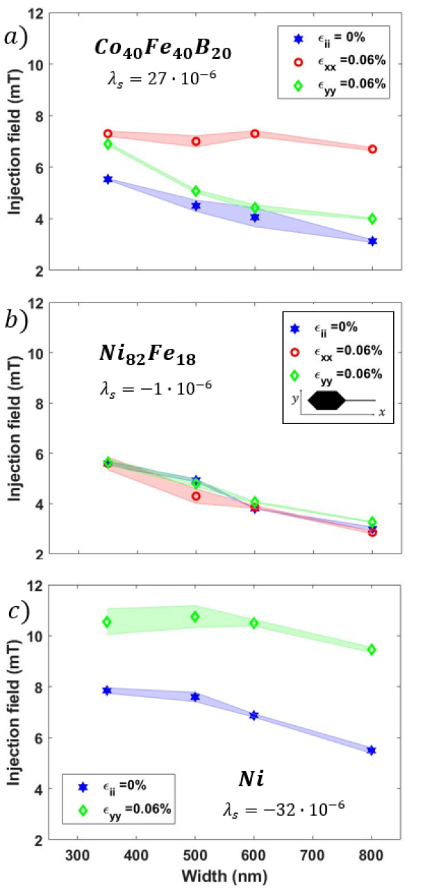
In figure 4, the injection field is experimentally reported for three different materials. As expected, materials with strong magnetoelastic coupling (i.e. large ) will show the largest strain effects as can be seen in figure 4 a) and c). This is why, for , with low magnetoelastic coupling, the three curves overlap within the error bars in figure 4 b). This also confirms that the observed changes in the injection field are caused by strain.
A first observation is that in magnetostrictive materials strain is always increasing the injection field, thus imposing a lower limit for the sensor operation field. When an easy axis along is created, the pad coercivity grows, thus also increasing the injection field. This is the case of for and for . When instead the easy axis is oriented along the direction ( for and for ), the DW created at the mouth of the pad finds this position more energetically favorable than the wire. Therefore, a larger injection field is required. Due to small magnetic contrast in , some experimental points in 4 c) are missing.
A second observation concerns the wire width dependence of the injection field. Regardless of the material, when strain is not applied (), we find that the injection field decreases with the increasing width of the wire. As reported elsewhereIm et al. (2009); Bogart et al. (2009), the injection field in soft magnetic wires is mainly determined by the shape of the cross section (width and thickness) and the monotonic behavior of is the consequence of different sizes of DWs governed by different wire widths. Therefore, we expect that in the absence of strain the de-pinning field from the extremity of the pad is mainly due to shape anisotropy Backes et al. (2007). However, when magnetoelastic anisotropy energy is introduced in the system, we observe deviation from this dependence. When favors a spin orientation along the direction, the injection field is determined by the coercivity of the pad and the dependence of the injection field on the wire width is negligible for thin wires (figure 4 a), red circles and 4 c), green diamonds). This is because in the pad is large enough to inject and propagate the DW through the nanowire. In all the other measured cases, instead, the DW stays pinned at the edge of the pad, and a net dependence of on the wire width is observable. Interestingly, when the strain-induced easy axis of magnetization is perpendicular to the wire, the dependence of on the wire width is stronger (figure 4 a), green diamonds).
An explanation for this can be found in the different competing contributions to the system energy. To describe the impact of strain on the magnetization orientation and injection field, we use the free energy of the system that is a measure for the angular dependence of the magnetic hardness. In a system with no net crystalline anisotropy, the free energy is given byWeiler et al. (2009); Brandlmaier et al. (2008)
| (2) |
describes the influence of the external magnetic field, and the demagnetization term depends on the shape of the device. The last term describes the influence of the lattice strain to the magnetic anisotropy according to equation 1, where is the angle between the magnetization and the easy axis. Minima in the expression of correspond to magnetic easy directions.
Let us now compare the case of (no strain) and with the easy axis along y. This strain-induced uniaxial anisotropy tends to favor a spin configuration with wider DW in the nucleation pad, where a large part of magnetization is pointing along y. This is observed both in the MOKE images and in the simulated spin structure. What determines the injection fieldBogart et al. (2009), is the energy difference between a DW sitting at the extremity of the pad and inside the wire . Since in the wire a narrow DW is preferredMcMichael and Donahue (1997), the energy barrier will be larger if . Therefore, a larger external applied field is required to inject the DW wall, as we experimentally observe.
To get a better understanding of the effect of strain on the injection field we performed micromagnetic simulations using the GPU-based framework Vansteenkiste et al. (2014). The material parameter values measured for our sample were considered, namely and for saturation magnetostriction and magnetization, respectively, whereas for the exchange and elastic constants typical values for reported in the literature were used Peng et al. (2016): , , and .
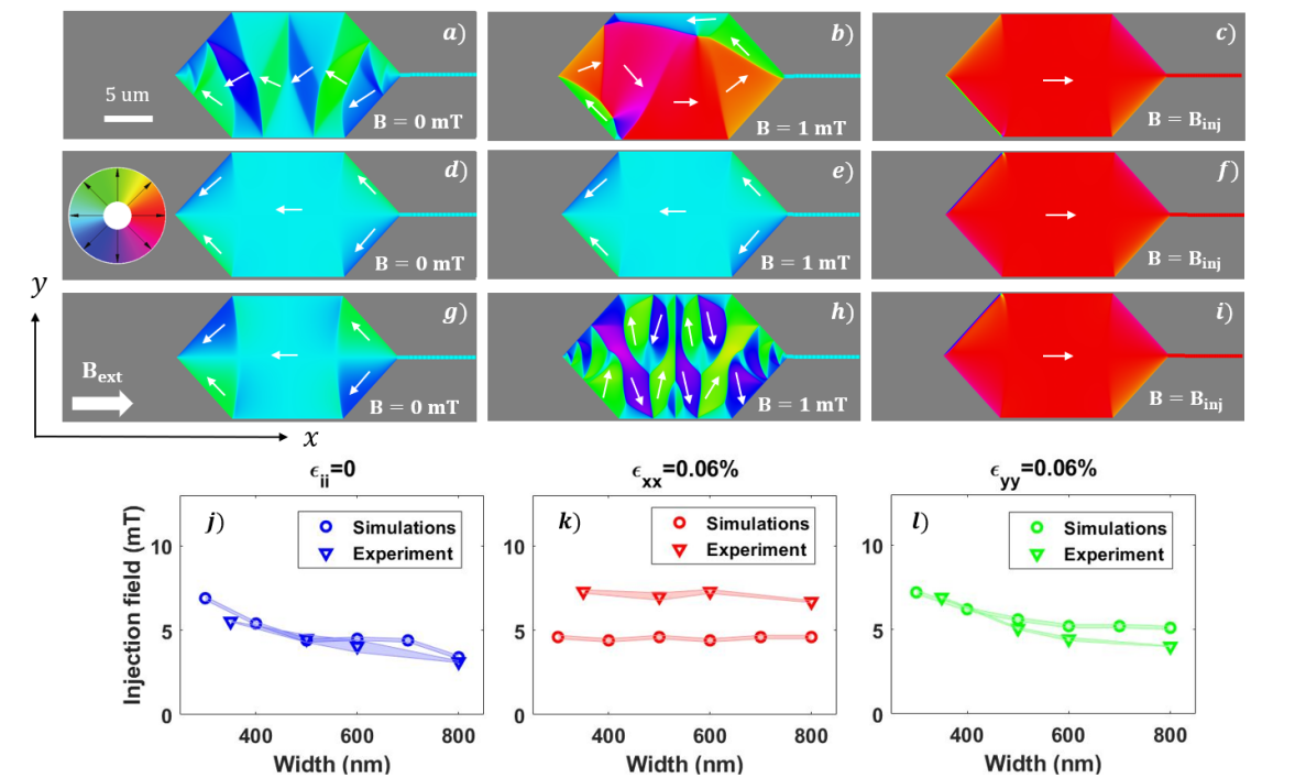
In the simulations the dimensions of the pad are the same than in the physical system (figure 1 c)), whereas the nanowire is shortened to . The computational region is divided into cells. The mechanical stress is modeled by adding a magnetoelastic field contribution to the effective field Yanes et al. (2019); Hubert and Schäfer (2008). The system is initialized with uniform magnetization pointing in the direction and the equilibrium state is calculated for a series of increasing applied fields in steps of . The results of the simulations are shown in figure 5. Some snapshots of the magnetization are presented to be compared with the Kerr microscope images in figure 3. As noticeable, the main features observed at are reproduced by the simulations, namely the double vortex pattern in the absence of strain (figures 3 b) and 5 b)), the quasi-uniform configuration for (figures 3 e) and 5 e)) and the multidomain state favoring the magnetization pointing along y for (figures 3 h) and 5 h)). The computed injection fields as a function of the wire width are plotted in the lower part of figure 5 together with the experimental ones, showing good quantitative agreement except for the case where the tensile strain is applied along x, where the computed values are significantly below the experimental ones. Both the decrease in the injection field when increasing the wire width for the cases of no strain (figure 5 j)) and (figure 5 l)) and the negligible dependence for are well captured by the simulations, supporting our interpretation of the experimental results.
To summarize, an overview of the effects of the strain on the injection field can be observed in figure 4 a). We report that for a positive magnetostrictive material such as , uniaxial strain increases the injection field. In the case when the easy axis of magnetization is aligned along the wire, the injection field coincides with of the pad and the wire width dependence is low (figure 4 a), red circles).
III.2 Effects of growth induced anisotropy
Up to now we have considered isotropic and magnetically soft ferromagnetic materials. In this case, a strain induced uniaxial anisotropy with constant of was the only anisotropy energy contribution in the full film material. To further investigate the mechanism and the limits for DW nucleation and injection, we structured our devices using thermally annealed . This material preparation induces a preferential orientation (easy axis, EA) for the magnetization, according to the direction of the applied magnetic field during annealing. The uniaxial anisotropy has been measured experimentally from the full film hysteresis loops. To take this contribution into account, an additional term to the free energy is added, and equation 2 becomes
| (3) |
where is the free energy term of the crystalline magnetic anisotropy, which may compete with strain-induced anisotropy and alter the magnetization orientation effects.
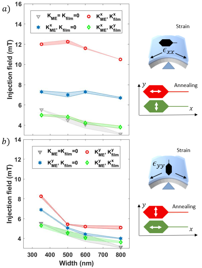
In light of this, the experiment described in the previous section has been repeated for annealed samples. Sizable effects are found when and the magnetoelastic anisotropy are superimposed. In figure 6, the results for this experiment are shown, and the annealed films are compared with the as-deposited samples. One can observe how, when the directions of and are parallel, the effects of strain are enhanced (larger injection field for red points in figure 6). On the other hand, strain effects are attenuated or compensated if and have perpendicular easy axis direction (green points in figure 6). When two different uniaxial anisotropy contributions point in the same direction, the resulting anisotropy of the film is still uniaxial, but now has an equivalent anisotropy constant . This is experimentally confirmed by an increase in the anisotropy field , measured along the hard axis of magnetization. Again, we can distinguish two situations. When and are oriented along , the resulting EA is along the wire (figure 6 a), red circles). This increases the coercive field of the pad and consequently the injection field also grows. When and are oriented with EA along , the resulting anisotropy favors energetically the DW to be positioned at the extremity of the pad. Consequently and are larger (figure 6 b), red circles).
The nontrivial case is the situation when the two contributions of anisotropy, and , are perpendicular to each other. Experimentally, the values of the injection field are reduced and are close to the non-strained sample (gray triangles in figure 6). This result is important since it shows that strain effects on the device can be attenuated by material preparation. This outcome might seem unexpected, due to the difference in strength of the two contributions and . However, one should keep in mind that the idea of an "effective" uniaxial magnetic anisotropy is not applicable, unless the anisotropy are oriented along identical directions.
To understand these results, a characterization of the full film material has been done in the presence of strain and annealing-induced anisotropy with MOKE hysteresis loops. The most general case considers a magnetic energy described by two perpendicular uniaxial magnetic anisotropies axes. We have measured the angular dependence of the normalized remanent magnetization as function of the angle between the external magnetic field and the easy axis of magnetization. In figure 7 the cases , and , are compared. In both cases, the strain is defining the dominant easy axis, since . However, in figure 7 we observe differences in the angular plots of in the vicinity of the hard axis (90∘). The precise determination of the magnetic easy axis is carried out by fitting the normalized magnetic hysteresis curves as a function of . The projection of the in-plane magnetization vector to the plane of incidence of light during our MOKE measurements is a cosine-like function (as is evident from the inset in figure 7), therefore, the following fitting function is chosen Mollick et al. (2018):
| (4) |
where is the maximum normalized magnetic remanence, and is the offset in magnetic remanence . The strength of the uniaxial magnetic anisotropy is the amplitude of the fitting parameter, and the offset originates from the isotropic contribution of the film.
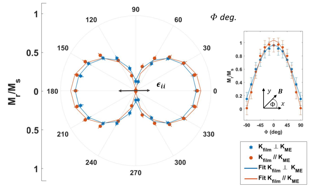
The fitting confirms that the easy axis is along (strain direction). However, the strength of the dominant magnetic easy axis is strongly reduced when . More quantitatively, if we compare the two cases and , the offset increases from to while the maximum remanence decreases from to , respectively. This means the annealing induced anisotropy can contribute to the effective magnetic anisotropy of the system. The pure uniaxial anisotropy is modified by the presence of an isotropic part.
The observed results and consideration on the full film material properties can explain the experimentally determined injection field. In figure 6, we showed how the effects of strain can be compensated by annealing with a magnetic field perpendicular to the strain direction. In a material with larger the coherent rotation of the magnetization requires less energy: the anisotropy field decreases and the coercive field is reduced at the same time. Therefore, the film becomes magnetically softer, and the magnetic properties of the blue points in figure 7 are closer to the ones of the unstrained as-deposited state, shown in figure 2 a). This supports the findings displayed in figure 6, where the green () and gray (no anisotropy) data points overlap.
The material softness directly influences not only the creation and nucleation of the DW in the nucleation pad, but also the injection field, due to the fact that the energy difference between the DW at the mouth of the pad and in the nanowire is affected by the film properties. We can indeed say that the DW energy in the thin long wire is unchanged by the presence of an annealing-induced anisotropy, because here the strong shape anisotropyKumar et al. (2006) is in the order of . On the other hand, in the nucleation pad, if the strength of the uniaxial magnetic anisotropy is reduced, the magnetization is free to rotate in the field direction similarly to the unstrained as-deposited state.
IV Conclusions
In conclusion, we have investigated the effects of mechanical strain on the injection of a DW into a nanowire using MOKE microscopy and micromagnetic simulations. We have measured in-plane magnetized , and films structured by optical lithography. We find that the effects of the strain are proportional to the magnetoelastic coupling of the material, quantified by the saturation magnetostriction . We report that uniaxial strain, regardless of the direction, induces a uniaxial magnetic anisotropy in the material and increases the injection field. The changes are up to in materials with , while are negligible in low magnetostrictive . The experimental results show how the mechanism of DW injection depends primarily on the creation of the DW in the pad. Further measurements involved different material preparation introducing a thermal annealing step with a magnetic field for . With this, another uniaxial magnetic anisotropy is introduced, and contributes together with strain effects to the . We find that the strain induced uniaxial anisotropy, , can be enhanced or weakened using annealing induced uniaxial anisotropy, , respectively, parallel or perpendicular to the strain contribution. If the easy axis of magnetization is along the wire direction, the coercive field of the nucleation pad increases significantly. In the same way, low anisotropy will facilitate the magnetization to switch, and creates a DW at low fields () at the extremity of the pad. The DW stays pinned at the wire entrance until the energy difference is comparable with the Zeeman energy (higher external fields). This energy barrier is the combination of different anisotropies, and can be tailored by device design and material preparation. The validity of these results is verified by micromagnetic simulations, that can help to identify the lower limit for reliable DW injection. The optimization and development of magnetic sensors and devices based on domain walls needs to consider, therefore, the effects of strain and material preparation. Our results of the DW injection mechanism show that a magnetostrictive free behavior of the DW based device, can even be reached in systems with finite magnetostriction. A careful material preparation, can reduce the effective anisotropy caused by strain in the magnetic layer thus keeping the DW injection field low in these devices. This provides, therefore, a way to improve robustness of these type of magnetic sensors against strain disturbances.
Acknowledgements.
The authors would like to acknowledge Dr. R. Lehndorff for the fruitful discussions. This project has received funding from the European Union’s Horizon 2020 research and innovation program under the Marie Skłodowska-Curie grant agreement No 860060 “Magnetism and the effect of Electric Field” (MagnEFi) and the Austrian Research Promotion Agency (FFG). The authors also acknowledge support by the chip production facilities of Sensitec GmbH (Mainz, DE), where part of this work was carried out and the Max-Planck Graduate Centre with Johannes Gutenberg University.Data Sharing Policy
The data that support the findings of this study are available from the corresponding author upon reasonable request. This article has been submitted to Journal of Applied Physics. After it is published, it will be found on the AIP Publishing website .
References
- Kläui (2008) M. Kläui, “Head-to-head domain walls in magnetic nanostructures,” Journal of Physics: Condensed matter 20, 313001 (2008).
- Spain (1966) R. Spain, “Domain tip propagation logic,” IEEE Transactions on Magnetics 2, 347–351 (1966).
- Parkin, Hayashi, and Thomas (2008) S. S. Parkin, M. Hayashi, and L. Thomas, “Magnetic domain-wall racetrack memory,” Science 320, 190–194 (2008).
- Jogschies et al. (2015) L. Jogschies, D. Klaas, R. Kruppe, J. Rittinger, P. Taptimthong, A. Wienecke, L. Rissing, and M. C. Wurz, “Recent developments of magnetoresistive sensors for industrial applications,” Sensors 15, 28665–28689 (2015).
- Diegel, Mattheis, and Halder (2007) M. Diegel, R. Mattheis, and E. Halder, “Multiturn counter using movement and storage of 180° magnetic domain walls,” Sensor Letters 5, 118–122 (2007).
- Mattheis et al. (2012) R. Mattheis, S. Glathe, M. Diegel, and U. Hübner, “Concepts and steps for the realization of a new domain wall based giant magnetoresistance nanowire device: From the available 24 multiturn counter to a 212 turn counter,” Journal of Applied Physics 111, 113920 (2012).
- Borie et al. (2017a) B. Borie, J. Wahrhusen, H. Grimm, and M. Kläui, “Geometrically enhanced closed-loop multi-turn sensor devices that enable reliable magnetic domain wall motion,” Applied Physics Letters 111, 242402 (2017a).
- Borie et al. (2017b) B. Borie, A. Kehlberger, J. Wahrhusen, H. Grimm, and M. Kläui, “Geometrical dependence of domain-wall propagation and nucleation fields in magnetic-domain-wall sensors,” Physical Review Applied 8, 024017 (2017b).
- Martinez et al. (2007) E. Martinez, L. Lopez-Diaz, O. Alejos, L. Torres, and C. Tristan, “Thermal effects on domain wall depinning from a single notch,” Physical Review Letters 98, 267202 (2007).
- Martinez et al. (2009) E. Martinez, L. Lopez-Diaz, O. Alejos, L. Torres, and M. Carpentieri, “Domain-wall dynamics driven by short pulses along thin ferromagnetic strips: Micromagnetic simulations and analytical description,” Physical Review B 79, 094430 (2009).
- Garcia-Sanchez et al. (2011) F. Garcia-Sanchez, A. Kakay, R. Hertel, and P. Asselin, “Depinning of transverse domain walls from notches in magnetostatically coupled nanostrips,” Applied physics express 4, 033001 (2011).
- Hoang et al. (2020) D.-Q. Hoang, X.-H. Cao, H.-T. Nguyen, and V.-A. Dao, “Creation and propagation of a single magnetic domain wall in 2D nanotraps with a square injection pad,” Nanotechnology 32, 095703 (2020).
- Van Driel et al. (2003) W. Van Driel, J. Janssen, G. Zhang, D. Yang, and L. Ernst, “Packaging induced die stresses-effect of chip anisotropy and time-dependent behavior of a molding compound,” Journal of Electronic Packaging 125, 520–526 (2003).
- Lee (1955) E. W. Lee, “Magnetostriction and magnetomechanical effects,” Reports on Progress in Physics 18, 184 (1955).
- Finizio et al. (2014) S. Finizio, M. Foerster, M. Buzzi, B. Krüger, M. Jourdan, C. A. Vaz, J. Hockel, T. Miyawaki, A. Tkach, S. Valencia, et al., “Magnetic anisotropy engineering in thin film Ni nanostructures by magnetoelastic coupling,” Physical Review Applied 1, 021001 (2014).
- Lei et al. (2013) N. Lei, T. Devolder, G. Agnus, P. Aubert, L. Daniel, J.-V. Kim, W. Zhao, T. Trypiniotis, R. P. Cowburn, C. Chappert, et al., “Strain-controlled magnetic domain wall propagation in hybrid piezoelectric/ferromagnetic structures,” Nature Communications 4, 1–7 (2013).
- Cowburn et al. (2002) R. Cowburn, D. Allwood, G. Xiong, and M. Cooke, “Domain wall injection and propagation in planar permalloy nanowires,” Journal of Applied Physics 91, 6949–6951 (2002).
- Shigeto, Shinjo, and Ono (1999) K. Shigeto, T. Shinjo, and T. Ono, “Injection of a magnetic domain wall into a submicron magnetic wire,” Applied Physics Letters 75, 2815–2817 (1999).
- Zhou et al. (2020) H. Zhou, S. Shi, D. Nian, S. Cui, J. Luo, Y. Qiu, H. Yang, M. Zhu, and G. Yu, “Voltage control of magnetic domain wall injection into strain-mediated multiferroic heterostructures,” Nanoscale 12, 14479–14486 (2020).
- Choe and Megdal (1999) G. Choe and B. Megdal, “High precision magnetostriction measurement employing the BH looper bending method,” IEEE Transactions on Magnetics 35, 3959–3961 (1999).
- Hill et al. (2013) C. Hill, W. Hendren, R. Bowman, P. McGeehin, M. Gubbins, and V. Venugopal, “Whole wafer magnetostriction metrology for magnetic films and multilayers,” Measurement Science and Technology 24, 045601 (2013).
- Raghunathan, Snyder, and Jiles (2009) A. Raghunathan, J. E. Snyder, and D. Jiles, “Comparison of alternative techniques for characterizing magnetostriction and inverse magnetostriction in magnetic thin films,” IEEE Transactions on Magnetics 45, 3269–3273 (2009).
- Cullity and Graham (2011) B. D. Cullity and C. D. Graham, Introduction to magnetic materials (John Wiley & Sons, 2011).
- Zhang et al. (2011) Y. Zhang, X. Fan, W. Wang, X. Kou, R. Cao, X. Chen, C. Ni, L. Pan, and J. Q. Xiao, “Study and tailoring spin dynamic properties of CoFeB during rapid thermal annealing,” Applied Physics Letters 98, 042506 (2011).
- Thomas et al. (2003) O. Thomas, Q. Shen, P. Schieffer, N. Tournerie, and B. Lépine, “Interplay between anisotropic strain relaxation and uniaxial interface magnetic anisotropy in epitaxial Fe films on (001) GaAs,” Physical Review Letters 90, 017205 (2003).
- McGrouther et al. (2007) D. McGrouther, S. McVitie, J. Chapman, and A. Gentils, “Controlled domain wall injection into ferromagnetic nanowires from an optimized pad geometry,” Applied Physics Letters 91, 022506 (2007).
- Wang (2019) J. Wang, “Mechanical control of magnetic order: from phase transition to skyrmions,” Annual Review of Materials Research 49, 361–388 (2019).
- Bur et al. (2011) A. Bur, T. Wu, J. Hockel, C.-J. Hsu, H. K. Kim, T.-K. Chung, K. Wong, K. L. Wang, and G. P. Carman, “Strain-induced magnetization change in patterned ferromagnetic nickel nanostructures,” Journal of Applied Physics 109, 123903 (2011).
- Im et al. (2009) M.-Y. Im, L. Bocklage, P. Fischer, and G. Meier, “Direct observation of stochastic domain-wall depinning in magnetic nanowires,” Physical Review Letters 102, 147204 (2009).
- Bogart et al. (2009) L. Bogart, D. Atkinson, K. O’Shea, D. McGrouther, and S. McVitie, “Dependence of domain wall pinning potential landscapes on domain wall chirality and pinning site geometry in planar nanowires,” Physical Review B 79, 054414 (2009).
- Backes et al. (2007) D. Backes, C. Schieback, M. Kläui, F. Junginger, H. Ehrke, P. Nielaba, U. Rüdiger, L. J. Heyderman, C.-S. Chen, T. Kasama, et al., “Transverse domain walls in nanoconstrictions,” Applied Physics Letters 91, 112502 (2007).
- Weiler et al. (2009) M. Weiler, A. Brandlmaier, S. Geprägs, M. Althammer, M. Opel, C. Bihler, H. Huebl, M. S. Brandt, R. Gross, and S. T. Gönnenwein, “Voltage controlled inversion of magnetic anisotropy in a ferromagnetic thin film at room temperature,” New Journal of Physics 11, 013021 (2009).
- Brandlmaier et al. (2008) A. Brandlmaier, S. Geprägs, M. Weiler, A. Boger, M. Opel, H. Huebl, C. Bihler, M. S. Brandt, B. Botters, D. Grundler, et al., “In situ manipulation of magnetic anisotropy in magnetite thin films,” Physical Review B 77, 104445 (2008).
- McMichael and Donahue (1997) R. D. McMichael and M. J. Donahue, “Head to head domain wall structures in thin magnetic strips,” IEEE Transactions on Magnetics 33, 4167–4169 (1997).
- Vansteenkiste et al. (2014) A. Vansteenkiste, J. Leliaert, M. Dvornik, M. Helsen, F. Garcia-Sanchez, and B. Van Waeyenberge, “The design and verification of MuMax3,” AIP Advances 4, 107133 (2014).
- Peng et al. (2016) R.-C. Peng, J.-M. Hu, K. Momeni, J.-J. Wang, L.-Q. Chen, and C.-W. Nan, “Fast 180° magnetization switching in a strain-mediated multiferroic heterostructure driven by a voltage,” Scientific Reports 6, 1–9 (2016).
- Yanes et al. (2019) R. Yanes, F. Garcia-Sanchez, R. Luis, E. Martinez, V. Raposo, L. Torres, and L. Lopez-Diaz, “Skyrmion motion induced by voltage-controlled in-plane strain gradients,” Applied Physics Letters 115, 132401 (2019).
- Hubert and Schäfer (2008) A. Hubert and R. Schäfer, Magnetic domains: the analysis of magnetic microstructures (Springer Science & Business Media, 2008).
- Mollick et al. (2018) S. A. Mollick, R. Singh, M. Kumar, S. Bhattacharyya, and T. Som, “Strong uniaxial magnetic anisotropy in Co films on highly ordered grating-like nanopatterned Ge surfaces,” Nanotechnology 29, 125302 (2018).
- Kumar et al. (2006) A. Kumar, S. Fähler, H. Schloerb, K. Leistner, and L. Schultz, “Competition between shape anisotropy and magnetoelastic anisotropy in Ni nanowires electrodeposited within alumina templates,” Physical Review B 73, 064421 (2006).
- Gabor et al. (2011) M. Gabor, T. Petrisor Jr, C. Tiusan, M. Hehn, and T. Petrisor, “Magnetic and structural anisotropies of heusler alloy epitaxial thin films,” Physical Review B 84, 134413 (2011).