Indirect light absorption model for highly strained silicon infrared sensors
Abstract
The optical properties of silicon can be greatly tuned by applying strain, opening new perspectives particularly in applications where infrared is key. In this work, we use a recent model for the indirect light absorption of silicon and include the effects of tensile and compressive uniaxial strains. The model is based on material properties such as the band gap, the conduction and valence bands density-of-states effective masses, and the phonon frequencies, that are obtained from first principles including strain up to % along the [110] and [111] directions. We show that the limit of absorption can increase from 1.14 m (1.09 eV) to 1.35 m (0.92 eV) under 2% strain, and that the absorption increases by a factor of 55 for the zero-strain cutoff wavelength of 1.14 m when a 2% compressive strain is applied in the [110] direction. We demonstrate that this effect is mainly due to the impact of strain on the electronic band gaps of silicon, directly followed by the valence band density-of-states effective mass.
I Introduction
Silicon is a well-known material in the electronic industry. It has been extensively used over the past decades to develop ever more efficient electronic devices. Compared to other materials used in infrared applications, e.g., germanium, indium or gallium,[1] silicon devices present the advantages of low toxicity and environmental impact with straightforward integration for CMOS circuits. Most improvements were realized by reducing the device dimensions.[2] However, reducing dimensions has physical limits, and other technical innovations have been needed. [3] Strained silicon has been suggested and indeed quickly showed promising properties such as improved electron or hole mobilities.[4, 5] This technique is now widely used in industry especially to enhance Si-based CMOS performances with a mobility increase up to 90% with stressors or epitaxial growth.[6] Today, strain engineering is used routinely to manufacture semiconductor devices, in order to boost performances at low additional cost.[7, 8, 9] Even though the effects of small strain on the electronic properties of silicon have already been studied, both theoretically and experimentally,[10, 11, 12] highly strained silicon remains largely unexplored. Only recently, it was shown how to reach high strain in different structures based on nanoribbons[13, 14, 15], nanowires[16] or nanomembranes.[17, 18] The interest for highly strained silicon is therefore enhanced since such strain levels can significantly change its optical properties and make silicon a suitable material for infrared applications.[19, 20, 21, 22, 23, 24]
The indirect band gap of silicon enables light absorption through interband transitions up to the near-infrared region, for photon energies roughly larger than the fundamental band gap of 1.12 eV at 300 K (wavelengths lower than 1.1 m).[25] Such indirect transitions require additional momenta provided by the lattice vibrations, the so-called phonons.[26] This phonon-assisted process dominates the absorption spectrum of silicon in the energy region between the fundamental and the direct (3.2 eV) band gaps. For energies larger than the direct band gap, the absorption quickly increases and is mainly dictated by direct interband transitions. Despite the importance of the subject, only a few theoretical computations of the indirect absorption spectrum of silicon exist,[26, 27, 28, 29] mostly because of the complexity of the interactions between electrons and phonons.[30] Only recently, first-principles computations of the phonon-assisted absorption were able to quantitatively describe the absorption spectrum of silicon.[26, 27] However, while these first-principles computations give accurate results, the computational cost is very large.
In this work, we extend the theoretical model of Tsai[28] developed for relaxed silicon to the highly strained crystal case. The model requires only a few parameters such as the direct and indirect band gaps, the conduction and valence bands density-of-states effective masses (i.e., the effective masses leading to the same density of states as if the bands were parabolic), the phonon frequencies, and the deformation potentials for the different electronic transitions. Using first-principles computations, we show that the main impact of strain is on the band gaps and the effective masses, while the phonon energies remain almost unchanged. The advantage of this model compared with fully first-principles computations is the time required to obtain the full spectrum, particularly when many strain levels have to be considered. Using our model, we demonstrate that the cutoff wavelength of silicon, defined here as the wavelength above which the absorption becomes lower than cm-1, can increase from 1.14 to 1.35 m (decrease from 1.09 to 0.92 eV) under a 2% tensile or compressive strain. Additionally, we show that the absorption coefficient increases by a factor of 15 to 55 at the zero-strain cutoff wavelength, therefore largely increasing the efficiency of silicon-based devices in the infrared.
II Indirect light absorption model
Light absorption can be due to direct and indirect processes. In this work, we focus on the indirect light absorption, which is the dominating process for photons of energies below 3.2 eV (above 387 nm) in relaxed silicon. In this case, the absorption coefficient is usually expected to vary as the square of the incoming photon energy , with the photon wavelength. More precisely, assuming single-phonon processes, the absorption coefficient can be expressed as[31]
| (1) |
where is a material-dependent coefficient, is the fundamental band gap, is the phonon energy, is the Boltzmann constant, is the temperature and is the Heaviside unit-step function. The two terms in Eq. (1) correspond to phonon absorption and emission processes, respectively. This equation can correctly describe the general trend of the absorption spectrum.[32] It can also be used to extract band gap values (the absorption coefficient being very low for photon energies below the fundamental band gap).[31] In this relation, is treated as a fitting parameter of the semi-empirical model. Therefore, this a priori unknown proportionality coefficient prevents a fully theoretical prediction of materials performances, particularly in a case such as highly strained silicon for which there are no experimental data available.
Recently, Tsai derived a theoretical model for computing the indirect absorption coefficient based on second-order time-dependent perturbation theory.[28] The model extends Eq. (1) by considering all the possible types of intervalley scattering processes for the indirect transitions. Some of these transitions are represented in Fig. 1 with the band structure of relaxed silicon. Such indirect light absorption happens by either the absorption of a photon (represented by blue arrows) followed by the absorption or emission of a phonon (represented by red wavy arrows), or vice versa.
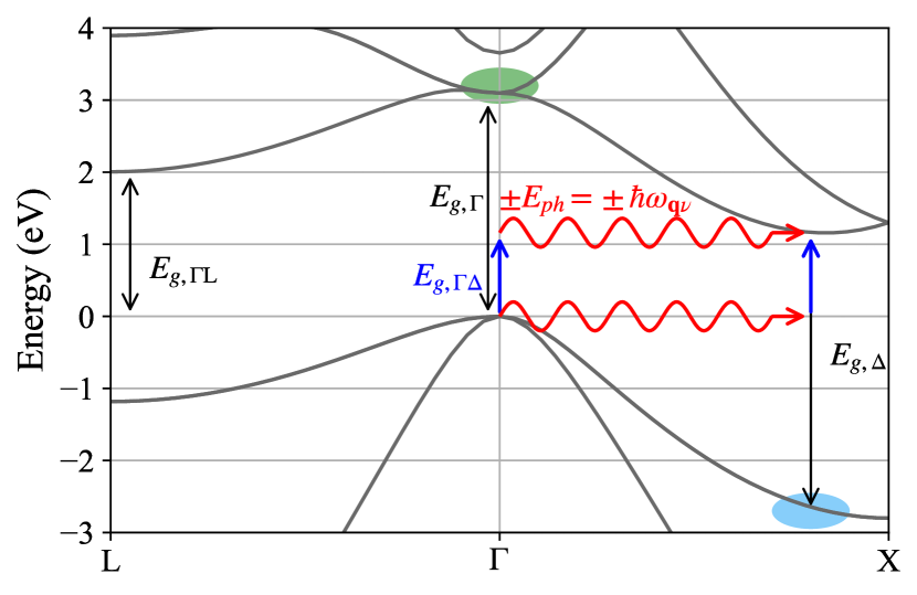
For each valley of the conduction band where the electrons might be scattered, two intermediate states are considered. The first one (in green in Fig. 1) is located at in the conduction band, and the second one (in blue in Fig. 1) is located in the valence band, at the high-symmetry point characterizing the conduction band valley (denoted by in the following), being the electron wavevector. For a given transition connecting two valleys through a phonon of wavevector and mode , the absorption coefficient derived by Tsai is given by[28]
| (2) |
where is the number of degenerated conduction valleys, is the indirect band gap (fundamental or not, depending on the considered valley), and are the direct band gap energies providing intermediate states (for instance, and in Fig. 1), is a damping factor, and
| (3) |
is the Bose-Einstein distribution for the number of phonons of frequency . The material-dependent proportionality constant is defined as
| (4) |
where is the electron charge, is the free electron mass, is the speed of light in vacuum, is the material density, is the refractive index, is an energy parameter for the electron-photon interactions, is the phonon deformation potential, and and denote the density-of-states effective masses of the conduction and valence bands, respectively. To the contrary of the semi-empirical model, Eq. (2) is based on a fully detailed physical understanding of the absorption mechanisms that is essential to correctly predict the behavior of the material.
As it is observed in Fig. 1, different indirect transitions have to be considered in silicon, corresponding to different valleys of the conduction band. Each of them gives a different contribution to the total absorption coefficient,
| (5) |
III Methods
III.1 Strain
We consider two crystallographic directions for the uniaxial strain, namely [110] and [111]. These modify the unit cell of silicon according to the related strain tensors,
| (6) |
| (7) |
where is the uniaxial strain applied on the material in the [110] or [111] direction while is the induced perpendicular strain. For elastic deformations, is proportional to :
| (8) |
with
| (9) |
and
| (10) |
where GPa, GPa, and GPa are the elastic constants of silicon.[33]
III.2 Computational methods
For relaxed and strained silicon, different parameters are computed from first principles using density functional theory (DFT), as implemented in ABINIT.[34, 35] We use norm-conserving pseudopotentials from the PseudoDojo,[36] in the generalized-gradient approximation (GGA) from Perdew-Burke-Ernzerhof (PBE) with a plane-wave cutoff of 20 Ha. For each strain level, we first perform a structural relaxation for the two atoms of the strained (fixed) unit cell. The electronic band structure is then determined using an 888 Monkhorst-Pack -point grid.[37] As expected from DFT, the band gaps are severely underestimated. This is corrected by applying scissor shifts to the conduction band levels in order to fit the experimental measurements for relaxed silicon. The same scissor shifts are kept for the strained cases.
The phonon frequencies are obtained within density-functional perturbation theory (DFPT) using ABINIT.[38, 39] The deformation potentials are considered constant, as justified later in this work. Finally, each conduction band valley is considered separately since their degeneracy is lifted by the strain. The absorption coefficient is then obtained as the sum of all these separate contributions.
The density-of-states effective mass of a given band (conduction or valence) is defined as the one giving the same density of states as if the band was parabolic. In the case of the valence band, it is obtained through[40, 41]
| (11) |
where is the energy of the valence band maximum and is the density of states obtained on dense meshes for each strained configuration. A similar expression holds for the conduction band. In the case of silicon, the conduction band is almost perfectly parabolic so that is very close to the geometric mean of the transverse and longitudinal components of the electron effective mass tensor, and , respectively,[42]
| (12) |
where denotes a single valley. These longitudinal and transverse electron effective masses can be determined as second-order derivatives of the electronic energies, obtained from non-self-consistent computations of the band structure on dense meshes. In contrast, the top of the valence band does not consist of a single state and is highly anisotropic and non-parabolic so that a formula such as Eq. (12) does not hold.
IV Indirect absorption in relaxed silicon
In relaxed silicon, the only contribution for the absorption of infrared light ( nm) comes from the transitions to the valleys, where the conduction band minimum of silicon lies. The indirect band gap is 1.12 eV and the valley is 6-fold degenerated. The transitions to other higher-energy valleys, such as L (see Fig. 1) or even K and U, are also responsible for visible light absorption for eV ( nm). In this work, we focus on the region of the spectrum between 0.89 and 1.91 eV (0.65 and 1.4 m). Therefore, only the contributions from the six degenerated valleys need to be included in the case of relaxed silicon, and only three gaps have to be considered in Eq. (2): the direct band gaps at and ( and , respectively) and the fundamental gap , see Fig. 1. The experimental values are used in relaxed silicon, as explained in our methodology.
Different phonon modes have to be considered for the intervalley transitions. In silicon, 6 modes are present and should be taken into account. Following Ridley,[43] Tsai included only the transverse optical (TO) and acoustic (TA) modes.[28] However, it has recently been shown by Vandenberghe et al. that the deformation potential for the longitudinal optical (LO) mode is far from being negligible,[44] while the longitudinal acoustic (LA) mode can be safely ignored.[44] Therefore, we also include the contribution of the LO mode and use these deformation potentials, that are given in Table 1. The values used by Tsai are given in brackets for comparison.
| Parameters | Value |
|---|---|
| 3.42 | |
| 2.328 g/cm3 | |
| 0.36 (0.328) | |
| 0.81 (0.55) | |
| T | 300 K |
| 12 (25) eV | |
| 1.35 eV | |
| 3.2 eV | |
| 1.12 (1.1557) eV | |
| 4 eV | |
| () eV/cm | |
| () eV/cm | |
| () eV/cm |
We obtain the conduction and valence bands density-of-states effective masses using the methodology described in the previous section and obtain different values as the ones used by Tsai, see Table 1. Particularly, the valence band effective mass is % larger but in better agreement with experimental evidence.[45] The conduction band effective mass is also in good agreement with previous results.[46, 47, 45] The parameter related to the electron-photon interactions is also adapted to better fit the experimental absorption coefficient. All the other parameters required by the indirect-light absorption model are given in Table 1.
Figure 2 compares the absorption coefficient obtained by Tsai (including only the TO and TA modes, and using the parameters in brackets in Table 1) with our result obtained by taking into account the LO mode and the deformation potentials from Vandenberghe et al.,[44] evaluated at the point connecting the valence band maximum to the conduction band minimum (), and our computed effective masses. The contributions of the different modes are further analyzed in the inset of Fig. 2.
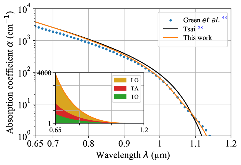
In order to evaluate this model, the data from Green et al.[48] for the absorption coefficient of silicon is also represented in Fig. 2. Due to its availability, this data set is usually taken as a reference for silicon absorption to compare and check the validity of different absorption models. It can be seen from Fig. 2 that the agreement between Tsai results, ours, and the experimental data is very good on a large portion of the spectrum. However, close to the cutoff wavelength of 1.14 m, our model allows for a better description of the shape of the absorption spectrum, in contrast with the case where the LO mode is not taken into account. Indeed, this mode is dominating the absorption coefficient spectrum and should not be neglected, particularly in the region of interest for near-infrared applications.
In the following, we extend this model to take into account the impact of strain on the absorption of silicon using DFT and DFPT to compute the evolution of important parameters such as the effective masses, the band gaps and the phonons energies. This allows us to efficiently compute and predict the optical properties of highly-strained silicon.
V Highly strained silicon
V.1 Electronic band structure
In the energy region of interest, i.e., 0.89–1.91 eV, only the indirect absorption through the valleys have to be considered in the case of relaxed silicon. For strained-silicon, we also need to monitor the indirect band gaps between the valence band maximum at and other valleys of the conduction band, such as L, K, or U (, and , respectively). Indeed, even if these indirect gaps are larger than 1.91 eV at zero strain, they could decrease and lead to important contributions to the absorption spectrum of highly strained silicon. Table 2 gives the band gaps obtained with DFT, together with the experimental values and the applied scissor shifts.
| DFT | Expts.[49] | Scissor | |
|---|---|---|---|
| 0.61 | 1.12 | 0.51 | |
| 2.55 | 3.2 | 0.65 | |
| 3.28 | 4 | 0.72 | |
| 1.46 | 2.5 | 1.04 | |
| 1.24 | - | 1.04 | |
| 1.24 | - | 1.04 |
The scissor shifts are different for each transition, because the underestimation of the gap is not uniform. In general, the shift of the conduction band energies increases with the electron energy.[50] In this work, we fix the scissor shifts depending on the experimental values of the gaps in relaxed silicon, and keep the same values for the strained cases. Since the L, U, and K valleys have similar energies, we apply the same scissor shift to the corresponding gaps.
When a uniaxial strain along the [110] direction is applied, some crystal symmetries are broken which lifts the degeneracy of the valleys into the (including the two valleys along [001]) and the (including the four valleys along [100] and [010]) valleys, as shown in Fig. 3(a).
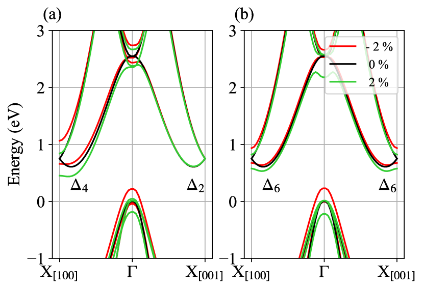
The L valleys, initially 4-fold degenerated, are split into two groups: the ones located along [111] and [11] (), and the two others (). A similar analysis can be done for the K valleys that lead to three different pockets (, , and ) when strain is applied. Finally, the analysis for the U valleys is the same as the ones related to the K valleys and is not repeated here.
Before determining the different band gaps and effective masses for each strained structure, we need to precisely calculate the position of the different points when strain is applied.[47, 51] Using very dense grids in reciprocal space around these valleys, we found that the displacement of the points occurs mainly along the longitudinal direction. In the case of a uniaxial strain in the [110] direction, the valleys show almost no displacement while the valleys show a quadratic displacement, as shown in Fig. 4(a).
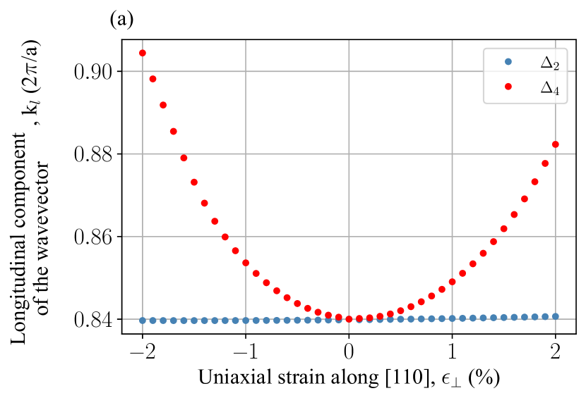
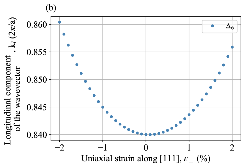
These displacements are taken into account in the following.
The evolution of the band gaps with the uniaxial strain applied along [110] is represented in Fig. 5(a).
The fundamental band gap reduces significantly under both tensile (positive) and compressive (negative) strains, with a sensitivity of eV/% in both cases. However, the indirect band gaps related to the K, U and L valleys all remain larger than 1.91 eV with a maximum strain level of 2%. Therefore, these will not lead to additional contributions to the absorption coefficient in the region of interest, and only the valleys should be considered.
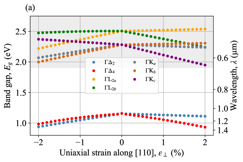
In the case of a uniaxial strain along the [111] direction, the 6-fold degeneracy of the valleys remains, see Fig. 3(b), while the L valley along [111] () is separated from the three others (). For the K and U valleys, there are two different band gaps, namely and . The displacement of the valleys with the applied strain is smaller in this case, see Fig. 4(b). The evolution of the band gaps with the uniaxial strain along the [111] direction is represented in Fig. 5(b). The fundamental band gap also reduces, with a sensitivity of eV/% ( eV/%) for compressive (tensile) strain. The higher-energy and band gaps decrease rapidly with the strain level, but still remain above the considered spectrum. Thus, they will not impact our computed absorption coefficient. Again, only the valleys should be considered.
V.2 Effective masses
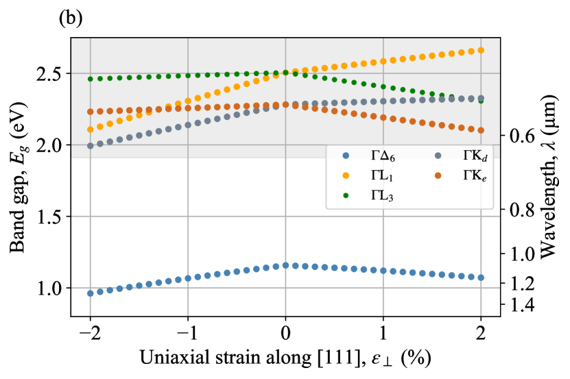
Figure 6 shows the evolution of the conduction band density-of-states effective masses for the different valleys with the applied uniaxial strain.
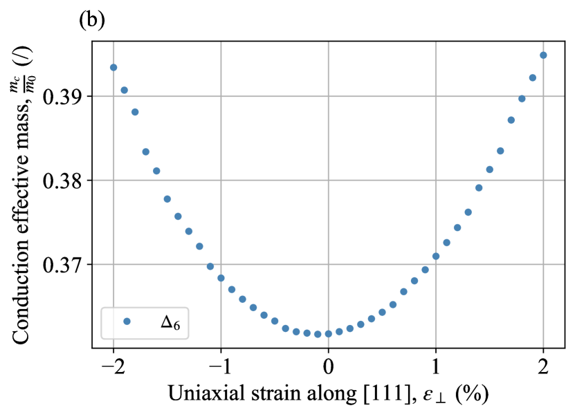
It can be seen that the strain levels considered in this work are not sufficient to affect significantly the conduction band effective masses. As shown later, this effect only slightly impacts the absorption coefficient of highly strained silicon. It can thus safely be ignored.
Figure 7 shows the evolution of the valence band density-of-states effective mass with the applied uniaxial strain.
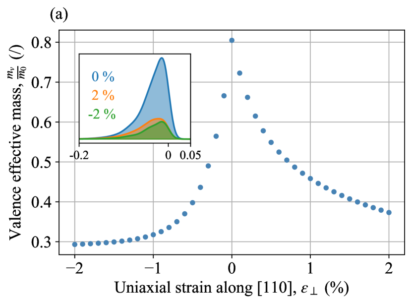
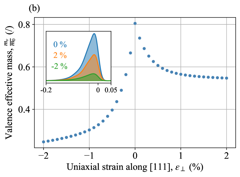
In contrast with the conduction case, the valence band effective mass decreases significantly with the applied strain. This effect is precisely due to the large anisotropy and non-parabolicity of the valence bands, that become more parabolic as strain is applied. The density of states is largely affected, as shown in the insets of Fig. 7, depicting the evolution of the integrand on the right-hand side of Eq. (11) close to the valence band maximum.
V.3 Phonons
The impact of strain on the phonon frequencies must also be carefully analyzed. As explained in Sec. II, only the phonons with a wavevector connecting the valence band maximum at to the conduction band minimum at should be considered. It has recently been shown that the TO, TA and LO modes show a strong electron-phonon coupling for such interband transitions, while the LA mode plays a negligible role.[44] Here, we analyze the behavior of the phonon frequencies for these modes and wavevector . Figure 8 shows the evolution of these with the different types of strain considered, as computed with DFPT.
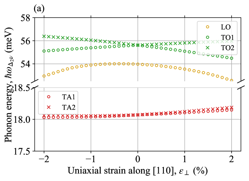
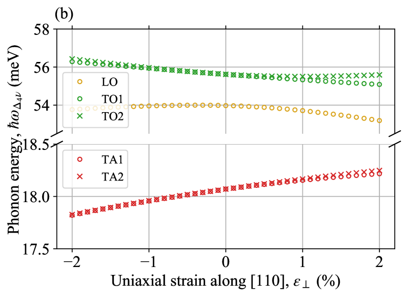
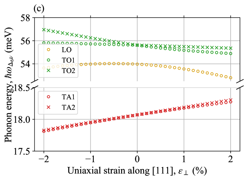
The changes in phonon frequencies are overall negligible, and these changes only have a small impact on the absorption coefficient of highly strained silicon.
The deformation potentials being obtained from the electron-phonon coupling matrix elements,[44] one can make the following assumption. Most of the changes of the electronic structure of silicon due to the strain are related to the value of the band gap, while the character of the conduction band minimum and valence band maximum does not strongly vary. Changes in the band gap do not have a large impact on the electron-phonon coupling matrix elements. The phonon properties are also quite robust with respect to the effect of strain, at least for the strain levels considered in this work. Indeed, the structure only changes by a few percent. For these reasons, we can consider the deformation potentials to be constant with respect to the strain level, as long as the latter remains sufficiently small.
V.4 Indirect absorption
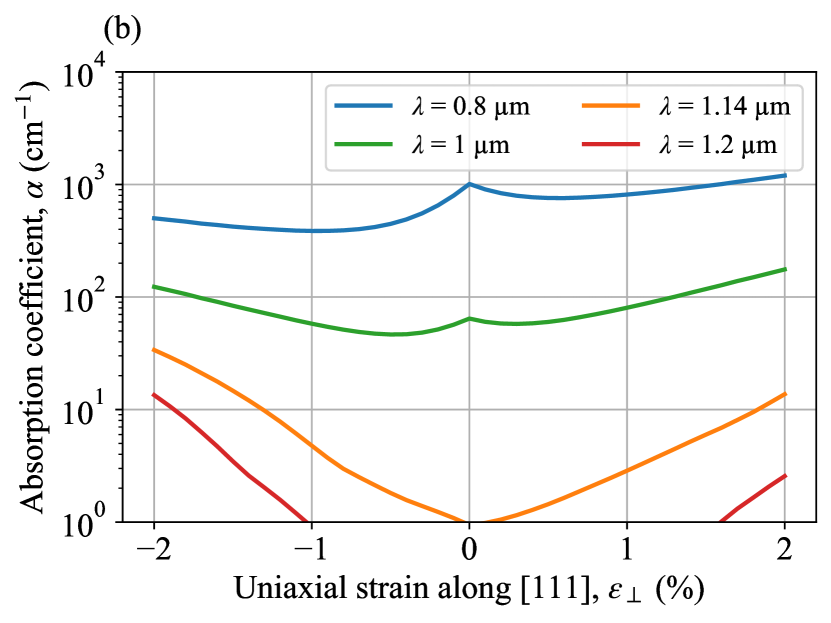
The absorption coefficient of highly strained silicon is shown in Fig. 9.
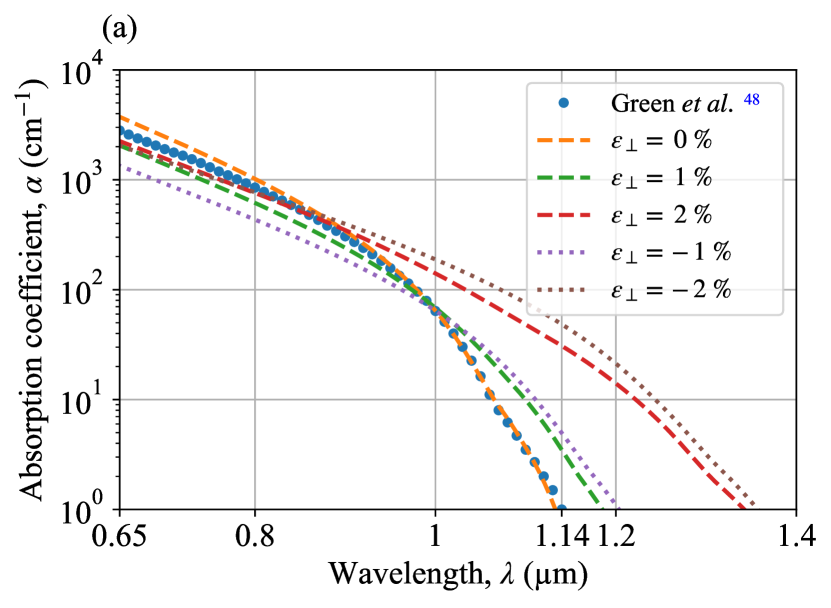
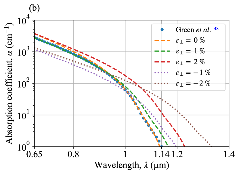
Each valley is considered separately, and their contributions are added up following Eq. (5) and considering the changes in band gaps, effective masses and phonon frequencies due to the strain. Applying uniaxial compressive strain along the [111] direction or tensile and compressive strain along the [110] direction lead to very similar performances. On the other hand, a tensile strain along [111] leads to poorer results, which is related to a smaller reduction of the fundamental band gap, see Fig. 5.
In addition to the shift of the cutoff wavelength, one can see that the absorption coefficient increases by a factor of 15 to 55 at the relaxed cutoff wavelength of 1.14 m, as better shown in Fig. 10 showing the variation of the absorption coefficient with the applied strain, for different wavelengths.
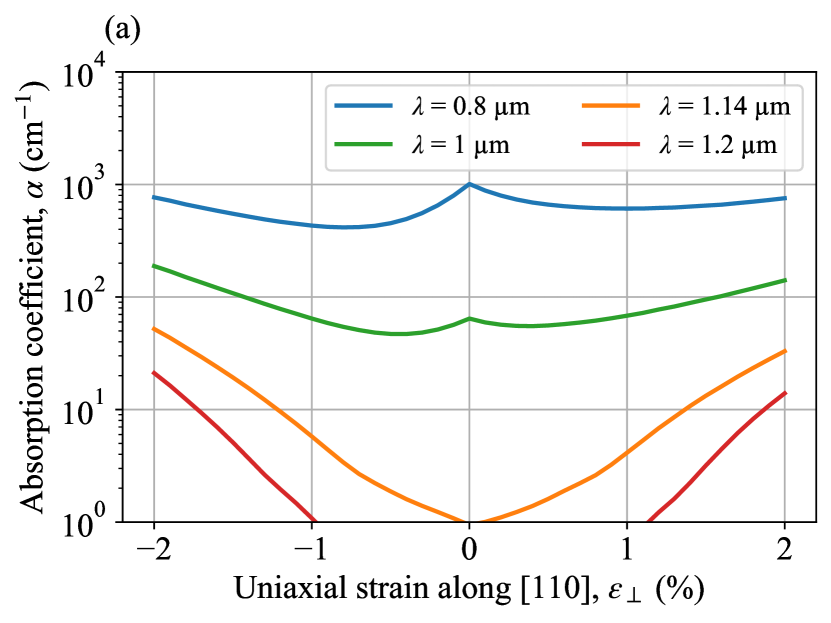
While the absorption coefficient does not show large variations for wavelengths below 1 m, the enhancement is important near the cutoff wavelength (1.14 m). For instance, the absorption coefficient increases by a factor of 55 when a % strain is applied in the [110] direction. The efficiency of a device detecting infrared photons would therefore be greatly enhanced, demonstrating the interest for highly strained silicon for infrared applications.
Another important impact of strain, besides the increased absorption in the infrared, is the shift of the cutoff wavelength towards higher wavelengths, as shown more precisely in Fig. 11.
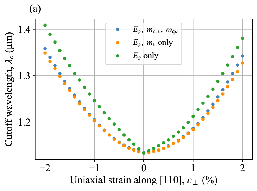
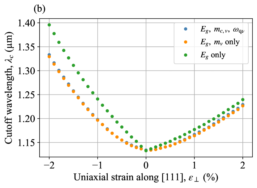
The changes due to the most important parameters are shown in this figure. Considering only the variation of the band gaps (in green) leads to an overestimation of the cutoff wavelength. A result very close to the one calculated with all the parameters changing (in blue) can be obtained by considering the variation of the valence band effective mass in addition to the band gaps (in orange). The impact of the changes in the conduction band effective masses and in phonon frequencies are negligible for most practical applications. We infer that, for a given strain tensor, it is sufficient to compute the relevant band gaps and valence band effective mass of strained silicon to determine its absorption coefficient at a very affordable computational cost.
VI Conclusion
In this work, we have adapted the model developed by Tsai[28] to compute the absorption coefficient of highly strained silicon. Considering uniaxial strain along two directions, [110] and [111], we have computed the relevant material parameters for different strain levels up to %. This has allowed us to identify the band gap as the most important parameter changing with strain, directly followed by the valence band density-of-states effective mass. In contrast, the conduction band density-of-states effective masses and the phonon energies play a minor role in the absorption change. We have shown that highly strained silicon can be used to extend the material bandwidth from 1.14 to 1.35 m. Moreover, the absorption coefficient increases by a factor of 55 at the relaxed cutoff wavelength under a % strain in the [110] direction. We have shown that the impact of strain is mainly significant around the cutoff wavelength which makes strain engineering particularly interesting for infrared applications. This model can be used in conjunction with DFT computations of the relevant band gaps and of the valence band effective mass to determine the absorption coefficient of highly strained silicon in any configuration, at a very limited computational cost compared with fully first-principles electron-phonon computations.
Acknowledgments
G.-M.R. and G.B. are grateful to the F.R.S.-FNRS (Belgium) and to the Communauté française de Belgique through the SURFASCOPE project (ARC 19/24-102) for financial support.
Computational resources have been provided by the supercomputing facilities of the Université catholique de Louvain (CISM/UCL) and the Consortium des Équipements de Calcul Intensif en Fédération Wallonie Bruxelles (CÉCI) funded by the Fond de la Recherche Scientifique de Belgique (F.R.S.-FNRS) under convention 2.5020.11 and by the Walloon Region.
Credit Lines
This article may be downloaded for personal use only. Any other use requires prior permission of the author and AIP Publishing. This article may be found at https://aip.scitation.org/doi/10.1063/5.0057350.
Data Availability
The data that supports the findings of this study are available within the article.
References
- Licht, Peiró, and Villalba [2015] C. Licht, L. T. Peiró, and G. Villalba, “Global substance flow analysis of gallium, germanium, and indium: Quantification of extraction, uses, and dissipative losses within their anthropogenic cycles,” Journal of Industrial Ecology 19, 890–903 (2015), https://onlinelibrary.wiley.com/doi/pdf/10.1111/jiec.12287 .
- Warnock [2011] J. Warnock, “Circuit design challenges at the 14nm technology node,” in Proceedings of the 48th Design Automation Conference (2011) pp. 464–467.
- Waldrop [2016] M. M. Waldrop, “More than moore,” Nature 530, 144–148 (2016).
- Jaeger and Suhling [2018] R. C. Jaeger and J. C. Suhling, “First and second order piezoresistive characteristics of cmos fets: Weak through strong inversion,” in 2018 48th European Solid-State Device Research Conference (ESSDERC) (IEEE, 2018) pp. 126–129.
- Heremans et al. [2016] P. Heremans, A. K. Tripathi, A. de Jamblinne de Meux, E. C. Smits, B. Hou, G. Pourtois, and G. H. Gelinck, “Mechanical and electronic properties of thin-film transistors on plastic, and their integration in flexible electronic applications,” Advanced Materials 28, 4266–4282 (2016).
- Reiche et al. [2009] M. Reiche, O. Moutanabbir, J. Hoentschel, U. Gösele, S. Flachowsky, and M. Horstmann, “Strained Silicon Devices,” Solid State Phenomena 156-158, 61–68 (2009).
- Gnanachchelvi et al. [2016] P. Gnanachchelvi, R. Jaeger, B. Wilamowski, G. Niu, S. Hussain, J. Suhling, and M. Hamilton, “Performance enhancement in bipolar junction transistors using uniaxial stress on (100) silicon,” IEEE Transactions on Electron Devices 63, 2643–2649 (2016).
- Thompson et al. [2006] S. Thompson, S. Suthram, Y. Sun, G. Sun, S. Parthasarathy, M. Chu, and T. Nishida, “Future of strained si/semiconductors in nanoscale mosfets,” in 2006 International Electron Devices Meeting (IEEE, 2006) pp. 1–4.
- Kleimann et al. [1998] P. Kleimann, B. Semmache, M. Le Berre, and D. Barbier, “Stress-dependent hole effective masses and piezoresistive properties of p-type monocrystalline and polycrystalline silicon,” Physical Review B 57, 8966 (1998).
- Nielsen and Martin [1985] O. Nielsen and R. M. Martin, “Stresses in semiconductors: Ab initio calculations on si, ge, and gaas,” Physical Review B 32, 3792 (1985).
- Rieger and Vogl [1993] M. M. Rieger and P. Vogl, “Electronic-band parameters in strained si 1- x ge x alloys on si 1- y ge y substrates,” Physical Review B 48, 14276 (1993).
- Goroff and Kleinman [1963] I. Goroff and L. Kleinman, “Deformation potentials in silicon. iii. effects of a general strain on conduction and valence levels,” Physical Review 132, 1080 (1963).
- Passi et al. [2012] V. Passi, U. Bhaskar, T. Pardoen, U. Sodervall, B. Nilsson, G. Petersson, M. Hagberg, and J.-P. Raskin, “High-throughput on-chip large deformation of silicon nanoribbons and nanowires,” Journal of Microelectromechanical Systems 21, 822–829 (2012).
- Bhaskar et al. [2012] U. Bhaskar, V. Passi, S. Houri, E. Escobedo-Cousin, S. H. Olsen, T. Pardoen, and J.-P. Raskin, “On-chip tensile testing of nanoscale silicon free-standing beams,” Journal of Materials Research 27, 571–579 (2012).
- Kumar Bhaskar et al. [2013] U. Kumar Bhaskar, T. Pardoen, V. Passi, and J.-P. Raskin, “Piezoresistance of nano-scale silicon up to 2 GPa in tension,” Applied Physics Letters 102, 031911 (2013).
- Zhang et al. [2016] H. Zhang, J. Tersoff, S. Xu, H. Chen, Q. Zhang, K. Zhang, Y. Yang, C.-S. Lee, K.-N. Tu, J. Li, et al., “Approaching the ideal elastic strain limit in silicon nanowires,” Science Advances 2, e1501382 (2016).
- Cavallo and Lagally [2012] F. Cavallo and M. G. Lagally, “Semiconductor nanomembranes: A platform for new properties via strain engineering,” Nanoscale Research Letters 7, 1–10 (2012).
- Montmeat et al. [2016] P. Montmeat, I. De Nigris Brandolisi, S. Tardif, T. Enot, G. Enyedi, R. Kachtouli, P. Besson, F. Rieutord, and F. Fournel, “Transfer of Ultra-Thin Semi-Conductor Films onto Flexible Substrates,” ECS Transactions 75, 247–252 (2016).
- Munguía et al. [2008] J. Munguía, G. Bremond, J. Bluet, J. Hartmann, and M. Mermoux, “Strain dependence of indirect band gap for strained silicon on insulator wafers,” Applied Physics Letters 93, 102101 (2008).
- Lange et al. [2016] D. Lange, P. R. i Cabarrocas, N. Triantafyllidis, and D. Daineka, “Piezoresistivity of thin film semiconductors with application to thin film silicon solar cells,” Solar Energy Materials and Solar Cells 145, 93–103 (2016).
- Schriever and Wehrspohn [2012] C. Schriever and R. B. Wehrspohn, “Stretching silicon’s potential,” Nature Materials 11, 96–97 (2012).
- Cazzanelli et al. [2012] M. Cazzanelli, F. Bianco, E. Borga, G. Pucker, M. Ghulinyan, E. Degoli, E. Luppi, V. Véniard, S. Ossicini, D. Modotto, et al., “Second-harmonic generation in silicon waveguides strained by silicon nitride,” Nature Materials 11, 148–154 (2012).
- Fischetti and Laux [1996] M. V. Fischetti and S. E. Laux, “Band structure, deformation potentials, and carrier mobility in strained si, ge, and sige alloys,” Journal of Applied Physics 80, 2234–2252 (1996).
- Wen and Bellotti [2015] H. Wen and E. Bellotti, “Rigorous theory of the radiative and gain characteristics of silicon and germanium lasing media,” Physical Review B 91, 035307 (2015).
- Lin et al. [2017] H. Lin, Z. Luo, T. Gu, L. C. Kimerling, K. Wada, A. Agarwal, and J. Hu, “Mid-infrared integrated photonics on silicon: a perspective,” Nanophotonics 7, 393–420 (2017).
- Noffsinger et al. [2012] J. Noffsinger, E. Kioupakis, C. G. Van de Walle, S. G. Louie, and M. L. Cohen, “Phonon-assisted optical absorption in silicon from first principles,” Physical Review Letters 108, 167402 (2012).
- Zacharias, Patrick, and Giustino [2015] M. Zacharias, C. E. Patrick, and F. Giustino, “Stochastic approach to phonon-assisted optical absorption,” Physical Review Letters 115, 177401 (2015).
- Tsai [2018] C.-Y. Tsai, “Absorption coefficients of silicon: A theoretical treatment,” Journal of Applied Physics 123, 183103 (2018).
- Patrick and Giustino [2014] C. E. Patrick and F. Giustino, “Unified theory of electron–phonon renormalization and phonon-assisted optical absorption,” Journal of Physics: Condensed Matter 26, 365503 (2014).
- Giustino [2017] F. Giustino, “Electron-phonon interactions from first principles,” Reviews of Modern Physics 89, 015003 (2017).
- Pankove [1975] J. I. Pankove, Optical processes in semiconductors (Courier Corporation, 1975).
- Rajkanan, Singh, and Shewchun [1979] K. Rajkanan, R. Singh, and J. Shewchun, “Absorption coefficient of silicon for solar cell calculations,” Solid-State Electronics 22, 793–795 (1979).
- Madelung [1991] O. Madelung, Semiconductors: group IV elements and III-V compounds (Springer, Berlin, Heidelberg, 1991).
- Gonze et al. [2020] X. Gonze, B. Amadon, G. Antonius, F. Arnardi, L. Baguet, J.-M. Beuken, J. Bieder, F. Bottin, J. Bouchet, E. Bousquet, et al., “The abinit project: Impact, environment and recent developments,” Computer Physics Communications 248, 107042 (2020).
- Romero et al. [2020] A. H. Romero, D. C. Allan, B. Amadon, G. Antonius, T. Applencourt, L. Baguet, J. Bieder, F. Bottin, J. Bouchet, E. Bousquet, et al., “Abinit: Overview and focus on selected capabilities,” The Journal of chemical physics 152, 124102 (2020).
- Van Setten et al. [2018] M. Van Setten, M. Giantomassi, E. Bousquet, M. J. Verstraete, D. R. Hamann, X. Gonze, and G.-M. Rignanese, “The pseudodojo: Training and grading a 85 element optimized norm-conserving pseudopotential table,” Computer Physics Communications 226, 39–54 (2018).
- Monkhorst and Pack [1976] H. J. Monkhorst and J. D. Pack, “Special points for brillouin-zone integrations,” Physical Review B 13, 5188 (1976).
- Gonze and Lee [1997] X. Gonze and C. Lee, “Dynamical matrices, born effective charges, dielectric permittivity tensors, and interatomic force constants from density-functional perturbation theory,” Physical Review B 55, 10355 (1997).
- Gonze [1997] X. Gonze, “First-principles responses of solids to atomic displacements and homogeneous electric fields: Implementation of a conjugate-gradient algorithm,” Physical Review B 55, 10337 (1997).
- Trimarchi et al. [2011] G. Trimarchi, H. Peng, J. Im, A. J. Freeman, V. Cloet, A. Raw, K. R. Poeppelmeier, K. Biswas, S. Lany, and A. Zunger, “Using design principles to systematically plan the synthesis of hole-conducting transparent oxides: Cu 3 vo 4 and ag 3 vo 4 as a case study,” Physical Review B 84, 165116 (2011).
- Grosso and Pastori Parravicini [2000] G. Grosso and G. Pastori Parravicini, Solid State Physics, 1st ed. (Academic Press, New York, 2000).
- Green [1990] M. A. Green, “Intrinsic concentration, effective densities of states, and effective mass in silicon,” Journal of Applied Physics 67, 2944–2954 (1990).
- Ridley [1990] B. K. Ridley, Quantum processes in semiconductors, 4th ed. (Oxford University Press, 1990).
- Vandenberghe and Fischetti [2015] W. G. Vandenberghe and M. V. Fischetti, “Deformation potentials for band-to-band tunneling in silicon and germanium from first principles,” Applied Physics Letters 106, 013505 (2015).
- Barber [1967] H. Barber, “Effective mass and intrinsic concentration in silicon,” Solid-State Electronics 10, 1039–1051 (1967).
- Ramos et al. [2001] L. E. Ramos, L. K. Teles, L. M. Scolfaro, J. L. Castineira, A. Rosa, and J. R. Leite, “Structural, electronic, and effective-mass properties of silicon and zinc-blende group-iii nitride semiconductor compounds,” Physical Review B 63, 165210 (2001).
- Bouhassoune and Schindlmayr [2010] M. Bouhassoune and A. Schindlmayr, “Electronic structure and effective masses in strained silicon,” Physica Status Solidi (c) 7, 460–463 (2010).
- Green and Keevers [1995] M. A. Green and M. J. Keevers, “Optical properties of intrinsic silicon at 300 k,” Progress in Photovoltaics: Research and Applications 3, 189–192 (1995).
- Kane [1966] E. Kane, “Band structure of silicon from an adjusted heine-abarenkov calculation,” Physical Review 146, 558 (1966).
- Hybertsen and Louie [1986] M. S. Hybertsen and S. G. Louie, “Electron correlation in semiconductors and insulators: Band gaps and quasiparticle energies,” Physical Review B 34, 5390 (1986).
- Bouhassoune and Schindlmayr [2015] M. Bouhassoune and A. Schindlmayr, “Ab initio study of strain effects on the quasiparticle bands and effective masses in silicon,” Advances in condensed matter physics 2015, 453125 (2015).