Quenching the band gap of 2D semiconductors with a perpendicular electric field
The electronic band structure of atomically thin semiconductors can be tuned by the application of a perpendicular electric field. The principle was demonstrated experimentally shortly after the discovery of graphene by opening a finite band gap in graphene bilayersoostinga_gate-induced_2008 ; zhang_direct_2009 ; mak_observation_2009 , which naturally are zero-gap semiconductors. So far, however, the same principle could not be employed to control a broader class of materials, because the required electric fields are beyond reach in current devices. To overcome this limitation, we have realized double ionic gated transistors that enable the application of very large electric fields. Using these devices, we show that the band gap of few-layer semiconducting transition metal dichalcogenides can be continuously suppressed from 1.5 eV to zero. Our results illustrate an unprecedented level of control of the band structures of 2D semiconductors, which is important for future research and applications.
An electric field applied perpendicular to the surface of a bulk semiconductor is screened over a finite length, leaving the material interior unaffected. In atomically thin semiconductors novoselov_two-dimensional_2005-1 , however, the small thickness prevents efficient screening, so that a perpendicular electric field uniformly influences the entire system, modifying its band structureramasubramaniam_tunable_2011-1 ; drummond_electrically_2012 ; chu_electrically_2015 ; kim_observation_2015 ; dai_bandstructure_2015 ; deng_efficient_2017 ; overweg_electrostatically_2018 . Indeed, a zero-gap semiconductor such as bilayer graphene can be turned into a gapped insulator using double-gated transistors to apply a perpendicular electric fieldoostinga_gate-induced_2008 ; zhang_direct_2009 ; mak_observation_2009 . Despite representing a true conceptual breakthrough, continuous control of the band structure in transistors has not found widespread use, because the limited maximum electric field that can be applied in common devices does not allow significant changes to be induced in most 2D materials.
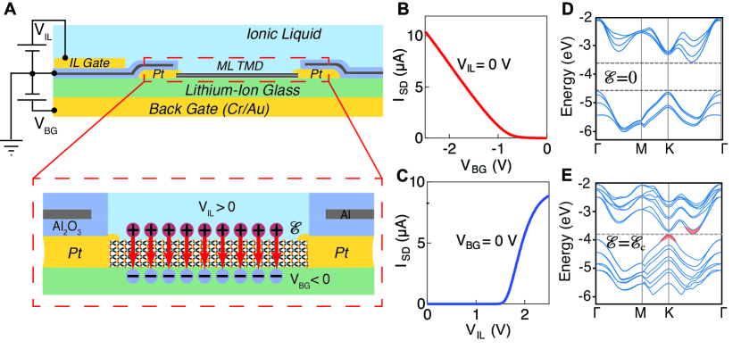
Here we demonstrate the ability to fully quench band gaps as large as 1.5 eV using a new type of transistors based on double ionic gates. Ionic gating relies on electrolytes to transfer the potential from a metallic gate to the surface of a semiconductorfujimoto_electric-double-layer_2013 ; schmidt_characterization_2016 ; bisri_endeavor_2017 . In our devices, two electrolytes in contact with two independent gate electrodes are coupled to a same atomically thin semiconductor (see Fig. 1A). The top electrolyte is a commonly used ionic liquidfujimoto_electric-double-layer_2013 ; schmidt_characterization_2016 ; bisri_endeavor_2017 ; zhang_band_2019 ; gutierrez-lezama_ionic_2021 , and the bottom one is a Li-ion glass ceramic substratephilippi_lithium-ion_2018 ; alam_lithium-ion_2020 . The atomically thin semiconductor is also connected to two metal electrodes functioning as source and drain contacts, and surrounded by a ground plane (an Aluminum film sandwiched between two layers) to eliminate any direct electrostatic coupling of the top and bottom electrolyte (See Supplementary Note S1 for details on device fabrication and S3 for the decoupling of the gates). The use of single ionic gate devices to accumulate charge densities unattainable with conventional gating is by now establishedye_superconducting_2012 ; wang_hopping_2012 ; fujimoto_electric-double-layer_2013 ; lu_evidence_2015 ; costanzo_gate-induced_2016 ; bisri_endeavor_2017 ; leighton_electrolyte-based_2019-1 . However, double ionic gate devices to control independently accumulated charge and electric field have never been reported earlier.
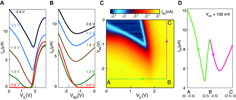
When grounding one of the gates and sweeping the voltage applied to the other, these double gate devices function as conventional transistors, as illustrated by the transfer curves ( measured as a function of gate voltage) recorded on a representative WSe2 tetra-layer (4L) device (see Fig. 1B and 1C; for additional characterization measurements, see Supplementary Note S2). Simultaneously applying a positive voltage to the ionic liquid gate and a negative voltage to the back gate also enables a perpendicular electric field to be established with no net charge accumulated on the semiconductor. To investigate the effect of the perpendicular electric field on the band structure, we look at how the transfer curves -vs- of our device evolve for increasing negative values (Fig. 2A).
For = -0.8 V, the device transfer curve is qualitatively identical to that measured for = 0 V (Fig. 1C): the current increases as is swept past the threshold for electron accumulation ( = 1.7 V), and no current flows for < 1.7 V, when the chemical potential is in the gap. At -1 V, however, the transfer curve exhibits clear qualitative differences, as the current flows even for well below 1.7 V. As is further increased to more negative values, the source-drain current remains large for all values of , without ever vanishing (with a square resistance for all ). Analogous considerations hold true when looking at the evolution of the -vs- transfer curve upon applying a positive voltage to the ionic liquid gate.
The complete evolution of as a function of and is illustrated by the color plot in Fig. 2C. The observed behavior is not the one expected if the only effect of the gate voltages was to affect the electrostatic potential in the transistor channel, i.e., the mechanism that determines the operation of a conventional transistor. In that case, both and would just shift the energy of the 4L-WSe2 bands, and a change in the voltage applied to one of the gates would only cause a rigid shift in the transfer curve measured as a function of the voltage applied to the other gate. The data, however, do not show a rigid shift. That is because the concomitant application of large positive and large negative also generates a perpendicular electric field that quenches the band gap, in agreement with previous theoretical calculationsramasubramaniam_tunable_2011-1 ; dai_bandstructure_2015 and our own (see Fig. 1D and 1E and Supplementary Note S7).
To understand, we look at the evolution of transport as and are varied continuously along the contour outlined by the colored line in Fig. 2C. At point A, and = -2.5 V. The negative potential results in the accumulation of holes (see Fig. 1B), and sets the chemical potential in the WSe2 valence band (the square resistance is 8 k, Fig. 2B). As is increased from 0 to 2.5 V at fixed = -2.5 V, we travel from points A to B (green line). Since the capacitance of the ionic liquid and of the Li-ion glass gates are the same to a very good approximation, the electrostatic potential applied to the channel is proportional to = +, and goes back to zero at B. Nevertheless, the current remains large. If then is decreased from -2.5 to 0 V at fixed = 2.5 V we move from B to C (purple line), where transport is mediated by electrons accumulated by the large positive voltage (see Fig. 1C). Transport therefore evolves from being mediated by holes at point A (with the chemical potential in the valence band), to being mediated by electrons at point C (with the chemical potential in the conduction band), without ever passing through a highly insulating state (see Fig. 2D). This is possible only if the gap closes and the conduction and valence band overlap in some part of the contour, with electrons and holes coexisting in the transistor channel. Indeed, this happens in the neighborhood of B, where the electric field perpendicular to the 4L-WSe2–proportional to = ( - )– is maximum.
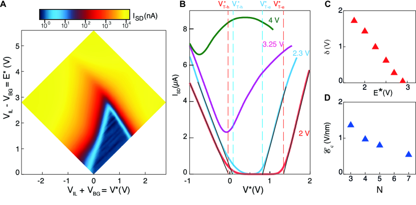
For a quantitative analysis, we plot the current as a function of + and - (Fig. 3A). Fig. 3B shows -vs- curves measured at fixed values of . At small , is finite for sufficiently large negative and positive –with current mediated by holes and electrons respectively– and vanishes over an extended interval, as the chemical potential in 4L-WSe2 is swept across the gap. This interval shrinks as increases, and for > , no highly resistive state is observed, indicating that under these conditions no gap is present. To determine , we extract the threshold voltages for electron and hole conduction ( and ), plot the difference as a function of , and look at when vanishes (Fig. 3C). The corresponding electric field is then approximately given by V/nm, where = 2.6 nm is the thickness of 4L-WSe2. This is a slight overestimate, because part of the voltage drops across the screening length of the two electrolytes. However, as we discuss in detail in Supplementary Note S5, the very large capacitance of the gate electrolytes ( yuan_high-density_2009 ; fujimoto_electric-double-layer_2013 ; schmidt_characterization_2016 ; philippi_lithium-ion_2018 ; zhang_band_2019 ) ensures that the voltage drop across the electrolytes is small, only approximately 10 %, from which we conclude that the electric field needed to quench the gap of 4L WSe2 is between 0.9 and 1.0 V/nm (note that this is the actual electric field, and not the displacement field, which is frequently referred to in the literature when analyzing experiments on double-gated transistors). We have performed similar experiments also on 3L, 5L and 7L WSe2 and succeeded in closing the band gap in all cases (see Supplementary Note S6 for data measured on devices of different thickness). The required electric fields are plotted in Fig. 3D.
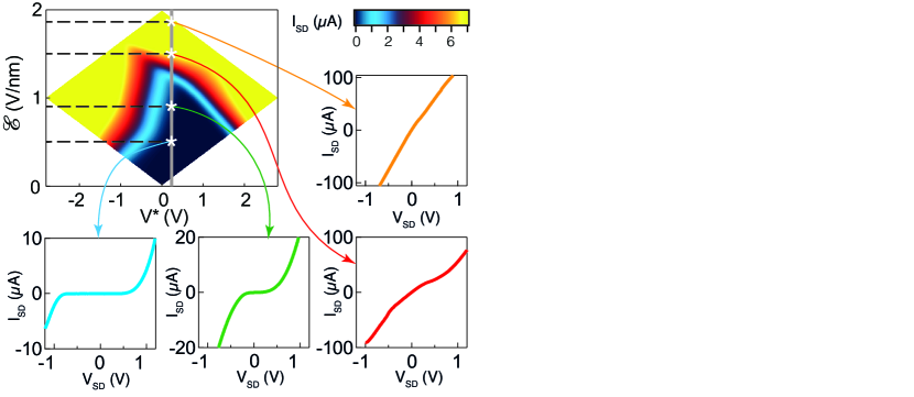
The evolution of the -vs- curves upon increasing the perpendicular electric field confirms that the gap closes (see Fig. 4). At = 0, a pronounced suppression of over a broad range is observed when the 4L-WSe2 device is biased at = + = 0.2 V, corresponding –for = 0 V– to setting the chemical potential well inside the gap. Upon increasing (with fixed), the suppression becomes less pronounced and eventually the -vs- curve becomes perfectly linear. That is what happens after the gap has closed, when the overlap of valence and conduction band is sufficiently large.
Within the precision of both theory and experiments, the value of electric field needed to quench the gap of few-layer WSe2 is in agreement with expectations (See Supplementary Note S7). In qualitative terms, the gap closes when the electrostatic potential is sufficient to lift the energy of the valence band edge at one crystal surface above the conduction band edge at the opposite surface, so that the conduction and valence band overlap, and the system becomes gapless. This conclusion holds true for all semiconductors, but the nature of the gapless state depends on details. For sufficiently thin crystals –such as 4L-WSe2– the electron and hole wavefunctions at opposite surfaces are expected to overlap in space and hybridize. In this regime, the appearance of topological states has been predicted in semiconducting transition metal dichalcogenidesqian_quantum_2014 ; tong_topological_2017 ; zhu_gate_2019 . For thicker crystals hybridization eventually becomes negligible, and the electron and hole accumulation layers on opposite surfaces only couple through Coulomb interaction. Closing the gap of atomically thin semiconductors with a perpendicular electric field therefore leads to the formation of electron-hole systems that have not been realized earlier.
Tuning the gap continuously –and suppressing it altogether– discloses the possibility to control virtually all aspects of the physics of a semiconductor, including its emission and absorption spectrum, as well as other optical and transport properties. As such, the electrostatic control of the band gap opens new routes for the realization of technologically relevant photonic devices. Examples are broadly tunable light sourcesjauregui_electrical_2019 , possibly covering energy ranges in which achieving light emission is traditionally difficult (e.g., in the very far infrared), or optical modulators. We therefore anticipate that the results presented here will attract interest in the fields of optoelectronics and optical communications.
Data availability
The data that support the findings of this study are available from the corresponding author without any restriction.
Author contributions
D.D., M.P., N.U., and I.G.L. fabricated the devices and carried out the experiments. D.D, M.P., I.G.L, and A.F.M. analysed the experimental data. M.G. performed first-principles simulations. I.G.L. supervised the experimental work and A.F.M. conceived and directed the research. All authors participated in preparing the manuscript.
acknowledgements
The authors thank A. Ferreira for technical support. A.F.M. acknowledges financial support from the Swiss National Science Foundation (Division II) and from the EU Graphene Flagship project. M.G. acknowledges support from the Italian Ministry for University and Research through the Levi-Montalcini program.
Competing interests
The authors declare no competing interests.
References
- (1) Oostinga, J. B., Heersche, H. B., Liu, X., Morpurgo, A. F. & Vandersypen, L. M. K. Gate-induced insulating state in bilayer graphene devices. Nature Materials 7, 151–157 (2008).
- (2) Zhang, Y. et al. Direct observation of a widely tunable bandgap in bilayer graphene. Nature 459, 820–823 (2009).
- (3) Mak, K. F., Lui, C. H., Shan, J. & Heinz, T. F. Observation of an Electric-Field-Induced Band Gap in Bilayer Graphene by Infrared Spectroscopy. Phys. Rev. Lett. 102, 256405 (2009).
- (4) Novoselov, K. S. et al. Two-dimensional atomic crystals. PNAS 102, 10451–10453 (2005).
- (5) Ramasubramaniam, A., Naveh, D. & Towe, E. Tunable band gaps in bilayer transition-metal dichalcogenides. Physical Review B 84, 205325 (2011).
- (6) Drummond, N. D., Zólyomi, V. & Fal’ko, V. I. Electrically tunable band gap in silicene. Physical Review B 85, 075423 (2012).
- (7) Chu, T., Ilatikhameneh, H., Klimeck, G., Rahman, R. & Chen, Z. Electrically Tunable Bandgaps in Bilayer MoS2. Nano Letters 15, 8000–8007 (2015).
- (8) Kim, J. et al. Observation of tunable band gap and anisotropic Dirac semimetal state in black phosphorus. Science 349, 723–726 (2015).
- (9) Dai, X., Li, W., Wang, T., Wang, X. & Zhai, C. Bandstructure modulation of two-dimensional WSe2 by electric field. Journal of Applied Physics 117, 084310 (2015).
- (10) Deng, B. et al. Efficient electrical control of thin-film black phosphorus bandgap. Nature Communications 8, 14474 (2017).
- (11) Overweg, H. et al. Electrostatically Induced Quantum Point Contacts in Bilayer Graphene. Nano Letters 18, 553–559 (2018).
- (12) Fujimoto, T. & Awaga, K. Electric-double-layer field-effect transistors with ionic liquids. Physical Chemistry Chemical Physics 15, 8983–9006 (2013).
- (13) Schmidt, E., Shi, S., Ruden, P. P. & Frisbie, C. D. Characterization of the Electric Double Layer Formation Dynamics of a Metal/Ionic Liquid/Metal Structure. ACS Appl. Mater. Interfaces 8, 14879–14884 (2016).
- (14) Bisri, S. Z., Shimizu, S., Nakano, M. & Iwasa, Y. Endeavor of Iontronics: From Fundamentals to Applications of Ion-Controlled Electronics. Advanced Materials 29, 1607054 (2017).
- (15) Zhang, H., Berthod, C., Berger, H., Giamarchi, T. & Morpurgo, A. F. Band Filling and Cross Quantum Capacitance in Ion-Gated Semiconducting Transition Metal Dichalcogenide Monolayers. Nano Letters 19, 8836–8845 (2019).
- (16) Gutiérrez-Lezama, I., Ubrig, N., Ponomarev, E. & Morpurgo, A. F. Ionic gate spectroscopy of 2D semiconductors. Nature Reviews Physics 1–12 (2021).
- (17) Philippi, M., Gutiérrez-Lezama, I., Ubrig, N. & Morpurgo, A. F. Lithium-ion conducting glass ceramics for electrostatic gating. Applied Physics Letters 113, 033502 (2018).
- (18) Alam, M. H. et al. Lithium-ion electrolytic substrates for sub-1V high-performance transition metal dichalcogenide transistors and amplifiers. Nature Communications 11, 3203 (2020).
- (19) Ye, J. T. et al. Superconducting Dome in a Gate-Tuned Band Insulator. Science 338, 1193–1196 (2012).
- (20) Wang, S., Ha, M., Manno, M., Daniel Frisbie, C. & Leighton, C. Hopping transport and the Hall effect near the insulator–metal transition in electrochemically gated poly(3-hexylthiophene) transistors. Nature Communications 3, 1210 (2012).
- (21) Lu, J. M. et al. Evidence for two-dimensional Ising superconductivity in gated MoS2. Science 350 (2015).
- (22) Costanzo, D., Jo, S., Berger, H. & Morpurgo, A. F. Gate-induced superconductivity in atomically thin MoS crystals. Nature Nanotechnology 11, 339–344 (2016).
- (23) Leighton, C. Electrolyte-based ionic control of functional oxides. Nature Materials 18, 13–18 (2019).
- (24) Yuan, H. et al. High-Density Carrier Accumulation in ZnO Field-Effect Transistors Gated by Electric Double Layers of Ionic Liquids. Advanced Functional Materials 19, 1046–1053 (2009).
- (25) Qian, X., Liu, J., Fu, L. & Li, J. Quantum spin Hall effect in two-dimensional transition metal dichalcogenides. Science 346, 1344–1347 (2014).
- (26) Tong, Q. et al. Topological mosaics in moiré superlattices of van der Waals heterobilayers. Nature Physics 13, 356–362 (2017).
- (27) Zhu, Q., Tu, M. W.-Y., Tong, Q. & Yao, W. Gate tuning from exciton superfluid to quantum anomalous Hall in van der Waals heterobilayer. Science Advances 5, eaau6120 (2019).
- (28) Jauregui, L. A. et al. Electrical control of interlayer exciton dynamics in atomically thin heterostructures. Science 366, 870–875 (2019).