Optical anisotropies of asymmetric double GaAs (001) Quantum Wells
Abstract
In the present work, we were able to identify and characterize a new source of in-plane optical anisotropies (IOAs) occurring in asymmetric DQWs; namely a reduction of the symmetry from to as imposed by asymmetry along the growth direction. We report on reflectance anisotropy spectroscopy (RAS) of double GaAs quantum wells (DQWs) structures coupled by a thin ( nm) tunneling barrier. Two groups of DQWs systems were studied: one where both QWs have the same thickness (symmetric DQW) and another one where they have different thicknesses (asymmetric DQW). RAS measures the IOAs arising from the intermixing of the heavy- and light- holes in the valence band when the symmetry of the DQW system is lowered from to . If the DQW is symmetric, residual IOAs stem from the asymmetry of the QW interfaces; for instance, associated to Ga segregation into the AlGaAs layer during the epitaxial growth process. In the case of an asymmetric DQW with QWs with different thicknesses, the AlGaAs layers (that are sources of anisotropies) are not distributed symmetrically at both sides of the tunneling barrier. Thus, the system losses its inversion symmetry yielding an increase of the RAS strength. The RAS line shapes were compared with reflectance spectra in order to assess the heavy- and light- hole mixing induced by the symmetry breakdown. The energies of the optical transitions were calculated by numerically solving the one-dimensional Schrödinger equation using a finite-differences method. Our results are useful for interpretation of the transitions occurring in both, symmetric and asymmetric DQWs.
I Introduction
Nanostructures based on double quantum wells (DQWs) constitute an excellent platform to study the interactions between confined energy levels; for instance, intra-QW transitions between electrons and holes belonging to the same QW (direct excitons and trions), and inter-QW transitions occurring for electrons and holes resident in different QW (indirect excitons and indirect trions) [1]. The strength of the direct and indirect transitions can be modulated by the application of external perturbations, such as external electric fields. The electric field modifies the tunneling probability leading to the appearance of spatially indirect inter-QW excitons [1, 2, 3] and intra-QW charged excitons (trions) [1]. Such complex band structures offer interesting optical phenomena which exhibit polarization dependence. In-plane optical anisotropies (IOAs) of AlGaAs/GaAs-based heterostructure have been studied extensively in the past several years by means of reflectance anisotropy spectroscopy (RAS). In the case of single QWs, several sources of IOAs have been investigated: i) absence of 4-fold rotational symmetry axis at the AlGaAs/GaAs interface [4, 5], ii) asymmetric quantum wells [6], iii) nonuniform segregation of Ga atoms at AlGaAs/GaAs interfaces [5, 7], iv) application of an external stress [8, 9], and v) asymmetric barriers [10]. In general, the observed IOAs strength depends on the QW thickness. For example, for strain-induced IOAS, the RAS response increases with the well thickness [8, 9]; whereas it decreases with well thickness for the anisotropies induced exclusively by the interfaces [5, 8, 10].
| Sample number | Well width | Well width | |
|---|---|---|---|
| S1 | 11.87 | 11.87 | Si doped, |
| A1 | 13.85 | 11.87 | Si doped, |
| A2 | 23.74 | 11.87 | Si doped, |
| A3 | 23.74 | 11.87 | Be doped, |
In DQW-based systems, the relative thickness of the QWs plays an important role in the anisotropy strength; namely, if both QWs have the same thickness (symmetric DQW), the IOA arises from the contributions of the AlGaAs/GaAs(QW) and GaAs(QW)/AlGaAs interfaces which, in general, are not equivalent. If the QWs thicknesses are different (asymmetric DQW), the system loses its inversion symmetry as a whole along a plane perpendicular to the growth direction an passing through the center of the tunneling barrier; therefore, the interfaces of the DQW system are not distributed symmetrically at both sides of the tunneling barrier, leading to an increase of the IOA signal.
In this paper we report on RAS experiments on DQWs coupled by a thin barrier (1.98 nm) and different relative thicknesses. We find that by increasing the thickness of one of the QWs relative to the other, we induce a breakdown of inversion symmetry of the DQW structure which increases the IOA.
The rest of the paper is organized as follows. In Sec. II, a description of samples and the experimental setup is given. In Sec. III, a description of the numerical model used to calculate the energy of the excitonic transitions of the DQWs and a detailed description of the model used to explain the RAS spectra are discussed. In Sec. IV, we describe the RAS and photoluminescence (PL) on symmetric and asymmetric DQWs as well as their interpretation on the basis of the breakdown of inversion symmetry. Finally, conclusions are given in Sec. V.
II Samples AN EXPERIMENTAL SETUP
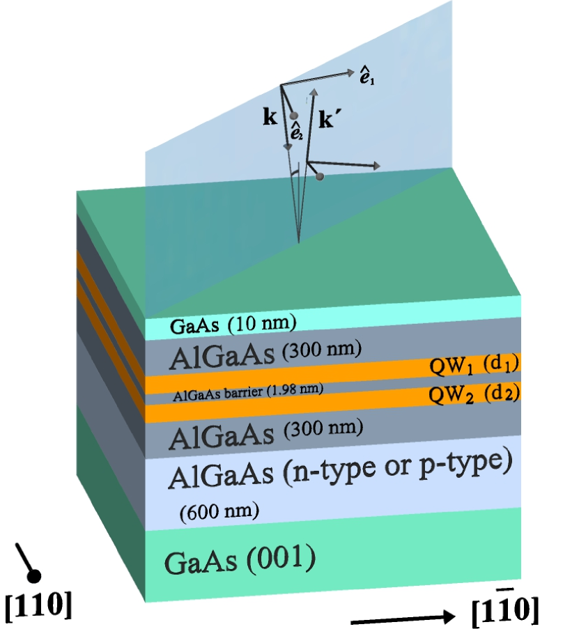
The samples were grown by molecular beam epitaxy (MBE) on a GaAs (001) semi-insulating substrates covered with a 200 nm-thick smooth GaAs buffer layer (see Fig. 1 and Table 1). On top of this layer, a 600 nm-thick, n-type (samples S1, A1, A2) or p-type (sample A3) layer was grown. The DQW consists of two undoped GaAs QWs of thicknesses and separated by a 1.98 nm thick barrier. Sample S1 is a symmetric DQW (i.e., with ) while samples A1, A2 and A3 are asymmetric . The whole structures were covered with a 10 nm-thick GaAs capping layer.
RAS and reflectance (R) experiments were carried out using for excitation the monochromatic probe light obtained by filtering a 70 W tungsten lamp with a monochromator. The monochromatic beam then passes through a polarizer prism and a photo-elastic modulator in tandem and is focused onto the sample with a spot size of 5.0 mm of diameter. The sample is chilled at cryogenic temperatures (30 K) by means of a Helium closed cycle cryocooler. The light reflected by the sample is collected and detected by a multialkali photomultiplier tube. A detailed description of the RAS technique can be found elsewhere [11].
III Model
III.1 Numerical calculations
The one-dimensional Schrödinger equation in the effective mass approach was solved using the finite difference method [12, 13] to obtain both the transition energies and wave functions of the DQWs. We neglect spin-orbit interaction, which leads to a Luttinger’s Hamiltonian [14] with decoupled heavy- and light- hole states. Taking into account the band-edge variation as well as the dependence of the effective mass on the composition of the layers [15, 13, 16, 17], our system can be described by:
| (1) |
The Varshni equation was employed for the determination of gap energies of alloys [18]. The conduction and valence band offsets were chosen as 65% and 35%, respectively. Both electron and hole effective masses for GaAs and AlAs can be found in Refs. [19, 20, 21], whereas for the Vegard’s law was used [22].
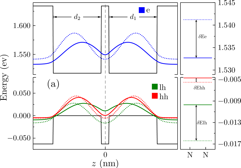
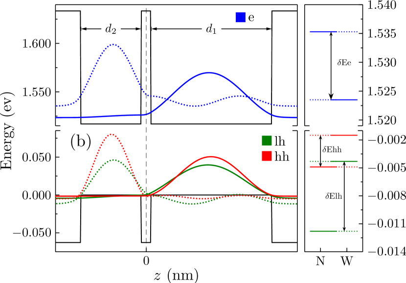
Figure (2) shows the energies and wave functions of the S1 (Fig. 2) and A1 (Fig. 2) samples calculated by the finite difference model without band nonparabolicity. The transition energies were calculated by taking into consideration the exciton binding energy as a function of the well width [23, 16]. We show that wave functions in asymmetric DQW are asymmetrically distributed around the tunneling barrier for both electrons and holes. The barrier width plays an important role in tunneling. For symmetric DQW, as noted above, the electron and heavy- light- holes states are quite similarly localized in the two wells and there is a splitting of the degenerate single states into doublets. For asymmetric DQW the energies of doublets tend to the singlet state energy of a single QW [24].
| Sample | e1-hh1 | e1-lh1 | e2-hh2 | e2-lh2 | e3-hh3 | (meV) | (meV) | (meV) | (meV) |
|---|---|---|---|---|---|---|---|---|---|
| S1 | (E)1.5328 (N)1.5297 | (E)1.5380 (N)1.5341 | (N)1.5394 | (N)1.5499 | (N)1.5948 | 8.9 | 0.9 | 6.9 | |
| A1 | (E)1.5265 (N)1.5273 | (E)1.5296 (N)1.5314 | (N)1.5368 | (N)1.5460 | (N)1.5837 | 8.4 | 1.3 | 6.4 | |
| A2 | (E)1.5181 (N)1.5190 | (E)1.5206 (N)1.5210 | (N)1.5330 | (N)1.5394 | (N)1.5460 | 11.8 | 3.4 | 7.5 |
III.2 Anisotropy Model
GaAs is a cubic crystal of the symmetry group . For a single QW grown on the (001) surface, the direction becomes inequivalent to both and directions, hence lowering symmetry from to . This group comprises eight operations of symmetry including four that changes
the direction of the -axis. In this symmetry group, the and axes remain equivalent and the optical properties are isotropic in the plane. An IOA is expected when the axis loses its 4-fold rotation symmetry, lowering the symmetry further from to . Different perturbations have been considered to increase the IOA; among them we can count on: uniaxial external stress applied along direction, ultra-thin layers inserted in one QWs barrier, and external electric fields applied along the direction.
Another mechanism that induces an IOA in a single QW is the non-equivalence of the AlGaAs/GaAs interfaces. As a matter of fact, in a single QW the anisotropies originated at the AlGaAs/GaAs(QW) and at the GaAs(QW)/AlGaAs interfaces are reversed in sign, thus cancelling the IOA ( symmetry). However, it is well-known, that, experimentally, they are not exactly equivalent from the structural point of view
[9] and a residual IOA is normally observed [4, 5] ( symmetry). RAS
spectra of single QWs have been reported extensively in the literature [5, 6, 8, 9, 10].
The thickness of the QW plays a fundamental role in the amplitude of the RAS signal. For the anisotropies originated at the interfaces and the ones induced by the segregation of Ga or In (in the case of the inclusion of a thin InAs layer), the RAS amplitude decreases when the thickness of the QW increases [5]. Contrary to this behavior, for the IOA induced by strain, the RAS signal increases with the thickness of the QW [8]. In any case, the RAS signal is associated to the mixing between the heavy- and light-hole valence subbands of the QW [25]. In a perturbative approach the IOA strength is proportional to:
| (2) |
where and are the overlap integrals between the electron state in the conduction band and the and hole states in the valence band respectively. The mixing between heavy- and light-hole subbands is being the perturbative Hamiltonian. The difference in energy between the hole states before their mixing is .
As previously mentioned, could account for a perturbation by applied uniaxial stresses, electric fields (built-in or external) and abrupt or smooth interfaces.
In the case of coupled DQW system, is a measure of the asymmetry of the two QWs.
In a DQW, if both QWs have the same thickness, the electron and hole energy levels are brought
into resonance and their probability density is distributed symmetrically at both sides of the barrier that connects both QWs, as can be seen in Fig. 2. If the AlGaAs/GaAs interfaces of the DQW are equivalent the symmetry of the DQW structure belongs to the crystallographic point group. However, as we mentioned, if the GaAs/AlGaAs interfaces (sources of anisotropies) are non-equivalent, and a residual IOA is induced by the symmetry reduction from to of the whole DQW structure. In this case the number of symmetry operations is reduced to four: the operations that inverts the -axis, are excluded, thus leading to a mixing of heavy- and light- holes in the valence band, and hence an IOA.
When the thickness of one QWs is larger than the other QW (asymmetric DQW), the energy of the electron and hole states of each QW become different and are no longer in resonance. In this case, the probability density is distributed asymmetrically as can be seen in Fig. 2. Besides of the anisotropic source induced by the GaAs/AlGaAs interfaces as in the symmetric case, for the asymmetric DQW system another mechanism of IOA should be considered. Suppose that the AlGaAs/GaAs interfaces are equivalent. As we mentioned, in this case a symmetric DQW system belongs to the symmetry. If the thickness of one QW is modified, the system changes symmetry from to . As can be seen in Fig. 2, the symmetry operations that change the sign of the -axis (i.e., a reflection on a plane perpendicular to ), are no longer possible because the AlGaAs/GaAs interfaces are located at different distances from the barrier. The number of symmetry operations of the asymmetric DQW structure is reduced to the four operations of the symmetry group [26, 27]. In this case the IOA strength can be modulated by changing the relative thicknesses of the QWs in the DQW system. This anisotropy is added to the residual IOA produced by the non-equivalence of the interfaces.
IV Experimental Results
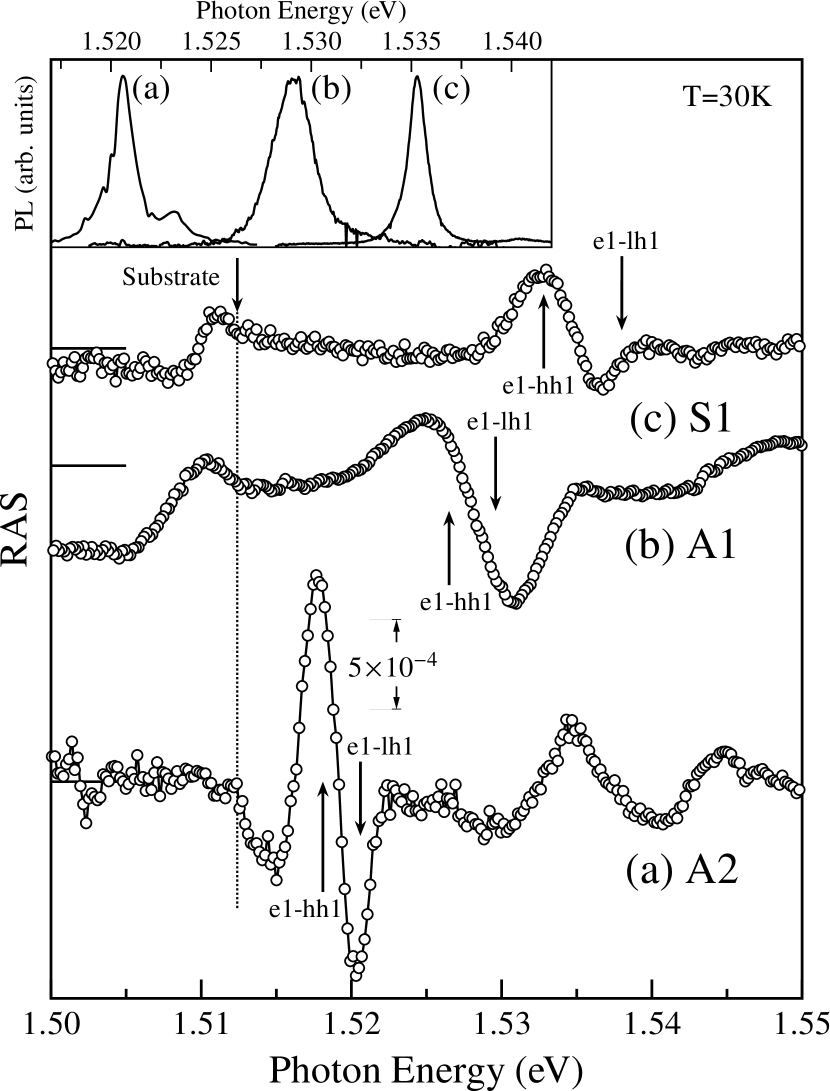
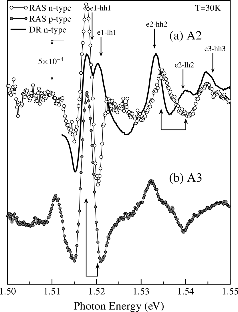
Figure 3 shows the RAS spectra recorded at 30K for the samples S1, A1 and A2 (described in Table 1). The inset plot show the corresponding PL spectra measured at 12K, where the excitonic transitions can be identified by two peaks, the larger one associated with e1-hh1 transition and a much smaller one associated to the e1-hh1. In the case of RAS, the peaks associated with these transitions are seen clearer. The e1-hh1 and e1-lh1 transitions determined in the PL spectra are indicated by arrows. These values are in excellent agreement with those determined by the numerical calculations (see Table 2). Note that the features associated to each transition have opposite concavities and red-shift when one of the QWs of the system increases its thickness. The evolution of the optical structure is evident: if the DQW structure become asymmetric the corresponding RAS spectra increases its strength.
Due to the fact that the wave function probability density of sample is distributed symmetrically along the QWs structure, the IOA strength is expected to be similar to that obtained for a single QW is expected. In fact, a RAS signal of the order of magnitude of has been reported for a 8 nm single QW [5], which has the same order of magnitude as in spectra of Fig. 3(c). This IOA is attributed to the inequivalent AlGaAs/GaAs interfaces along
the DQW structure.
As pointed out before, the strength of the IOA signal is produced by an intermixing of the heavy- and light hole states in the valence band which is proportional to according to Eq. (2). For the lowest heavy and light holes levels (n=1), there is an estimated separation in energy of around = 2.0, 4.1 and 4.4 meV for samples A2 (A3), A1 and S1, respectively. The mixing can be estimated by considering that the transitions are direct (n is the same for the valence and conduction band) and then the overlapping terms in Eq. (2) must be approximately the same for each sample. For transitions n=1 it can be seen in Fig. 3, that the amplitude ratio of the spectra between A2 and A1 with respect to S1 are 1.5 and 3.7 respectively. Thus from Eq. (2) we estimate ratios of for sample A1 and for sample A2.
In order to elucidate the physical origin of the RAS in the asymmetric DQWs, we compare in Fig. 4 the RAS and the DR spectra of the asymmetric sample A2. DR spectra is obtained by the numerical subtraction of the reflection (R) spectra recorded at 30K and 300K followed by the normalization to the 300K spectrum. The subtraction highlights the excitonic features, which are very weak (and energy shifted) at 300K. The comparison between RAS and DR spectra allows us to contrast the contribution of the heavy and light holes transitions. Around 1.5175 eV, the DR spectrum shows two peaks corresponding to e1-hh1 and e1-lh1 transitions. Note that in the RAS spectrum, the structure associated to e1-hh1 transition has the same concavity as the corresponding for the DR spectrum, while the e1-lh1 transition has the opposite concavity. This is an indication of the transfer of oscillator strength between the levels due to the intermixing of heavy- and light- holes, thus supporting our anisotropy model. The same behavior applies for the e2-hh2 and e2-lh2 transitions at around 1.5375 eV. Transition e2-hh3 is also indicated and it has the same concavity for RAS and DR spectra, as in the case of the e1-hh1 and e2-hh2 transitions.
The arrows at the bottom of Fig. 4 indicate the energy of the states en-hhn and en-lhn (for n =1 and 2) obtained from the maximum and minimum of the RAS spectrum. From the numerical calculation results summarized in Table 2, the energy splitting between transitions en-hhn and en-lhn are meV and meV. In accordance with Eq. (2), the IOA amplitude is proportional to . Considering the same valued for the overlapping and the mixing we estimate an amplitude ratio of 3.25 between these transitions. This value is close to the value of 3.9 obtained by the RAS spectrum of Fig. 4 supporting our interpretation.
Finally, we discuss the possible contribution to the RAS amplitude by an built-in electric field accross the DQW. To study this contribution, we have compared the RAS spectra of asymmetric samples A2 and A3. The difference between them is the doping of the AlGaAs layer (see Fig. 1). While for A2 it is n-type, for A3 it is p-type. Assuming that the built-in electric field originates from charge transfer between surface states and the AlGaAs doped layer (n or p), this field is expected to have opposite signs for samples A2 and A3. Thus, the linear contribution of the electric field to the RAS should be reversed in sign for such samples. Figure 4 shows the comparison between the RAS spectra of samples A2 and A3 obtained from the difference in reflectivity between the and crystallographic directions. As can be seen, RAS spectra are equivalent in shape and have the same sign, thus indicating that the contribution of the electric field to the RAS signal is very small. We conclude, thus, that the dominant contribution to RAS spectra is the asymmetry of the DQW system.
V Conclusion
We presented in this work a detailed study of the evolution with QW thickness of the RAS spectra of a coupled DQW system. The RAS signal increases its strength with the degree of asymmetry of the QWs that constitutes the DQW system. This behavior is attributed to the reduction of the symmetry of the electronic states in the DQWs with QWs of different thicknesses. The nature of the transitions was identified by using PL spectroscopy and numerical calculations. We believe that the result presented in this work are important and will be useful in understanding of the evolution of the optical transition induced by the breakdown of translation symmetry in asymmetric DQWs.
VI ACKNOWLEDGMENTS
We would like to thank L. E. Guevara-Macías, E. Ontiveros, F. Ramírez-Jacobo and J. Gonzalez-Fortuna for their skillful technical support. This work was supported by Consejo Nacional de Ciencia y Tecnología (grants FC-2093-2018, CB-256578-2016, CB-30406-2018, CB-252867 and 299552).
References
- Yuan et al. [2018] M. Yuan, A. Hernández-Mínguez, K. Biermann, and P. V. Santos, Tunneling blockade and single-photon emission in gaas double quantum wells, Phys. Rev. B 98, 155311 (2018).
- Miller et al. [1984] D. A. B. Miller, D. S. Chemla, T. C. Damen, A. C. Gossard, W. Wiegmann, T. H. Wood, and C. A. Burrus, Band-edge electroabsorption in quantum well structures: The quantum-confined stark effect, Phys. Rev. Lett. 53, 2173 (1984).
- Chen et al. [1987] Y. J. Chen, E. S. Koteles, B. S. Elman, and C. A. Armiento, Effect of electric fields on excitons in a coupled double-quantum-well structure, Phys. Rev. B 36, 4562 (1987).
- Krebs and Voisin [1996] O. Krebs and P. Voisin, Giant optical anisotropy of semiconductor heterostructures with no common atom and the quantum-confined pockels effect, Phys. Rev. Lett. 77, 1829 (1996).
- Chen et al. [2002] Y. H. Chen, X. L. Ye, J. Z. Wang, Z. G. Wang, and Z. Yang, Interface-related in-plane optical anisotropy in single-quantum-well structures studied by reflectance difference spectroscopy, Phys. Rev. B 66, 195321 (2002).
- Koopmans et al. [1998] B. Koopmans, B. Koopmans, P. Santos, P. Santos, and M. Cardona, Microscopic reflection difference spectroscopy on semiconductor nanostructures, physica status solidi (a) 170, 307 (1998).
- Braun et al. [1997] W. Braun, A. Trampert, L. Däweritz, and K. H. Ploog, Nonuniform segregation of ga at alas/gaas heterointerfaces, Phys. Rev. B 55, 1689 (1997).
- Tang et al. [2009] C. G. Tang, Y. H. Chen, B. Xu, X. L. Ye, and Z. G. Wang, Well-width dependence of in-plane optical anisotropy in (001) gaas/algaas quantum wells induced by in-plane uniaxial strain and interface asymmetry, Journal of Applied Physics 105, 103108 (2009).
- Li et al. [2019] Y. Li, F. Liu, X. Ye, Y. Liu, J. Wang, and Y. Chen, Quantitative investigation of intrinsic shear strain and asymmetric interface conditions in semiconductor superlattices, Journal of Applied Physics 126, 065704 (2019).
- Yu et al. [2015] J. L. Yu, S. Y. Cheng, Y. F. Lai, Q. Zheng, Y. H. Chen, and C. G. Tang, Tuning of in-plane optical anisotropy by inserting ultra-thin inas layer at interfaces in (001)-grown gaas/algaas quantum wells, Journal of Applied Physics 117, 015302 (2015).
- Lastras‐Martínez et al. [1993] L. F. Lastras‐Martínez, A. Lastras‐Martínez, and R. E. Balderas‐Navarro, A spectrometer for the measurement of reflectance‐difference spectra, Review of Scientific Instruments 64, 2147 (1993).
- [12] Numerical solutions, in Quantum Wells, Wires and Dots (John Wiley & Sons, Ltd) Chap. 3, pp. 81–130.
- Hamaguchi [2017] C. Hamaguchi, Basic Semiconductor Physics (Springer International Publishing, 2017).
- Luttinger [1956] J. M. Luttinger, Quantum theory of cyclotron resonance in semiconductors: General theory, Phys. Rev. 102, 1030 (1956).
- BenDaniel and Duke [1966] D. J. BenDaniel and C. B. Duke, Space-charge effects on electron tunneling, Phys. Rev. 152, 683 (1966).
- Takahashi et al. [1994] Y. Takahashi, Y. Kato, S. S. Kano, S. Fukatsu, Y. Shiraki, and R. Ito, The effect of electric field on the excitonic states in coupled quantum well structures, Journal of Applied Physics 76, 2299 (1994).
- Lew Yan Voon and Willatzen [2009] L. C. Lew Yan Voon and M. Willatzen, Heterostructures: Basic formalism, in The k p Method: Electronic Properties of Semiconductors (Springer Berlin Heidelberg, Berlin, Heidelberg, 2009) pp. 273–362.
- var [1967] Temperature dependence of the energy gap in semiconductors, Physica 34, 149 (1967).
- Vurgaftman et al. [2001] I. Vurgaftman, J. R. Meyer, and L. R. Ram-Mohan, Band parameters for iii–v compound semiconductors and their alloys, Journal of Applied Physics 89, 5815 (2001).
- Molenkamp et al. [1988] L. W. Molenkamp, R. Eppenga, G. W. ’t Hooft, P. Dawson, C. T. Foxon, and K. J. Moore, Determination of valence-band effective-mass anisotropy in gaas quantum wells by optical spectroscopy, Phys. Rev. B 38, 4314 (1988).
- Adachi [2009] S. Adachi, Properties of semiconductor alloys: group-IV, III-V and II-VI semiconductors, Vol. 28 (John Wiley & Sons, 2009).
- Donmez et al. [2012] O. Donmez, F. Nutku, A. Erol, C. M. Arikan, and Y. Ergun, A study of photomodulated reflectance on staircase-like, n-doped gaas/alxga1-xas quantum well structures, Nanoscale Research Letters 7, 622 (2012).
- Greene et al. [1984] R. L. Greene, K. K. Bajaj, and D. E. Phelps, Energy levels of wannier excitons in quantum-well structures, Phys. Rev. B 29, 1807 (1984).
- Sivalertporn [2016] K. Sivalertporn, Effect of barrier width on the exciton states in coupled quantum wells in an applied electric field, Physics Letters A 380, 1990 (2016).
- Ivchenko et al. [1996] E. L. Ivchenko, A. Y. Kaminski, and U. Rössler, Heavy-light hole mixing at zinc-blende (001) interfaces under normal incidence, Phys. Rev. B 54, 5852 (1996).
- Ivchenko and Ganichev [2008] E. L. Ivchenko and S. D. Ganichev, Spin-photogalvanics, in Spin Physics in Semiconductors, edited by M. I. Dyakonov (Springer Berlin Heidelberg, Berlin, Heidelberg, 2008) pp. 245–277.
- Glazov [2018] M. Glazov, Electron & Nuclear Spin Dynamics in Semiconductor Nanostructures, Series on Semiconductor Scienc (OXFORD University Press, 2018).