Imaging moiré deformation and dynamics in twisted bilayer graphene
2Departamento de Polímeros y Materiales Avanzados: Física, Química y Tecnología, Universidad del Pais Vasco UPV/EHU, 20080 San Sebastián/Donostia, Spain
3IKERBASQUE, Basque Foundation for Science, E-48013 Bilbao, Spain
4Donostia International Physics Center (DIPC), E-20018 San Sebastián, Spain
5IBM T.J.Watson Research Center, 1101 Kitchawan Road, P.O. Box 218, Yorktown Heights, New York, New York 10598, USA )
1 Introduction
In twisted bilayer graphene (TBG) a moiré pattern forms that introduces a new length scale to the material. At the ’magic’ twist angle , this causes a flat band to form, yielding emergent properties such as correlated insulator behavior and superconductivity [1, 2, 3, 4].
In general, the moiré structure in TBG varies spatially,
influencing the local electronic properties [5, 6, 7, 8, 9] and hence the outcome of macroscopic charge transport experiments.
In particular, to understand the wide variety observed in the phase diagrams and critical temperatures, a more detailed understanding of the local moiré variation is needed [10].
Here, we study spatial and temporal variations of the moiré pattern in TBG using aberration-corrected Low Energy Electron Microscopy (AC-LEEM) [11, 12].
The spatial variation we find is lower than reported previously.
At 500 ∘C, we observe thermal fluctuations of the moiré lattice, corresponding to collective atomic displacements of less than 70 pm on a time scale of seconds [13], homogenizing the sample.
Despite previous concerns, no untwisting of the layers is found, even at temperatures as high as 600 ∘C [14, 15].
From these observations, we conclude that thermal annealing can be used to decrease the local disorder in TBG samples.
Finally, we report the existence of individual edge dislocations in the atomic and moiré lattice.
These topological defects break translation symmetry and are anticipated to exhibit unique local electronic properties.
In charge transport experiments, a percolative average of the microscopic properties is measured. Therefore, any local variation in twist angle and strain in TBG will influence the result of such experiments. However, imaging such microscopic variations is non-trivial. A myriad of experimental techniques has been applied to the problem [16, 17, 18, 19, 20], each only resolving part of the puzzle due to practical limitations (capping layer or device substrate, surface quality or measurement speed).
Here, we use (AC-)LEEM, which measures an image of the reflection of a micron-sized beam of electrons at a landing energy (0–100 eV, referenced to the vacuum energy) in real space, in reciprocal space (diffraction), or combinations thereof. This allows us to perform large-scale, fast and non-destructive imaging of TBG. Additionally, spectroscopic measurements, yielding information on the material’s unoccupied bands can be done by varying [21, 22].
2 Results
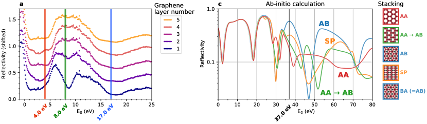
In Figure 1a, LEEM spectra are shown, taken on several locations of a TBG sample.
These LEEM spectra are directly related to layer count, as described in refs. [23, 24, 25, 22]; on the one hand via interlayer resonances in the 0–5 eV range, on the other hand via the gradual disappearance of a minimum at 8 eV.
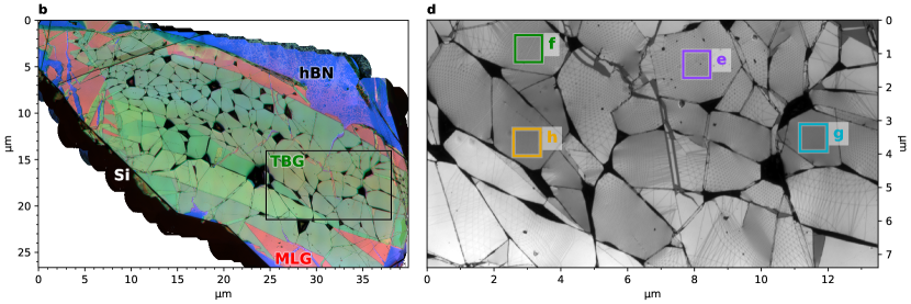
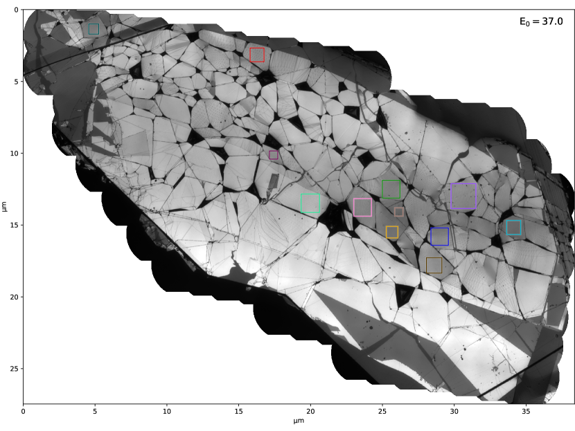
Here, more graphene layers (having a band gap at 8 eV) are progressively masking an hBN band underneath. This allows us to determine the local graphene layer count for each point on our sample. To visualize that, we choose three characteristic energies, i.e. (red), (green) and (blue) (see Figure 1a), and combine stitched overviews at these energies into a single false-color image (Figure 1b). This overview confirms that the sample consists of large TBG areas (darker green in Figure 1b) surrounded by monolayer graphene (pink), on an hBN flake (blue/purple) on silicon (black).
Stripes of brighter green indicate areas of 2-on-2 graphene layers (lower stripe), 2-on-1 (upper stripe), and 1-on-2 (wedge on the lower right). The relatively homogeneous areas are themselves separated by folds, appearing as black lines. The folds locally combine in larger dark nodes (confirmed by AFM, see Supplementary Information A).
A few folds, however, have folded over and appear as lines of higher layer count. Hence, Figure 1b provides a remarkable overview of a larger-scale sample, with detailed local information.
Increasing beyond , stacking boundaries and AA-sites become visible [23, 26].
This is consistent with ab-initio calculations of LEEM spectra for different relative stackings, as presented in Figure 1c.
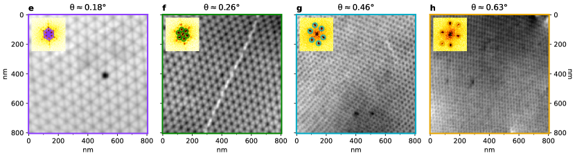
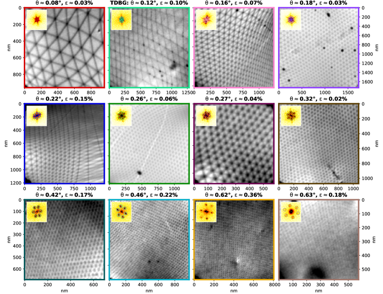
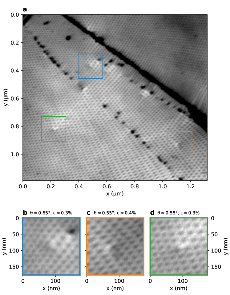
Therefore, imaging at (indicated in Figure 1c) yields a precise map of the moiré lattice over the full TBG area (see Figure 1d). We find that separate areas, between folds, exhibit different moiré periodicities and distortion [27].
This allows us to study different moiré structures on a single sample. Figure 1e-h shows full resolution crops of areas indicated in Figure 1d. The observed twist angles on this sample range from to 0.7∘.
For smaller angles, we observe local reconstruction towards Bernal stacking within the moiré lattice, consistent with literature [17, 20].
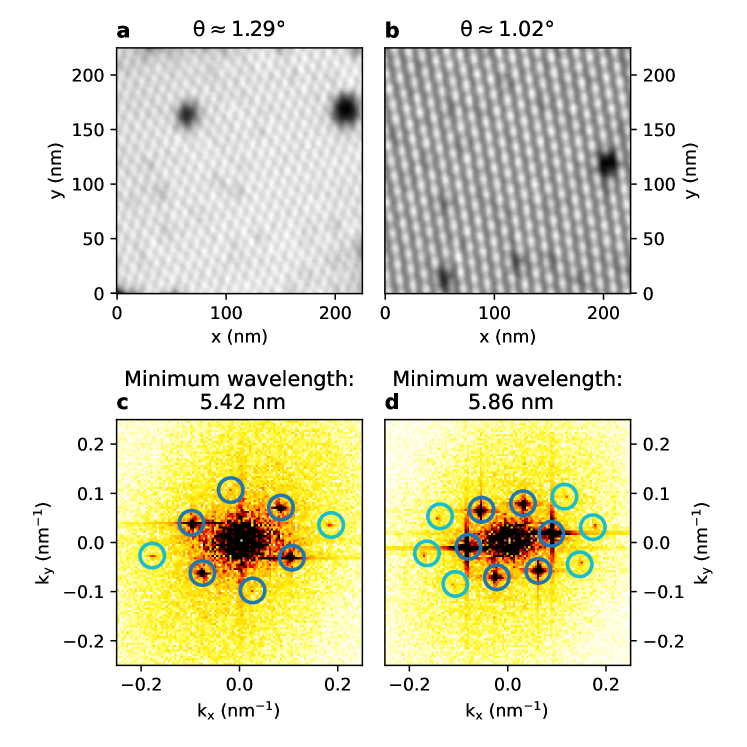
The best resolution was reached on another sample with a twist angle of 1.3∘ (See Supplementary Figure 11).
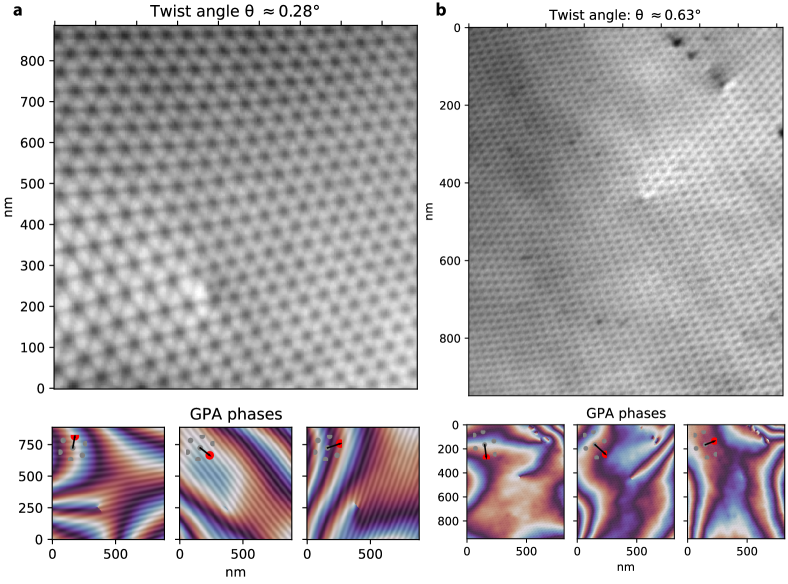
2.1 Distortions & Strain
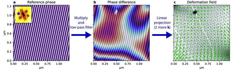
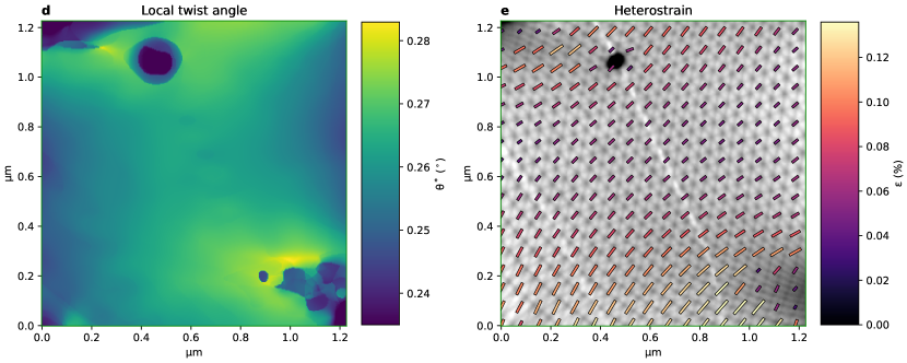
The moiré patterns shows distortions, corresponding to local variations in twist angle and (interlayer) strain. Near folds, for instance, the strain increases resulting in strongly elongated triangles, for example in the lower right corner of Figure 1d [28]. Despite their relative homogeneity, the moiré areas in Figure 1e-h also show subtle distortions. As structural variations correlate directly with local electronic properties, we quantify them in detail [5, 6]. For this, we use adaptive geometric phase analysis (GPA), extending our earlier work on STM data of moiré patterns in TBG (see Supplementary Information) [29, 30, 31, 32, 33]. This method, illustrated in Figure 2a-c, yields the displacement field with respect to a perfect lattice, by multiplying the original image with complex reference waves followed by low-pass filtering to obtain the GPA phase differences, which are then converted to the displacement field. This field fully describes the distortion of the moiré lattice and allows us to extract key parameters such as the local twist angle (see Figure 2d), and heterostrain magnitude and direction (see Figure 2e). [34, 31] The distortions of the moiré pattern correspond directly to distortions of the atomic lattices, magnified by a factor and rotated by [35, 31].
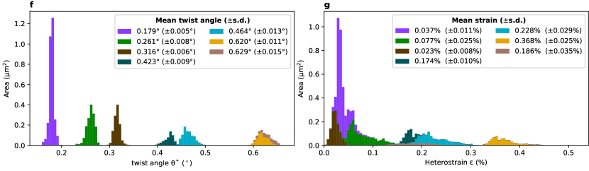
The extracted variation in twist angle and heterostrain for various regions of the sample, including those in Figure 1e-h, is summarized in Figure 2f,g, respectively. The twist angle variation within each domain is much smaller than the variation in twist angle between the separate, fold-bounded areas. Within domains, standard deviations range from 0.005∘ to 0.015∘, i.e. significantly smaller (by a factor 3–10) than previously reported [18, 31, 20]. The strain observed is around a few tenths of a percent, which is considerable. In some domains, we find an average strain of the atomic lattice of up to . According to earlier theoretical work, such values are high enough to locally induce a quantum phase transition [8].
The variation of , as for , within the domains is significantly lower than in earlier studies. We do note that the use of GPA introduces a point spread function (PSF) that is broader than the PSF of the instrument, resulting in a lower displacement field frequency response at small scales and therefore a somewhat reduced variation. Nevertheless, the combined PSF of instrument and analysis is still comparable to other techniques that do not image the unit cell directly, allowing for a direct comparison.
We hypothesize that the difference in variations with literature stems from the relatively high temperature at which we annealed and measured the sample, combined with the relatively long averaging time of this measurement (s for all data in Figure 2). The high temperature induces thermal fluctuations of the lattice (as demonstrated below), allowing the system to approach a lower energy, more homogeneous, state.
2.2 Edge dislocations
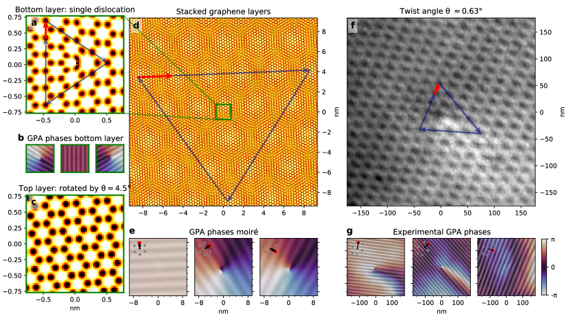
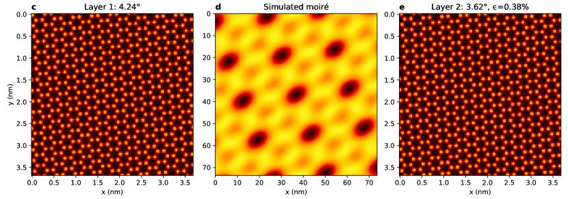
So far, we have discussed structural properties varying on the moiré length scale. However, the moiré magnification of deformations is general and extends to atomic edge dislocations (visualized in Figure 3a). This type of topological defect stems from a missing row of atomic unit cells and is characterized by an in-plane Burgers vector (in red) [36, 37]. The addition of a second (twisted) atomic layer magnifies (and rotates) the defect to an edge dislocation in the moiré lattice (illustrated in Figure 3d,e) [35]. In all cases, the defect can be characterized using GPA, pinpointing its location and Burgers vector (Figure 3b,e) [38].
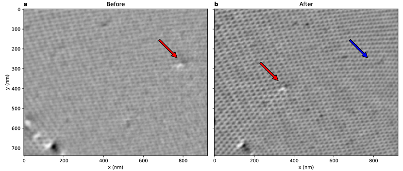
In our sample, we find a few such defects in the moiré lattice (see SI). In Figure 3f,g we show an edge dislocation in a topographically flat region with (see SI). Contrary to TEM observations on single-layer graphene [38], we do not observe creation or annihilation of edge dislocation pairs in the microscope, even at elevated measurement temperatures (500 ∘C) and under low-energy electron irradiation. Furthermore, the mobility of the defects is low. One edge dislocation did move, over several moiré cells between measurements, after which it remained at the same position even after a month at room temperature and reheating (see supplementary information). This stability suggests that the moiré lattice itself plays a role in stabilizing these defects, via a minimum of the local stacking fault energy within the moiré unit cell.
2.3 High temperature dynamics of the moiré lattice
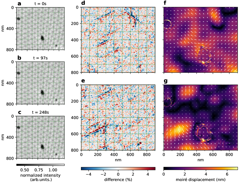
All measurements presented so far were performed at 500 ∘C, to minimize hydrocarbon contamination under the electron beam. In literature, there is concern about the graphene layers untwisting at such temperatures, due to energy differences between different rotations [14, 15]. We, however, see no sign of that. The twist angles within the domains are stable from 100 ∘C up to 600 ∘C for all samples studied. However, we did observe a more subtle thermal influence on the moiré pattern. At a temperature of 500 ∘C, the position of the stacking domain boundaries fluctuates slightly as a function of time (see Figure 4a-c). Taking the difference of later images (Figure 4b-c) with the first image (Figure 4a), we clearly see the domain boundaries shifting (Figure 4d,e). Moreover, we can quantify these fluctuations via the difference in displacement field with respect to the image at using GPA (Figure 4f,g). Interestingly, these involve the collective movement of millions of atoms, but only over very small distances.
We stress that a translation of the domain boundary by nm, as observed, corresponds to a shift of less than half the width of the domain boundary itself [17, 42]. As the relative shift of the layers over the full domain boundary is a single carbon bond length, the corresponding atomic translations are less than half of that, i.e. less than pm. Hence, the ‘moiré magnification’ makes it possible to detect these sub-Angstrom changes in TBG in real time using LEEM. Our data suggest that domain boundary displacement follows a random pattern of forward and backward steps. This indicates a possible source for the twist angle disorder observed in low(er) temperature experiments [20, 18, 31, 10]: frozen-in thermal fluctuations of the moiré lattice. The thermal fluctuations found, corresponding to for twist angle and for strain, are smaller than the extracted static deformations, though not negligible. Note that these values are damped by the intrinsic broadening of GPA and the time integration. Future experiments will focus on deducing the detailed statistics of the domain boundary dynamics versus temperature. Following these local collective excitations in time, will yield quantitative information on the energy landscape of these atomic lattice deformations within the moiré lattice. This will be important to answer the question if moiré lattices can be relaxed and homogenized using controlled annealing. If so, this would yield higher-quality magic-angle TBG devices in which charge transport is not limited by percolative effects and higher critical temperatures are reached.
3 Conclusion
Our quantitative LEEM study on TBG reveals a wide variety in twist angles and strain levels in a single sample. We show that spontaneous changes in global twist angle do not occur, even during high-temperature annealing, but that local collective fluctuations do take place. This suggests that high-temperature annealing causes relaxation of the local moiré lattice, reducing lattice disorder. Vice versa, this points to frozen-in thermal fluctuations as a possible source of the (significant) short-range twist angle disorder observed previously. Furthermore, this potentially offers insight into energetic aspects of the atomic lattice deformation within the moiré lattice.
We also report the observation of stable topological defects, i.e. edge dislocations, in the moiré lattice of two Van der Waals layers. Combining our methods with other techniques that can access the electronic structure, such as STS, nanoARPES, and even in-situ potentiometry [43], will allow for a systematic study of the electronic properties around these defects. Finally, the methods we describe here extend beyond TBG, to any type of twisted system. Therefore, our work introduces a new way of studying deformations of moiré patterns and of connecting these to the (local) electronic properties of this exciting class of materials.
4 Methods
4.1 Sample fabrication
The twisted bilayer graphene sample was fabricated using the standard tear-and-stack method [44, 1]. The monolayer graphene was first exfoliated with scotch tape on to a SiO2/Si substrate. A polycarbonate (PC)/polydimethylsiloxane (PDMS) stamp was used for the transfer process, where the PC covered only half of the PDMS surface. After the first half of the graphene flake was successfully torn and picked up, it was rotated by 1.0∘. The flake was then overlapped with the bottom half and used to pick it up. The stack was then stamped on a moderately thick (140nm) hBN flake, priorly exfoliated with PDMS on to a silicon substrate, along with the PC layer. Part of the graphene flake is deliberately put in contact with the Silicon surface for electrical contact purposes, i.e. to absorb the beam current. The whole substrate is then left in chloroform for 3 hours to dissolve the PC. All flakes were exfoliated from crystals, commercially bought from HQ Graphene and the fabrication process was performed using the Manual 2D Heterostructure Transfer System sold by the same company.
4.2 LEEM
All LEEM measurements where performed in the ESCHER LEEM, based on the SPECS P90 [11, 12, 45]. Samples were loaded into the ultrahigh-vacuum (base pressure better than ) LEEM main chamber and slowly heated to 500∘C (as measured by pyrometer and confirmed by IR-camera) and left to anneal overnight to get rid of any (polymer) residue. All measurements were conducted at elevated temperatures, 450∘C – 500∘C, unless specified otherwise. The sample was located on the substrate using photo-emission electron microscopy (PEEM) with an unfiltered mercury short-arc lamp, by comparing to optical microscopy images taken beforehand. Spectra were taken in high-dynamic-range mode and drift corrected and all images were corrected for detector artefacts, as described in ref. [46]. When needed to obtain a sufficient signal-to-noise ratio, multiple ms exposures were accumulated for each image, e.g. 8 exposures (2 seconds) per landing energy in the spectra in Figure 1b and 16 exposures (4 seconds) at each location for the overview at 37 eV in Figure 1c,e.
4.2.1 Time series
To measure the dynamics as presented in Figure 4, a time series of accumulated exposure images was taken back-to-back. After regular detector correction and drift correction, each image was divided by a Gaussian smoothed version of itself () to get rid of spatial and temporal fluctuations in electron illumination intensity. To further reduce noise, a Gaussian filter with a width of , was applied in the time direction before applying GPA.
4.3 Stitching
To enable high resolution, large field-of-view LEEM imaging, the LEEM sample stage [47] was scanned in a rectangular pattern over the sample, taking an image at each position, leaving sufficient overlap (m steps at a m field-of-view). To obtain meaningful deformation information from this, care needs to be taken to use a stitching algorithm that does not introduce additional deformation, i.e. as faithfully reproducing reality as the constituting images.
To achieve this, a custom stitching algorithm tailored towards such LEEM data, was developed, as described in the Supplementary information and in the implementation [48].
In addition, for the composite bright field in Figure 1a, minor rotation and magnifications differences due to objective lens focus differences were compensated for. This was done by registering the stitches for different energies using a log-polar transformation based method to obtain relative rotations and magnification. Subsequently, areas where a color channel was missing, were imputed using a -nearest neighbor lookup in a regularly sliced subset of the area with all color channels present.
4.4 Image analysis
To quantify the large deviations in lattice shape due to the moiré magnification of small lattice distortions, we extended the GPA algorithm to use an adaptive grid of reference wave vectors, based on related to earlier work in laser fringe analysis [32].
The spatial lock-in signal is calculated for a grid of wave vectors around a base reference vector, converting the GPA phase to reference the base reference vector every time. For each pixel, the spatial lock-in signal with the highest amplitude is selected as the final signal. To avoid the problem of globally consistent phase unwrapping, the gradient of each GPA phase was directly converted to the displacement gradient tensor. More details of the used algorithm are given in the Supplementary information.
All image analysis code was written in Python, using Numpy [49], Scipy [50], scikit-image [51] and Dask [52]. The core algorithms will be made available as an open source Python package [33]. Throughout the development of the algorithms and writing of the paper, matplotlib [53, 54] was extensively used for plotting and figure creation.
4.5 Reflectivity calculations
The theoretical reflectivity spectra are obtained with the ab-initio Bloch-wave-based scattering method described in ref. [55]. Details of the application of this method to stand-alone two-dimensional films of finite thickness can be found in ref. [56]. The underlying all-electron Kohn-Sham potential was obtained with a full-potential linear augmented plane-wave method within the local density approximation, as explained in ref. [57]. Inelastic scattering is taken into account by an absorbing imaginary potential , which is taken to be spatially constant () over a finite slab (where the electron density is non-negligible) and to be zero in the two semi-infinite vacuum half spaces. In addition, a Gaussian broadening of 1 eV is applied to account for experimental losses.
5 Acknowledgements
We thank Marcel Hesselberth and Douwe Scholma for their indispensable technical support. We thank D. K. Efetov and J. Aarts for getting us started on twisted bilayer graphene. We would like to thank J. Jobst and D.N.L. Kok for scientific discussions and L. Visser and G. Stam in particular for their input on the stitching algorithm. We thank Federica Galli for both scientific discussion as well as technical support. This work was supported by the Dutch Research Council (NWO) as part of the Frontiers of Nanoscience programme. It was also supported by the Spanish Ministry of Science, Innovation and Universities (Project No. PID2019-105488GB-I00).
6 Author contributions
TAdJ performed the LEEM measurements and wrote the LEEM data analysis code. XC fabricated the sample and performed AFM measurements. TB contributed to the analysis. EK performed the reflectivity calculations. TAdJ and SJvdM took the initiative for the writing of the manuscript, with contributions from several others. All authors contributed to the scientific discussion.
References
- [1] Yuan Cao et al. “Unconventional superconductivity in magic-angle graphene superlattices” In Nature 556.7699 Springer ScienceBusiness Media LLC, 2018, pp. 43–50 DOI: 10.1038/nature26160
- [2] R. Bistritzer and A.. MacDonald “Moire bands in twisted double-layer graphene” In Proceedings of the National Academy of Sciences 108.30 Proceedings of the National Academy of Sciences, 2011, pp. 12233–12237 DOI: 10.1073/pnas.1108174108
- [3] Xiaobo Lu et al. “Superconductors, orbital magnets and correlated states in magic-angle bilayer graphene” In Nature 574.7780 Springer ScienceBusiness Media LLC, 2019, pp. 653–657 DOI: 10.1038/s41586-019-1695-0
- [4] Simone Lisi et al. “Observation of flat bands in twisted bilayer graphene” In Nature Physics 17.2 Springer ScienceBusiness Media LLC, 2020, pp. 189–193 DOI: 10.1038/s41567-020-01041-x
- [5] Jia-Bin Qiao, Long-Jing Yin and Lin He “Twisted graphene bilayer around the first magic angle engineered by heterostrain” Publisher: American Physical Society In Physical Review B 98.23, 2018, pp. 235402 DOI: 10.1103/PhysRevB.98.235402
- [6] Zahra Khatibi, Afshin Namiranian and Fariborz Parhizgar “Strain impacts on commensurate bilayer graphene superlattices: Distorted trigonal warping, emergence of bandgap and direct-indirect bandgap transition” In Diamond and Related Materials 92, 2019, pp. 228–234 DOI: 10.1016/j.diamond.2018.12.007
- [7] Zhen Bi, Noah F.. Yuan and Liang Fu “Designing flat bands by strain” Publisher: American Physical Society In Physical Review B 100.3, 2019, pp. 035448 DOI: 10.1103/PhysRevB.100.035448
- [8] Daniel E. Parker et al. “Strain-Induced Quantum Phase Transitions in Magic-Angle Graphene” In Physical Review Letters 127.2 American Physical Society (APS), 2021 DOI: 10.1103/physrevlett.127.027601
- [9] Nikhil Tilak et al. “Flat band carrier confinement in magic-angle twisted bilayer graphene” In Nature Communications 12.1 Springer ScienceBusiness Media LLC, 2021 DOI: 10.1038/s41467-021-24480-3
- [10] Eva Y. Andrei and Allan H. MacDonald “Graphene bilayers with a twist” In Nature Materials 19.12 Springer ScienceBusiness Media LLC, 2020, pp. 1265–1275 DOI: 10.1038/s41563-020-00840-0
- [11] R.M. Tromp et al. “A new aberration-corrected, energy-filtered LEEM/PEEM instrument. I. Principles and design” In Ultramicroscopy 110.7 Elsevier BV, 2010, pp. 852–861 DOI: 10.1016/j.ultramic.2010.03.005
- [12] R.M. Tromp et al. “A new aberration-corrected, energy-filtered LEEM/PEEM instrument II. Operation and results” In Ultramicroscopy 127 Elsevier BV, 2013, pp. 25–39 DOI: 10.1016/j.ultramic.2012.07.016
- [13] Mikito Koshino and Young-Woo Son “Moiré phonons in twisted bilayer graphene” In Physical Review B 100.7 American Physical Society (APS), 2019 DOI: 10.1103/physrevb.100.075416
- [14] Youngjoon Choi et al. “Electronic correlations in twisted bilayer graphene near the magic angle” In Nature Physics 15.11 Springer ScienceBusiness Media LLC, 2019, pp. 1174–1180 DOI: 10.1038/s41567-019-0606-5
- [15] Yuan Cao et al. “Correlated insulator behaviour at half-filling in magic-angle graphene superlattices” In Nature 556.7699 Springer ScienceBusiness Media LLC, 2018, pp. 80–84 DOI: 10.1038/nature26154
- [16] Yonglong Xie et al. “Spectroscopic signatures of many-body correlations in magic-angle twisted bilayer graphene” In Nature 572.7767 Springer ScienceBusiness Media LLC, 2019, pp. 101–105 DOI: 10.1038/s41586-019-1422-x
- [17] Hyobin Yoo et al. “Atomic and electronic reconstruction at the van der Waals interface in twisted bilayer graphene” In Nature Materials 18.5 Springer ScienceBusiness Media LLC, 2019, pp. 448–453 DOI: 10.1038/s41563-019-0346-z
- [18] A. Uri et al. “Mapping the twist-angle disorder and Landau levels in magic-angle graphene” In Nature 581.7806 Springer ScienceBusiness Media LLC, 2020, pp. 47–52 DOI: 10.1038/s41586-020-2255-3
- [19] Dorri Halbertal et al. “Moiré metrology of energy landscapes in van der Waals heterostructures” In Nature Communications 12.1 Springer ScienceBusiness Media LLC, 2021 DOI: 10.1038/s41467-020-20428-1
- [20] Nathanael P. Kazmierczak et al. “Strain fields in twisted bilayer graphene” Publisher: Nature Publishing Group In Nature Materials, 2021, pp. 1–8 DOI: 10.1038/s41563-021-00973-w
- [21] Jan Ingo Flege and Eugene E. Krasovskii “Intensity-voltage low-energy electron microscopy for functional materials characterization” In physica status solidi (RRL) - Rapid Research Letters 8.6 Wiley, 2014, pp. 463–477 DOI: 10.1002/pssr.201409102
- [22] Johannes Jobst et al. “Quantifying electronic band interactions in van der Waals materials using angle-resolved reflected-electron spectroscopy” In Nature Communications 7.1 Springer ScienceBusiness Media LLC, 2016 DOI: 10.1038/ncomms13621
- [23] H Hibino, S Tanabe, S Mizuno and H Kageshima “Growth and electronic transport properties of epitaxial graphene on SiC” In Journal of Physics D: Applied Physics 45.15 IOP Publishing, 2012, pp. 154008 DOI: 10.1088/0022-3727/45/15/154008
- [24] R.. Feenstra et al. “Low-energy electron reflectivity from graphene” Publisher: American Physical Society In Physical Review B 87.4, 2013, pp. 041406 DOI: 10.1103/PhysRevB.87.041406
- [25] Tobias A. Jong et al. “Measuring the Local Twist Angle and Layer Arrangement in Van der Waals Heterostructures” In physica status solidi (b) 255.12 Wiley, 2018, pp. 1800191 DOI: 10.1002/pssb.201800191
- [26] T.. Jong et al. “Intrinsic stacking domains in graphene on silicon carbide: A pathway for intercalation” In Physical Review Materials 2.10 American Physical Society (APS), 2018 DOI: 10.1103/physrevmaterials.2.104005
- [27] Thomas E. Beechem, Taisuke Ohta, Bogdan Diaconescu and Jeremy T. Robinson “Rotational Disorder in Twisted Bilayer Graphene” In ACS Nano 8.2 American Chemical Society (ACS), 2014, pp. 1655–1663 DOI: 10.1021/nn405999z
- [28] Jinhai Mao et al. “Evidence of flat bands and correlated states in buckled graphene superlattices” Number: 7820 Publisher: Nature Publishing Group In Nature 584.7820, 2020, pp. 215–220 DOI: 10.1038/s41586-020-2567-3
- [29] M.J. Hÿtch, E. Snoeck and R. Kilaas “Quantitative measurement of displacement and strain fields from HREM micrographs” In Ultramicroscopy 74.3 Elsevier BV, 1998, pp. 131–146 DOI: 10.1016/s0304-3991(98)00035-7
- [30] M.. Lawler et al. “Intra-unit-cell electronic nematicity of the high-Tc copper-oxide pseudogap states” In Nature 466.7304 Springer ScienceBusiness Media LLC, 2010, pp. 347–351 DOI: 10.1038/nature09169
- [31] Tjerk Benschop et al. “Measuring local moiré lattice heterogeneity of twisted bilayer graphene” In Physical Review Research 3.1 American Physical Society (APS), 2021 DOI: 10.1103/physrevresearch.3.013153
- [32] Qian Kemao “Two-dimensional windowed Fourier transform for fringe pattern analysis: Principles, applications and implementations” In Optics and Lasers in Engineering 45.2 Elsevier BV, 2007, pp. 304–317 DOI: 10.1016/j.optlaseng.2005.10.012
- [33] Tobias A. Jong “pyGPA”, 2021 URL: https://github.com/TAdeJong/pyGPA
- [34] Alexander Kerelsky et al. “Maximized electron interactions at the magic angle in twisted bilayer graphene” In Nature 572.7767 Springer ScienceBusiness Media LLC, 2019, pp. 95–100 DOI: 10.1038/s41586-019-1431-9
- [35] Diana A. Cosma, John R. Wallbank, Vadim Cheianov and Vladimir I. Fal’ko “Moiré pattern as a magnifying glass for strain and dislocations in van der Waals heterostructures” Publisher: The Royal Society of Chemistry In Faraday Discussions 173.0, 2014, pp. 137–143 DOI: 10.1039/C4FD00146J
- [36] JM Burgers “Geometrical considerations concerning the structural irregularities to be assumed in a crystal” In Proceedings of the Physical Society (1926-1948) 52.1 IOP Publishing, 1940, pp. 23
- [37] R.W. Lardner “Mathematical Theory of Dislocations and Fracture” University of Toronto Press, 1971 DOI: 10.3138/9781487585877
- [38] J.. Warner et al. “Dislocation-Driven Deformations in Graphene” In Science 337.6091 American Association for the Advancement of Science (AAAS), 2012, pp. 209–212 DOI: 10.1126/science.1217529
- [39] A. Mesaros, D. Sadri and J. Zaanen “Berry phase of dislocations in graphene and valley conserving decoherence” In Physical Review B 79.15 American Physical Society (APS), 2009 DOI: 10.1103/physrevb.79.155111
- [40] Yi-Wen Liu, Ya-Ning Ren, Chen-Yue Hao and Lin He “Direct observation of magneto-electric Aharonov-Bohm effect in moir\’e-scale quantum paths of minimally twisted bilayer graphene” arXiv: 2102.00164 In arXiv:2102.00164 [cond-mat], 2021 URL: http://arxiv.org/abs/2102.00164
- [41] C. De Beule, F. Dominguez and P. Recher “Aharonov-Bohm Oscillations in Minimally Twisted Bilayer Graphene” Publisher: American Physical Society In Physical Review Letters 125.9, 2020, pp. 096402 DOI: 10.1103/PhysRevLett.125.096402
- [42] Fernando Gargiulo and Oleg V. Yazyev “Structural and electronic transformation in low-angle twisted bilayer graphene” Publisher: IOP Publishing In 2D Materials 5.1, 2017, pp. 015019 DOI: 10.1088/2053-1583/aa9640
- [43] J. Kautz et al. “Low-Energy Electron Potentiometry: Contactless Imaging of Charge Transport on the Nanoscale” Number: 1 Publisher: Nature Publishing Group In Scientific Reports 5.1, 2015, pp. 13604 DOI: 10.1038/srep13604
- [44] Kyounghwan Kim et al. “Tunable moiré bands and strong correlations in small-twist-angle bilayer graphene” In Proceedings of the National Academy of Sciences 114.13 Proceedings of the National Academy of Sciences, 2017, pp. 3364–3369 DOI: 10.1073/pnas.1620140114
- [45] S.. Schramm et al. “Low-energy electron microscopy and spectroscopy with ESCHER: Status and prospects” In IBM Journal of Research and Development 55.4 IBM, 2011, pp. 1:1–1:7 DOI: 10.1147/jrd.2011.2150691
- [46] T.A. Jong et al. “Quantitative analysis of spectroscopic Low Energy Electron Microscopy data: High-dynamic range imaging, drift correction and cluster analysis” In Ultramicroscopy Elsevier BV, 2019, pp. 112913 DOI: 10.1016/j.ultramic.2019.112913
- [47] A.. Ellis and R.. Tromp “A versatile ultra high vacuum sample stage with six degrees of freedom” In Review of Scientific Instruments 84.7 AIP Publishing, 2013, pp. 075112 DOI: 10.1063/1.4813739
- [48] Tobias A. Jong “TAdeJong/LEEM-analysis: LEEM-analysis” Zenodo, 2019 DOI: 10.5281/ZENODO.3539538
- [49] Charles R. Harris et al. “Array programming with NumPy” In Nature 585.7825 Springer ScienceBusiness Media LLC, 2020, pp. 357–362 DOI: 10.1038/s41586-020-2649-2
- [50] Pauli Virtanen et al. “SciPy 1.0: Fundamental Algorithms for Scientific Computing in Python” In Nature Methods 17, 2020, pp. 261–272 DOI: 10.1038/s41592-019-0686-2
- [51] Stéfan Walt et al. “scikit-image: image processing in Python” In PeerJ 2 PeerJ, 2014, pp. e453 DOI: 10.7717/peerj.453
- [52] Dask Development Team “Dask: Library for dynamic task scheduling”, 2016 URL: https://dask.org
- [53] J.. Hunter “Matplotlib: A 2D graphics environment” In Computing in Science & Engineering 9.3 IEEE COMPUTER SOC, 2007, pp. 90–95 DOI: 10.1109/MCSE.2007.55
- [54] Thomas A Caswell et al. “matplotlib/matplotlib: REL: v3.3.2” Zenodo, 2020 DOI: 10.5281/ZENODO.4030140
- [55] E.. Krasovskii “Augmented-plane-wave approach to scattering of Bloch electrons by an interface” In Physical Review B 70, 2004, pp. 245322 DOI: 10.1103/PhysRevB.70.245322
- [56] Eugene Krasovskii “Ab Initio Theory of Photoemission from Graphene” In Nanomaterials 11.5, 2021 DOI: 10.3390/nano11051212
- [57] E.. Krasovskii, F. Starrost and W. Schattke “Augmented Fourier components method for constructing the crystal potential in self-consistent band-structure calculations” In Physical Review B 59, 1999, pp. 10504 DOI: 10.1103/PhysRevB.59.10504
- [58] Siu Kwan Lam, Antoine Pitrou and Stanley Seibert “Numba” In Proceedings of the Second Workshop on the LLVM Compiler Infrastructure in HPC - LLVM ’15 ACM Press, 2015 DOI: 10.1145/2833157.2833162
Supplementary information
Appendix A AFM comparison
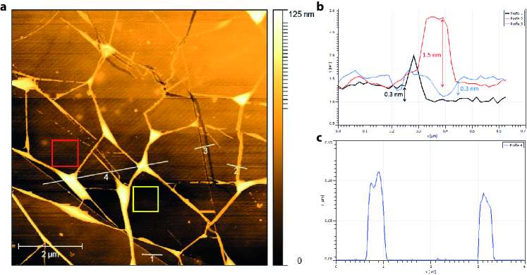
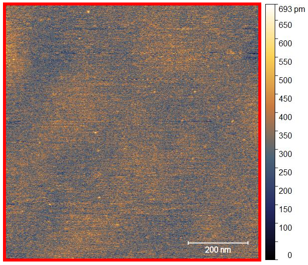
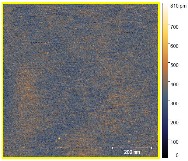
To further characterize the surface properties of the sample, an AFM (JPK, NanoWizard 3) measurement was performed in AC tapping mode following the LEEM measurements. Predominantly, the results show a very flat and clean graphene surface between folds, indicating annealing at 500 ∘C in UHV had successfully removed the polymer residue left on the surface.
In profile 1, the terrace height sees a difference of 0.3 nm, demonstrating the graphene layer count goes down by one at this location. This corresponds to the layer counts extracted from the LEEM spectra.
Profile 2 to 4 shows 3 different kinds of defects in the bilayer graphene region. The ridge at location 2 seems to be a neat folding of both the bilayer graphene flake (1.5 nm in height, four layers of graphene), whereas profile 4 shows wrinkles that are up to 120 nm tall. This is also reflected by the distinct patterns in the LEEM bright field overview image, respectively. While the wrinkles merely appear black, the ridge resembles more like a unique layer count domain. Profile 3 shows two tears within the one layer of graphene, corresponding nicely to the defect region observed in LEEM where monolayer graphene shines through.
The zoomed-in small scale measurements marked by the red and yellow box shows the topography on top of two dislocations observed in LEEM. As shown in Figure 6, no distinctive feature was observed at either dislocation. The topography, however, shows an exceptionally flat surface with a height variation (peak-to-peak) of less than 1 nm.
Appendix B Supplementary notes on Adaptive GPA
Regular GPA is limited in the wave vector deviations (with respect to the reference wave vector) it can measure, due to the limitations in spectral leakage. This is no problem when applied to atomic lattices, as the expected deviations are very small there. However, due to the moiré magnification of small lattice distortions, it does become a limiting factor when applying GPA to small twist angle moiré lattices.
To overcome this limitation, we extended the GPA algorithm to use adaptive reference wave vectors, based on the combination of two ideas and related to earlier work in laser fringe analysis [32]: First, a GPA phase calculated with respect to one reference vector can always be converted to the GPA phase with respect to another reference vector by adding a phase corresponding to the phase difference between the reference vectors. Second, a larger lock-in amplitude corresponds to a better fit between the reference vector and the data.
The adaptive GPA algorithm therefore works as follows: The spatial lock-in signal is calculated for a grid of wave vectors around a base reference vector, converting the GPA phase to reference the base reference vector every time. For each pixel, the spatial lock-in signal with the highest amplitude is selected as the final signal.
It was realized that to deduce the deformation properties, reconstruction to a globally consistent phase (requiring 2D phase unwrapping), as reported previously [31], is not strictly needed, making it possible to circumvent the problems associated with 2D phase unwrapping. Instead, the gradient of each GPA phase was calculated, requiring only local 1D phase unwrapping (i.e. assuming the derivative of the phase in both the and direction will never be more than per pixel, an assumption in practice always met). Subsequently, these three GPA gradients are converted to the displacement gradient tensor (in real space coordinates), estimating the transformation via weighted least squares, using the local spatial lock-in amplitudes as weights.
As an added benefit, this entire procedure is local, i.e. not depending on pixels beyond nearest neighbors in any way except for the initial Gaussian convolution in determining the GPA. This reduces the effect of artefacts in the image to a minimum local area around each artefact (where for in the 2D phase unwrapping they have a global influence on the phases).
However, when the gradient is computed based on phase values stemming from two different GPA reference vectors, i.e. at the edge of their valid/optimal regions, artefacts appear due to their relatively large absolute error. To prevent this, the local gradient of the phase with the highest lock-in magnitude is stored alongside the lock-in signal itself in the GPA algorithm. This way, the gradient is calculated based on a single reference phase, propagating only the much smaller relative/derivative error between the two signals instead of the absolute error.
As mentioned in the main text, even adaptive GPA has its limits. In particular, too large deviations from the base reference vector can not be resolved correctly, causing an erroneous, lower, extracted deviation, as is visible in the lower right of Figure 2e in the main text). As the deformation becomes too large, e.g. towards the folds in the TBG, the highest lock-in amplitude will occur at a different moiré peak or at the near-zero components of the fourier transform, causing an incorrect value to be extracted.
Appendix C Supplementary note on the decomposition of the displacement field.
Kerelsky et al. [34] use the following idea to extract twist angle , strain magnitude and strain direction from reciprocal moiré lattice vectors : These difference vectors of the constituting atomic lattices are written in terms of a rotated and a strained lattice vector each:
where are the original lattice vectors. Kerelsky et al. assume to be along the -axis, and get around this by taking amplitudes, discarding any global rotation. Here, we do however introduce that global rotation, by a multiplication with :
Eihter of these expressions can, and indeed by Kerelsky et al. is, numerically fitted to the found amplitudes or -vectors for each triangle. However, from GPA analysis we most naturally obtain a Jacobian transformation of the moiré -vectors with respect to some specific set of reference vectors with predefined strain and rotations:
Note that we can force .
This simplifies to:
| The linear transformation is uniquely described by its effect on two points in -space, so their matrix representations should be equal: | ||||
The left hand side is a known quantity at each position, the right hand side remains to be numerically fitted or extracted. This is implemented in pyGPA using scipy.optimize and numba to just-in-time compile the fitting code [33, 58].
Alternatively, we could formulate a symmetric expression with two strains, but without allowing for further joint rotation of the lattices:
Appendix D LEEM stitching
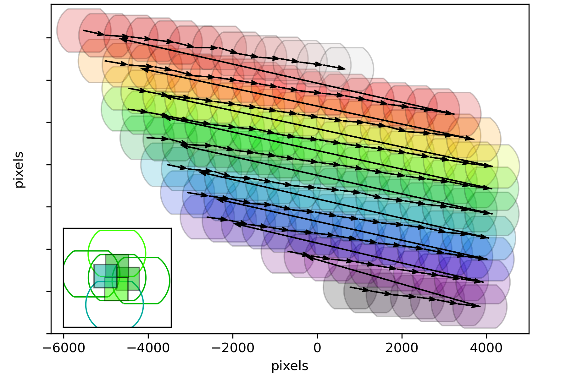
To achieve stitching of images without inducing any additional deformation, a custom stitching algorithm tailored towards such LEEM data, was developed, working as follows:
To compensate sample stage inaccuracy, nearest neighbor (by sample stage coordinates) images are compared, finding their relative positions by cross-correlation. Using an iterative procedure, calculating cross correlations of overlapping areas at each step, the absolute positions of all images are found. Images are then combined in a weighted fashion, with the weight sloping to zero at the edges of each image, to smooth out any mismatch due to residual image warping. The full stitching algorithm is implemented in Python, available as a Jupyter Notebook[48].
It is designed for use with ESCHER LEEM images. For those images, their positions are known approximately in terms of stage coordinates, i.e. the positions as reported by the sensors in the sample stage. It should however generalize to any set of overlapping images where relative positions of the images are known in some coordinate system which can approximately be transformed to coordinates in terms of pixels by an affine transformation (rotation, translation, mirroring).
The algorithm consists of the following steps:
-
1.
Using the stage coordinates for each image, obtain a nearest neighbour graph with the nearest n_neighbors neighbouring images for each image.
-
2.
Obtain an initial guess for the transformation matrix between stage coordinates and pixel coordinates, by one of the following options:
-
1.
Copying a known transformation matrix from an earlier run of a comparable dataset.
-
2.
Manually overlaying some nearest neighbor images from the center of the dataset, either refining the estimate, or making a new estimate for an unknown dataset
-
1.
-
3.
Calculate an initial estimate of the pixel coordinates of the images by applying the corresponding transformation to the stage coordinates
-
4.
Apply a gaussian filter with width sigma to the original dataset and apply a magnitude sobel filter. Optionally scale down the images by an integer factor z in both directions to be able to reduce fftsize by the same factor, without reducing the sample area compared.
-
5.
Iterate the following steps until the calculated image positions have converged to within sigma:
-
1.
Obtain a nearest neighbour graph with per image the nearest n_neighbors neighbouring images from the current estimate of the pixel coordinates and calculate the difference vectors between each pair of nearest neighbours.
-
2.
For each pair of neighboring images:
-
i.
Calculate the cross-correlation between areas estimated to be in the center of the overlap of size fftsize*fftsize of the filtered data. If the estimated area is outside the valid area of the image defined by mask/radius, take an area as close to the intended area but still within the valid area as possible.
-
ii.
Find the location of the maximum in the cross-correlation. This corresponds to the correction to the estimate of the difference vector between the corresponding image position pair.
-
iii.
Calculate the weight of the match by dividing the maximum in the cross-correlation by the square root of the maximum of the auto-correlations.
-
i.
-
3.
Compute a new estimate of the difference vectors by adding the found corrections. Reconvert to a new estimate of pixel coordinates by minimizing the squared error in the system of equations for the positions, weighing by modified weights, either:
-
i.
for , else, with the maximum lower bound such that the graph of nearest neighbours with non-zero weights is still connected
-
ii.
Only use the ‘maximum spanning tree’ of weights, i.e. minus the minimum spanning tree of minus the weights, such that only the best matches are used.
-
i.
-
1.
-
6.
(Optional) Refine the estimate of the transformation matrix, using all estimated difference vectors with a weight better than and restart from step 3.
-
7.
Repeat step 4. and 5. until sigma is satisfactory small. Optional repeat a final time with the original data if the signal to noise of the original data permits.
-
8.
Select only the images for stitching where the average of the used weights (i.e. where ) is larger than for an appropriate value of .
-
9.
(Optional) For those images, match the intensities by calculating the intensity ratios between the overlap areas of size fftsize*fftsize and perform a global optimization.
-
10.
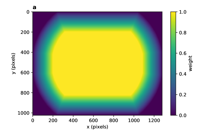
Define a weighting mask, 1 in the center and sloping linearly to zero at the edges of the valid region, over a width of bandwidth pixels, as illustrated in Figure 8.
-
11.
Per block of output blocksize*blocksize, select all images that have overlap with the particular output block, multiply each by the weighting mask and shift each image appropriately. Divide by an equivalently shifted stack of weighting masks. As such information at the center of images gets prioritized, and transitions get smoothed.
D.1 Considerations
For square grids with a decent amount of overlap, it makes sense to put n_neighbors to 5 (including the image itself), however, for larger overlaps or datasets where an extra dimension is available (such as landing energy), it can be appropriate to increase the number of nearest neighbors to which each image is matched.
Parameters and intermediate results of the iteration are saved in an xarray and saved to disk for reproducibility.
D.2 Parallelization
Using dask, the following steps are parallelized:
-
•
step 5B , where each pair of images can be treated independently. In practice parallelization is performed over blocks of subsequent images with their nearest neighbours. This could be improved upon in two ways: firstly by treating each pair only once, and secondly by making a nicer selection of blocks of images located close to each other in the nearest neighbor graph. This would most likely require another (smarter) data structure than the nearest neighbour indexing matrix used now.
-
•
Step 6 is quite analogous to 5B and is parallelized similarly.
-
•
Step 11 is parallelized on a per block basis. To optimize memory usage, results are directly streamed to a zarr array on disk.
-
•
The minimizations are parallelized by scipy natively.
Appendix E Additional images/crops
Appendix F Supplementary figures dislocations
Appendix G Dynamics
Full movie showing larger Field of View compared to Figure 4, in real space data, difference data and GPA-extracted displacement field.