Band tail formation in mono and multilayered transition metal dichalcogenides: A detailed assessment and a quick-reference guide
Abstract
Transition metal dichalcogenides (TMDs) are promising candidates for a wide variety of ultrascaled electronic, quantum computation, and optoelectronic applications. The exponential decay of electronic density of states into the bandgap, i.e. the band tail has a strong impact on the performance of TMD applications. In this work, the band tails of various TMD monolayer and multilayer systems when placed on various dielectric substrates is predicted with density functional theory based nonequilibrium Green’s functions. Nonlocal scattering of electrons on polar optical phonons, charged impurities and remote scattering on phonons in the dielectric materials is included in the self-consistent Born approximation. The band tails are found to critically depend on the layer thickness, temperature, doping concentration and particularly on the chosen dielectric substrate. The underlying physical mechanisms are studied in high detail and an analytical interpolation formula is given to provide a quick-reference for Urbach parameters in MoS2, WS2 and WSe2.
I Introduction
Two dimensional materials have attracted considerable attention due to their unique electronic, optical and mechanical properties Novoselov et al. (2005); Wang et al. (2012); Jariwala et al. (2014); Mak and Shan (2016); Manzeli et al. (2017). Transition metal dichalcogenides (TMDs) have a finite band gap making it an attractive alternative in electronics for Si/SiGe based transistors Desai et al. (2016); Podzorov et al. (2004); Liu et al. (2011); Huyghebaert et al. (2018), in optoelectronics as possible materials in light emitting diodes Cheng et al. (2014); Baugher et al. (2014); Zhou et al. (2018); Gu et al. (2019); Bie et al. (2017); Zheng et al. (2018) and solar cell applications Tsai et al. (2014); Dasgupta et al. (2017); Tsai et al. (2014); Yang et al. (2014). TMD layers are coupled by weak van der Waals forces only which allows for mechanical cleavage of bulk TMD materials into mono and multilayer systems. Those systems yield electronic and optical properties that depend strongly on the number of layers Wang et al. (2017). Stacking multiple TMD layers on top of each other significantly widens the available material design space Pospischil and Mueller (2016); Memaran et al. (2015) resulting in a plethora of ultra thin devices such as stacked optoelectronic p-n junctions Lee et al. (2014); Zhang et al. (2016a); Mak and Shan (2016), photovoltaics Yu and Sivula (2017); Wu et al. (2019); Das et al. (2019) as well as ultra scaled non-volatile and neuromorphic memory devices Park et al. (2020); Cao et al. (2020); Wang et al. (2019). Electrons in TMDs scatter on phonons, defects and charged impurities which leads to band tails (also known as Urbach tails), i.e. exponentially decaying density of states in the band gap Halperin and Lax (1966); Sarangapani et al. (2019) Schenk (1998); Sernelius (1986); Halperin and Lax (1966, 1967); Van Mieghem (1992). The slope of the exponential density of states tail is known as the Urbach parameter. Urbach tails can significantly alter the device performance: The switching of transistors is drastically affected by these tails Lu and Seabaugh (2014); Agarwal and Yablonovitch (2014); Bizindavyi et al. (2018). They affect the optical behaviour such as absorption spectra and absorption/recombination coefficients in optoelectronic devices Hebig et al. (2016); Ikhmayies and Ahmad-Bitar (2013); Guerra et al. (2016). They also set a fundamental limit on the subthreshold performance of semiconductor devices at cryogenic temperatures for large-scale quantum computing applications. Beckers et al. (2019, 2021) Since electron-phonon and electron-defect interaction cause the Urbach tails to form, the Urbach parameter is strongly dependent on temperature and doping concentration. Halperin and Lax (1966, 1967); John et al. (1986); Jain and Roulston (1991). State-of-the-art models for the Urbach parameter of specific materials are either heuristic or the parameters are directly extracted from experimental observations. Halperin and Lax (1966); Van Mieghem (1992); Halperin and Lax (1967); Jain and Roulston (1991); Zhang et al. (2016b); Bizindavyi et al. (2018); Schenk (1998); Sernelius (1986). TMD based nanodevices typically interface the TMD layers with various oxides. Therefore, TMD device electrons scatter on remote phonons as well Van de Put et al. ; Jena and Konar (2007). Experiments for several TMDs have shown that their Urbach tails depend on the oxide type Amani et al. (2015); Fang et al. (2014). Different scattering mechanisms can interfere with each other and impact the electronic density of states which is hard to estimate without detailed calculations. Jirauschek and Kubis (2014); Eliashberg (1960); Sarangapani et al. (2019). This is further complicated by the strong dependence of electronic and scattering properties in TMD systems on the number of atomic layers and their environment Kumar and Ahluwalia (2012); Jena and Konar (2007); Ma and Jena (2014). Therefore, this work predicts Urbach parameters for MoS2, WS2 and WSe2 layer systems as a function of layer thickness, temperature, doping concentration, and oxide type (comprising Al2O3, HfO2, SiO2 and h-BN) with DFT-based quantum transport calculations Szabó et al. (2015); Afzalian (2021) for electronic Green’s functions including scattering on various types of phonons, charged impurities and remote scattering on oxide phonons with NEMO5. Charles et al. (2016); Sarangapani et al. (2019); Lemus et al. (2020). We delineate the contribution of different scattering mechanisms towards the Urbach parameter and gain insight into its dependence on layer thickness and oxide type. All calculations in this work are based on the non-equilibrium Green’s function (NEGF) implementation of NEMO5. NEGF is well suited to analyze Urbach parameters Sarangapani et al. (2019); Khayer and Lake (2011) since it is a method of choice to predict electronic behavior when incoherent scattering and coherent quantum effects are equally important. Electronic, thermal and optoelectronic systems with nanoscale dimensions or pronounced nonequilibrium conditions are a few such examples Lake et al. (1997); Markussen et al. (2009); Lee and Wacker (2002); Kubis et al. (2009); Sarangapani et al. (2018); Chu et al. (2019); Geng et al. (2018); Wang et al. (2020).This work summarizes the quantum transport calculations with an easily accessible lookup formula to predict Urbach parameters of MoS2, WS2 and WSe2 layer systems as a function of layer thickness, temperature, doping concentration, and oxide type.
II Simulation Approach
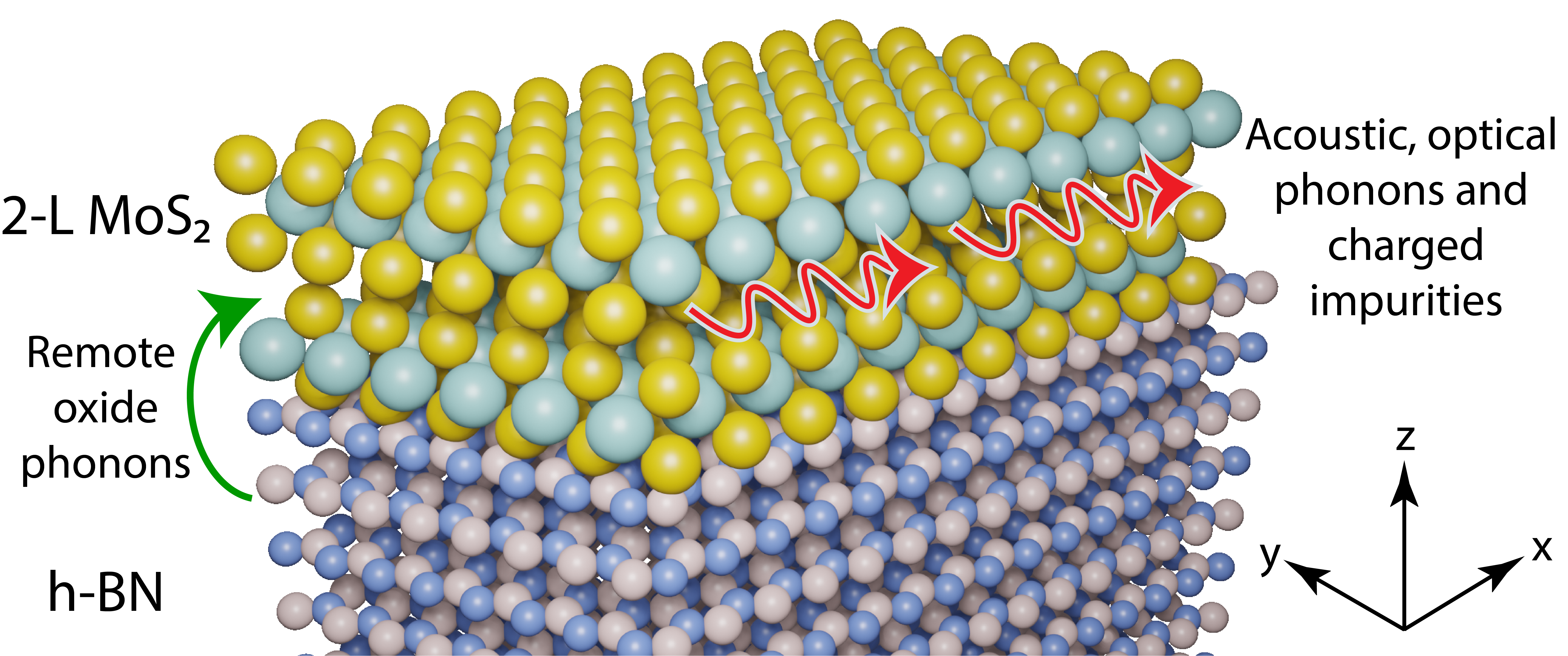
All TMD structures considered in this work are represented in their native atomic lattice. Electrons are sub-atomically resolved with maximally localized Wannier functions (MLWFs) derived from DFT Hamiltonians. Wang et al. (2017); Szabó et al. (2015). The process of generating electronic Hamiltonian operators requires first to perform a self-consistent electronic structure calculation with the DFT tool VASP Hafner (2008) with a convergence criterion of eV. A momentum mesh of Monkhorst-Pack grid and an energy cutoff of 520 eV is used along with van-der-Waals force included following Ref. Bucko et al., 2010. The applied DFT model is the generalized gradient approximation (GGA) employing the Perdew-Burke-Ernzerhof (PBE) functionals. The resulting DFT Hamiltonian is then transformed into an MLWF representation using the Wannier90 software Marzari and Vanderbilt (1997); Thygesen et al. (2005); Das et al. (2017) with d orbitals for the metal sites and sp3 hybridized orbitals for the chalcogenide sites as the initial projection. The spreading of the Wannier functions is reduced iteratively until it converges to around . The atom positions and their corresponding electronic Hamiltonian of finite TMD structures are then imported into NEMO5 for NEGF calculations. All electronic Green’s functions are solved in the self-consistent Born approximation with self-energies representing each incoherent scattering mechanism (scattering of electrons with acoustic phonons (AP), polar optical phonons (POP), charged impurities (CI) and remote phonons (RP) from the oxide. Since the structures are assumed to be periodic in the transverse Y direction (see Fig. 1), the electronic Green’s functions and self-energies depend on the electronic energy and and in-plane momentum . The corresponding Brillouin zone is resolved with 25 points. All Green’s functions and self-energies are matrices with respect to the MLWF orbitals along the directions. (see Fig. 1). Each scattering processes is modeled with a corresponding retarded and lesser scattering self-energy Lake et al. (1997); Jirauschek and Kubis (2014). The imaginary part of the retarded self-energy provides information about the scattering rate of the electrons Wacker (2002). The real part of the retarded self-energies yields an energy shift of electronic states Sarangapani et al. (2019); Esposito et al. (2009). Since this work focuses on the Urbach parameter only, the real part of all retarded scattering self-energies is ignored.
In this work, the Green’s functions of electrons are explicitly solved, whereas Green’s functions of phonons are approximated as plane waves occupied with the equilibrium Bose distribution . The 3 acoustic phonon types (LA, TA, ZA) are averaged into a single effective deformation potential and sound velocity. The corresponding self-energy given in Ref. Kubis et al., 2009 is multiplied by 3x accordingly. Polar optical phonons (POP) are modeled with a constant, material dependent phonon energy . Scattering on charged impurities (CI) is assumed to be elastic. POP and CI are based on long-range Coulomb interaction and therefore yield non-local scattering self-energies. Mahan (2013); Jacoboni (2010) To limit the numerical burden of solving self-energies and Green’s functions but still faithfully predict the POP and CI scattering, the respective self-energies are approximated to be local and multiplied with a material and device dependent compensation factor. The detailed expressions for POP and CI scattering self-energies and the compensation factor are given in Ref Sarangapani et al., 2019. The interaction potential of electrons and remote oxide phonons is taken from Ref. Fischetti et al., 2001. The resulting lesser and retarded scattering self-energies for electrons remotely scattering on the two surface optical oxide phonon modes () are given by
| (1) |
| (2) |
where
| (3) |
is the optical phonon frequency of the underlying oxide, and are the static and infinite frequency dielectric constants of the oxide, is the infinite frequency dielectric constant of the TMD. The oxide phonon modes are considered to exponentially decay into the TMD with and the distances of the two electron propagation coordinates from the oxide-semiconductor interface (see Fig. 1). is the thickness of the TMD system. is the Bessel-J function of 0’th order. The electrostatic screening of electron and holes is represented by and calculated with the Lindhard formula Lindhard (1954) (Add the 2D formula with more details)
| (4) |
where is the Fermi distribution function and the momentum integral runs over the first Brillouin zone.
For all the discussions in the subsequent sections, the electrons are solved in equilibrium. The electronic Fermi level is determined such that the spatially integrated electron density agrees with the integrated doping concentration to achieve global charge neutrality. The Green’s functions are solved with the Dyson and Keldysh equations:
| (5) |
All scattering self-energies are self-consistently solved with the Green’s functions until the relative particle current variation is less than 1e-5 throughout the device. The source and drain contact self-energies are solved following Ref. Sancho et al. (1985). Urbach parameter is extracted from the exponentially decaying spatially averaged density of states below (above) the conduction (valence) band. Sarangapani et al. (2019) Those Urbach parameters correspond to the ones measured in transport experiments. In contrast, optical measurements relate to excitons which require a different scattering model. All other material parameters for the TMDs and oxides are taken from Refs Kumar and Ahluwalia (2012); Jin et al. (2014); Ma and Jena (2014) and listed in Table 1 and 2.
| Material | Layer | (m/s) | (kg/m3) | (meV) | D (eV/nm) | POP scattering prefactor | ||
|---|---|---|---|---|---|---|---|---|
| 1 | 7200 | 5060 | 48 | 4.5 | 3.8 | 3.2 | 0.4069 | |
| 2 | 5.37 | 5.65 | 4.8 | 0.2584 | ||||
| 3 | 6.25 | 6.47 | 5.5 | 0.2248 | ||||
| 4 | 7.12 | 7.3 | 6.2 | 0.2004 | ||||
| 1 | 6670 | 7500 | 33 | 3.2 | 3.65 | 3.1 | 0.5847 | |
| 2 | 4.07 | 5.15 | 4.37 | 0.4169 | ||||
| 3 | 4.95 | 5.92 | 5.03 | 0.3595 | ||||
| 4 | 5.82 | 6.7 | 5.69 | 0.3187 | ||||
| 1 | 5550 | 9320 | 30 | 3.2 | 3.7 | 3.145 | 0.6167 | |
| 2 | 4.07 | 5.3 | 4.5 | 0.4337 | ||||
| 3 | 4.95 | 6.1 | 5.18 | 0.3765 | ||||
| 4 | 5.82 | 6.9 | 5.86 | 0.3326 |
| Oxide | (meV) | (meV) | ROP scattering prefactor | ||
|---|---|---|---|---|---|
| 93.07 | 179.10 | 5.09 | 4.10 | 0.1159 | |
| 55.60 | 138.10 | 3.90 | 2.50 | 1.0478 | |
| 48.18 | 71.41 | 12.53 | 3.20 | 2.9231 | |
| 12.40 | 48.35 | 23.00 | 5.03 | 3.6363 |
III Results
III.1 Band tails: Intrinsic to the material
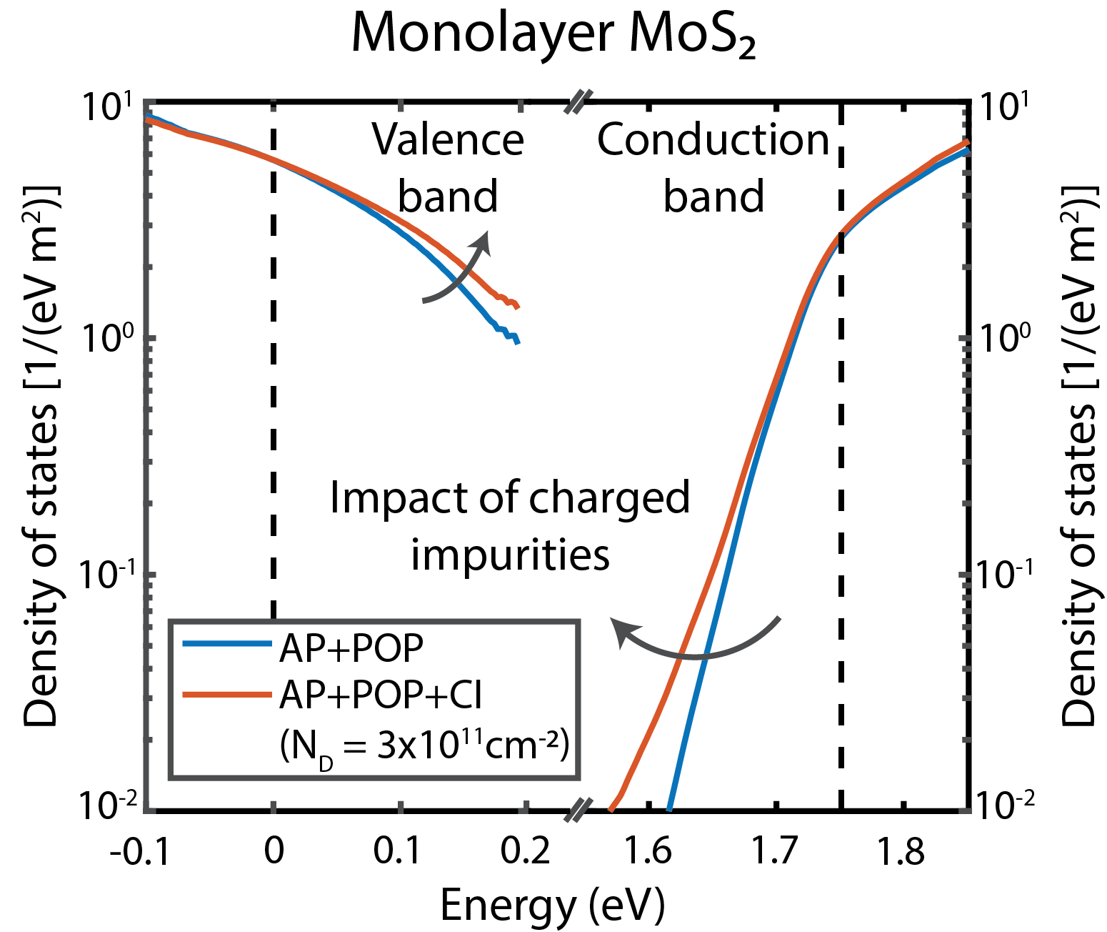
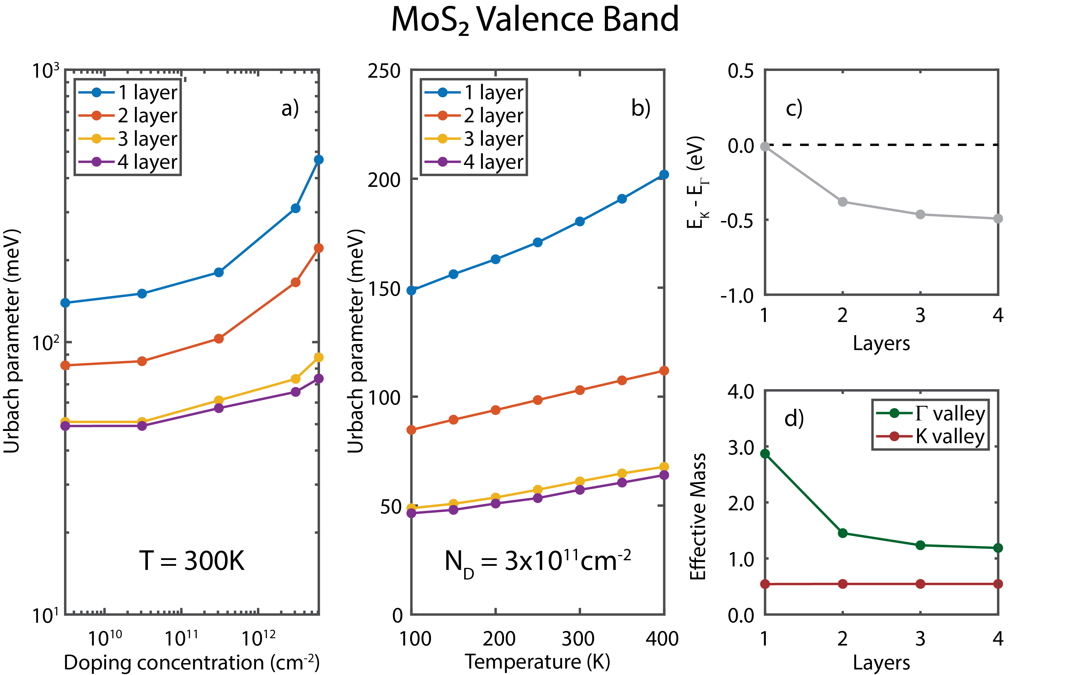
Electronic scattering on polar optical phonons (POP) creates finite density of states above (below) the valence (the conduction) band that decays exponentially into the band gap (see Fig. 2). The slope of this band tail, i.e. the Urbach parameter increases with incoherent scattering of electrons on charged impurities (as also observed in Ref. Sarangapani et al., 2019). The scattering rates are proportional to the imaginary retarded scattering self-energies ()Wacker (2002). In the self-consistent Born approximation is proportional to the retarded Green’s function () (see Eq. 1 and Refs. Sarangapani et al. (2019); Charles et al. (2016).). Therefore, the strength of the scattering processes that form Urbach tails is determined by the imaginary part of , i.e. the density of states at the band edges Sarangapani et al. (2019). This is the root cause for the effective mass dependency of scattering rates in Fermi Golden rule models (see e.g. Jacoboni (2010); Mahan (2013)). Since the valence band of monolayer MoS2 has a much larger effective mass () than its conduction band () Wang et al. (2017) the scattering strength, and with it the Urbach parameter is larger for the holes (see Fig. 2). The phonon (charged impurity) scattering self-energies are proportional to the phonon number (doping concentration) Sarangapani et al. (2019). Accordingly, Figs. 3 a) and b) show the Urbach parameters of MoS2 valence band electrons increase with doping concentration and temperature.
Figures 3 a) and b) also show a reduction of the Urbach parameter with the number of MoS2 layers. This is due to the fact the density of states at the top of the valence band of monolayer MoS2 is larger than the ones of any multilayer MoS2 system. Particularly the degeneracy of K and valleys is lifted as soon as more than one layer of MoS2 is present (see Fig. 3 c)). That is why adding a second MoS2 layer gives the largest reduction in the Urbach parameter. The effective mass of the valley, i.e. the highest valence band valley of multilayer MoS2 systems, and with it the density of states at the top of the valence band declines continuously with the number of layers (see Fig. 3 d)). In addition, the polar optical phonon scattering potential decreases with larger dielectric constants Sarangapani et al. (2019); Kubis et al. (2009); Ridley (2013) which were observed to increase in thicker MoS2 layers Kumar and Ahluwalia (2012); Jin et al. (2014). It is worth to mention, we have also observed decreasing impact of scattering in thicker ultrathin bodies of III-V materials in the Ref. Sarangapani et al., 2019.
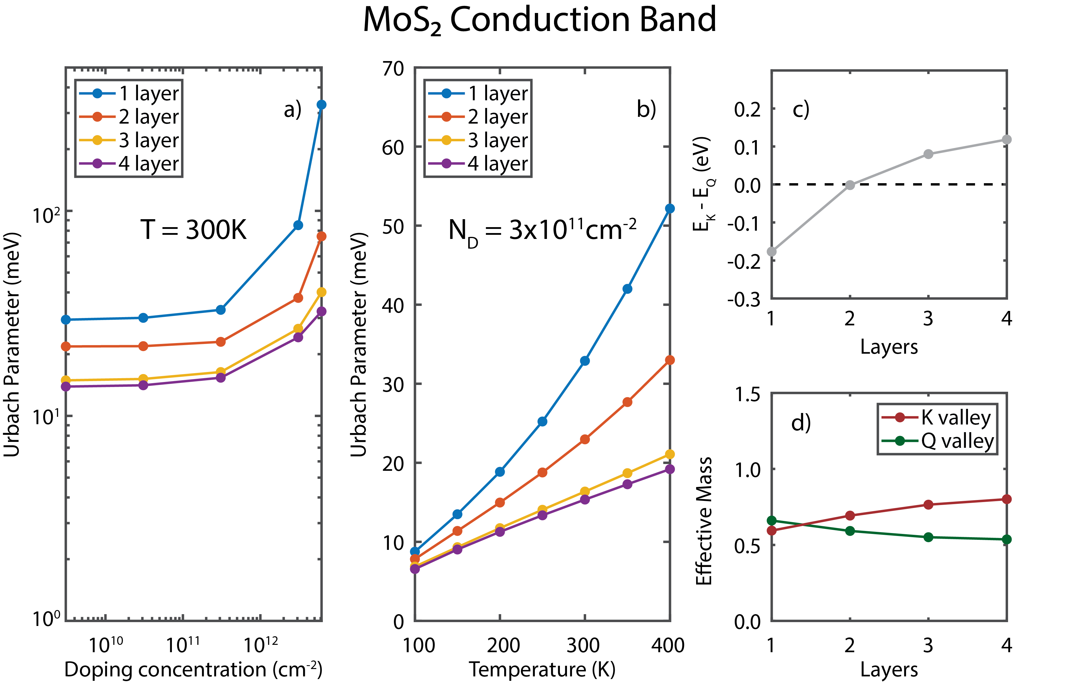
The conduction band of MoS2 has a similar dependence on doping concentration and temperature as the valence band (see Figs. 4 a) and b)). Different to the valence band, however, the conduction band valleys K and Q are degenerate only in the bilayer case (see Fig. 4 c)). In spite of the expected increase in band edge density of states and with it an increase of the conduction band Urbach parameter of the bilayer MoS2, the Urbach parameter shows a monotonous decrease with the number of MoS2 layers (see Figs. 4 a) and b)). This is due to a significant reduction of the calculated scattering self-energy prefactor of polar optical phonon scattering from monolayer to bilayer MoS2 (see table 1). Overall, the conduction band Urbach parameters of MoS2 layers are lower than those of the valence band due the lower conduction band effective masses (see Fig. 4 d)).
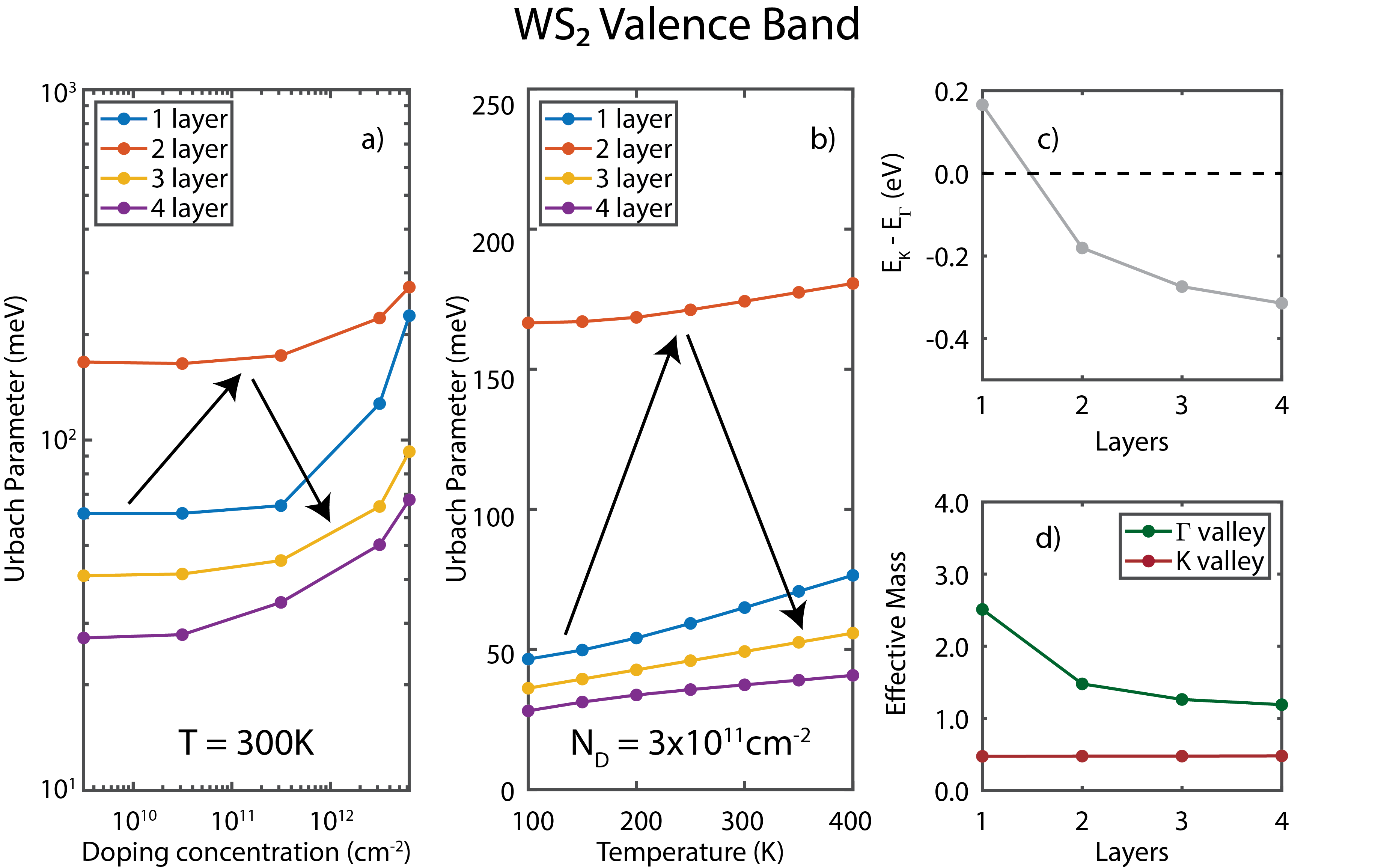
The valence band Urbach parameters of WS2 layers in Figs. 5 a) and b) show similar changes with doping concentration and temperature as the MoS2 valence band results of Figs. 3). However, the Urbach parameter is largest for bilayer WS2. This is due to a transition of the valence band edge from K to valley when more than one layer of WS2 is present (see Fig. 5 c)). Given the large difference of K and valley effective masses (see Fig. 5 d)), this transition causes a maximum in the valence band edge density of states and therefore (as discussed above) a maximum in the scattering strength for bilayer WS2. Accordingly the Urbach parameter follows this trend (indicated with arrows in Figs. 5 a) and b). WS2 with more than 2 layers show the similar reduction in the Urbach parameter as discussed already for MoS2 in Figs. 3.
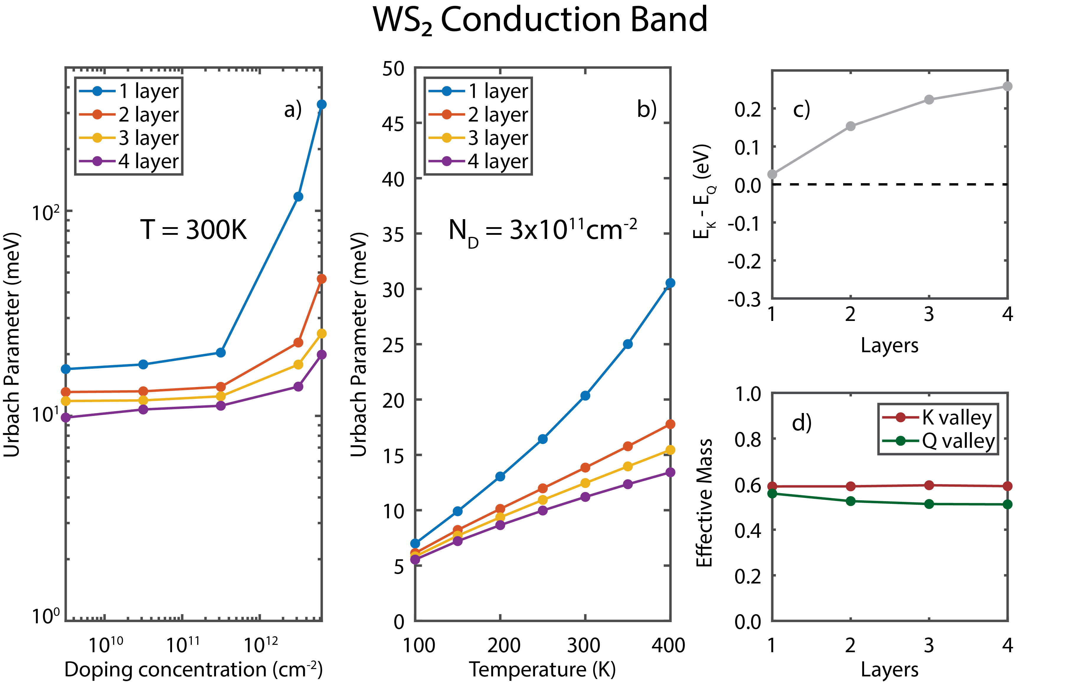
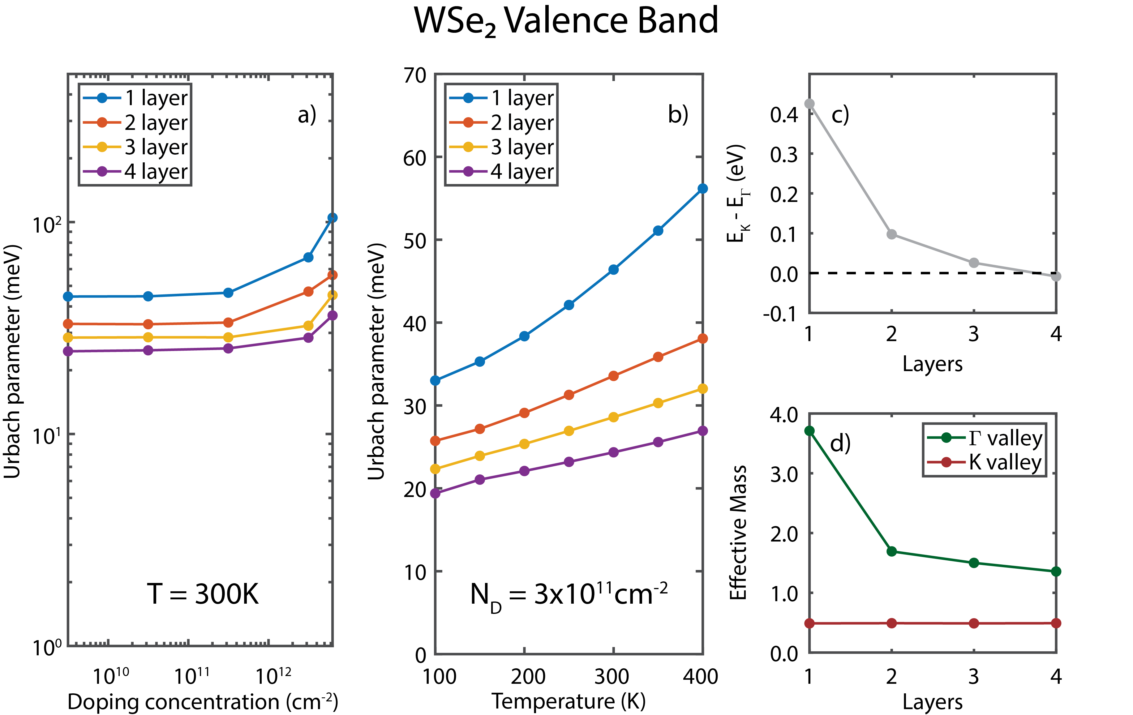
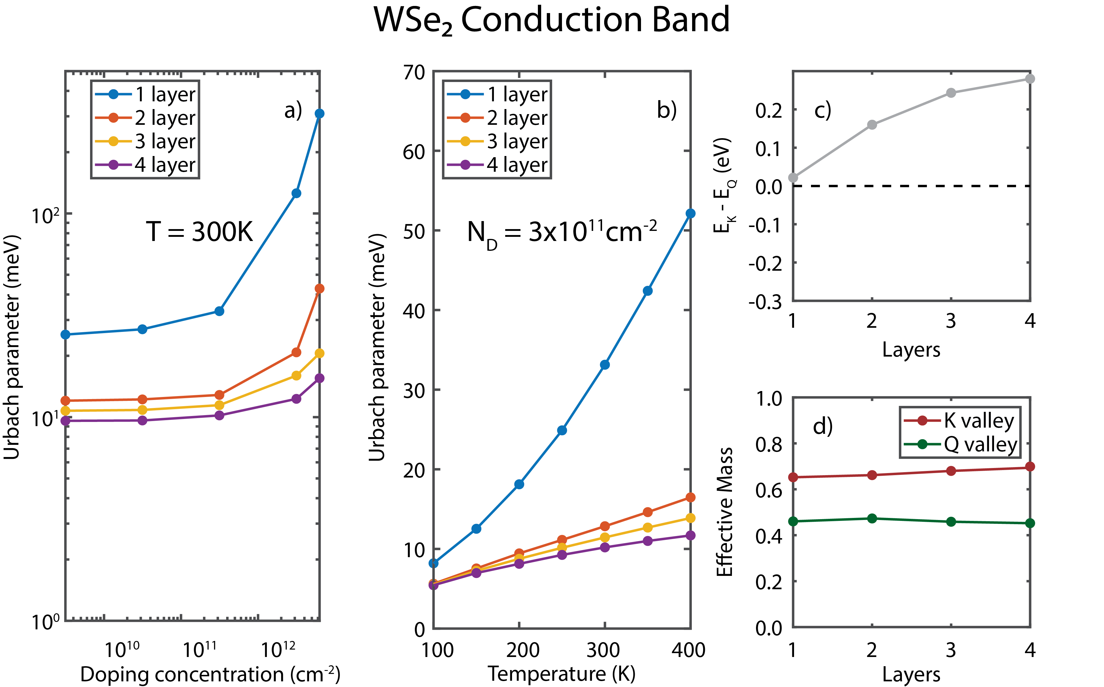
The conduction band Urbach parameter of WS2 (see Figs. 6) is very similar to the one of MoS2 (see Figs. 4) in its overall dependence on doping and temperature. The scattering potential of conduction band of WS2 and with it the Urbach parameter decays with the number of layers (see table 1). Neither significant effective mass changes nor valley degeneracies influence this behavior for WS2 conduction bands. The same is true for valence and conduction bands of WSe2 layers (see Supplementary Figs. 10 and 11).
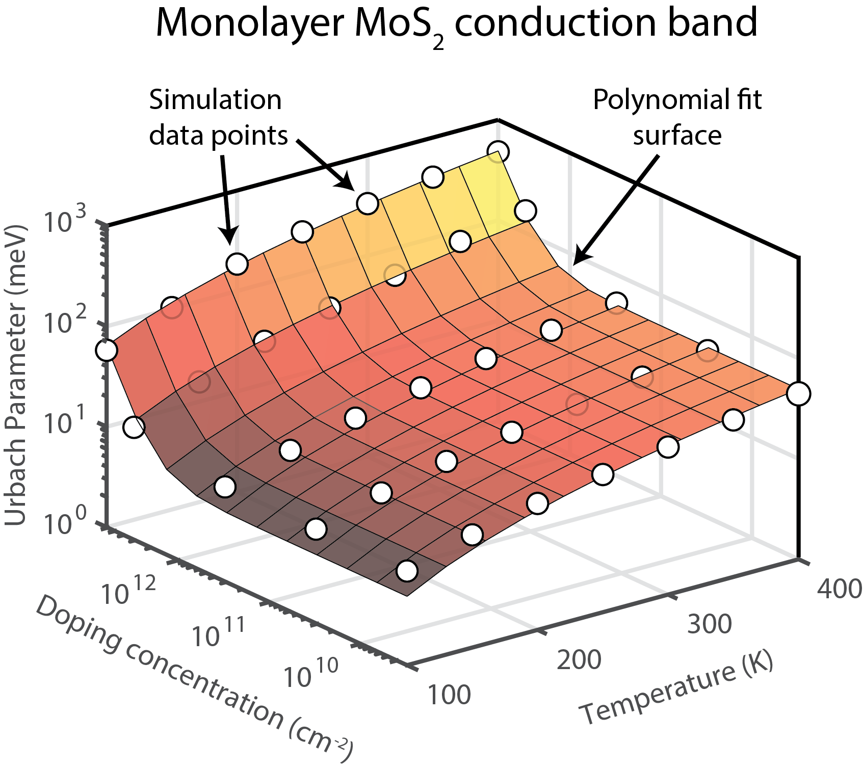
For completeness and to ease estimating the Urbach parameter as a function of doping concentration, temperature, layer thickness and material, all calculated Urbach parameters have been input to a polynomial fit given by
| (6) |
Figure 7 exemplifies this fit for the conduction band Urbach parameter of MoS2. Since the Urbach parameter depends non-monotonically on the number of layers, the least-square fitting is performed for each layer separately. The fit parameters of all consider TMD systems together with their fit values can be found in table 3.
III.2 Band tails: Impacted by dielectric materials
In typical TMD based nanodevices, the TMD layers are capped with dielectric materials. The remote scattering on phonons in those dielectric materials contribute significantly to the Urbach band tail, as shown in Fig. 8.

The relative impact of remote phonon scattering on phonons in the dielectric materials is directly proportional to the scattering self-energy prefactor listed in table 2. This prefactor is determined by the difference of the dielectric constants and the energies of the soft optical phonon modes (see Eq. 2). It is worth to mention, HfO2 has a large scattering impact given its high difference in dielectric constants and the comparably low soft optical phonon mode energies. Following the same arguments, the low scattering contributions of hBN and SiO2 originate in their high phonon mode energies and small difference in their dielectric constants.
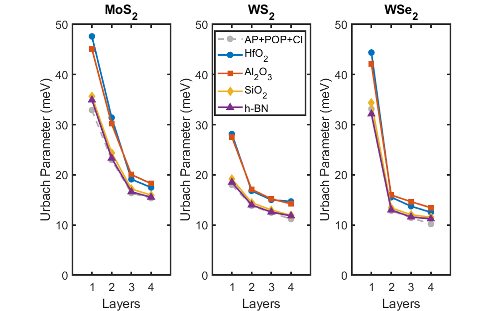
Figure 9 shows the RP scattering impacts the Urbach parameter more in thinner TMD systems than in the thicker ones. This is due to the smaller spatial confinement in larger TMD systems which allows the charge density in the TMD layers to move farther away from the insulator-TMD interface. Accordingly, the difference in the contributions of the various insulators decreases with increasing TMD thickness. Beyond 3 layers, the Urbach parameter starts to saturate and slowly approaches the intrinsic value of the respective TMD. As seen already in Fig. 8, the Urbach parameters are consistently higher for Al2O3 and HfO2 due to their strong RP scattering potentials.
IV Conclusion
Quantum transport calculations of electrons in TMD systems are used to predict the formation of band tails due to scattering on phonons, charged impurities and remote scattering on substrate dielectric phonons. All materials are atomically resolved, electronic Hamiltonian operators are based on DFT, and incoherent, non-local scattering is modeled in self-consistent Born approximation. It is shown that the Urbach band tail parameter strongly depends on temperature, impurity concentration and TMD layer thickness as well as on the type of dielectric substrate. The details of the Urbach parameter depend on a balance of valley degeneracies, scattering potentials and phonon occupancies. This can result in non-monotonic behavior of the Urbach parameter as seen e.g. in WS2. To ease reproducibility of the sophisticated quantum transport calculations, we present analytical approximations to the observed Urbach parameter predictions. Among the dielectric materials considered, Al2O3 and HfO2 are shown to contribute strongest to the remote phonon scattering enhanced band tails. With increasing TMD layer count, electrons spread farther away from the dielectric and thus the contribution of remote scattering on dielectric phonons decreases.
V Acknowledgements
James Charles and Tillmann Kubis acknowledge support by the Silvaco Inc. This research was supported in part through computational resources provided by Information Technology at Purdue, West Lafayette, Indiana. The authors acknowledge the Texas Advanced Computing Center (TACC) at The University of Texas at Austin for providing HPC resources that have contributed to the research results reported within this paper. This research used resources of the Oak Ridge Leadership Computing Facility, which is a DOE Office of Science User Facility supported under Contract DEAC05-00OR22725. Prasad Sarangapani would like to acknowledge Purnima Padmanabhan for helping with the figures.
VI Supplementary Information
| Band Type | Layers | fit value | ||||||
| Valence | 1 | 149.57 | 61.162 | 0.1461 | 0.8073 | 0.9078 | 0.9955 | |
| 2 | 82.981 | 39.460 | 0.1116 | 0.73851 | 0.6793 | 0.9978 | ||
| 3 | 50.096 | 14.623 | 0.1014 | 1.3003 | 0.4714 | 0.9817 | ||
| 4 | 49.101 | 0.1101 | 0.1002 | 3.7729 | 2.3337 | 0.9271 | ||
| Conduction | 1 | 30.567 | 5.7612 | 1.6752 | 1.4527 | 2.1574 | 0.9965 | |
| 2 | 22.461 | 2.4506 | 1.0747 | 1.6788 | 1.6752 | 0.9988 | ||
| 3 | 15.368 | 2.9972 | 0.8734 | 0.0885 | 1.1907 | 0.9923 | ||
| 4 | 48.497 | 1.8010 | 0.0590 | 6.5438 | 0.3661 | 0.9009 | ||
| Valence | 1 | 63.210 | 11.144 | 0.4238 | 1.3126 | 1.5879 | 0.9951 | |
| 2 | 172.43 | 18.337 | 0.1102 | 0.4899 | 0.8087 | 0.9222 | ||
| 3 | 40.343 | 12.360 | 0.2296 | 0.9083 | 0.4475 | 0.9848 | ||
| 4 | 27.545 | 13.102 | 0.1408 | 0.8728 | 0.5770 | 0.9782 | ||
| Conduction | 1 | 17.814 | 15.216 | 1.4801 | 1.0604 | 1.6482 | 0.9982 | |
| 2 | 13.449 | 1.2230 | 0.7822 | 0.8175 | 1.8035 | 0.9970 | ||
| 3 | 12.046 | 1.3597 | 0.7226 | 0.0675 | 1.2610 | 0.9930 | ||
| 4 | 10.196 | 1.0997 | 0.4620 | 0 | 1.2088 | 0.9721 | ||
| Valence | 1 | 45.762 | 4.3223 | 0.3396 | 1.0847 | 1.4928 | 0.9797 | |
| 2 | 33.271 | 0.8838 | 0.2733 | 0 | 1.1190 | 0.9129 | ||
| 3 | 28.843 | 0.0825 | 0.2060 | 3.0934 | 2.8990 | 0.9810 | ||
| 4 | 24.699 | 0.5682 | 0.2214 | 1.7593 | 1.6473 | 0.9564 | ||
| Conduction | 1 | 28.203 | 18.465 | 1.4141 | 1.0200 | 1.4832 | 0.9990 | |
| 2 | 12.450 | 1.0889 | 0.7411 | 0.8994 | 1.8314 | 0.9936 | ||
| 3 | 10.684 | 2.1195 | 0.6217 | 0 | 0.8655 | 0.9917 | ||
| 4 | 9.2162 | 1.6687 | 0.3946 | 0 | 0.7384 | 0.9311 |
References
- Novoselov et al. (2005) K. Novoselov, D. Jiang, F. Schedin, T. Booth, V. Khotkevich, S. Morozov, and A. Geim, Proceedings of the National Academy of Sciences 102, 10451 (2005).
- Wang et al. (2012) Q. H. Wang, K. Kalantar-Zadeh, A. Kis, J. N. Coleman, and M. S. Strano, Nature nanotechnology 7, 699 (2012).
- Jariwala et al. (2014) D. Jariwala, V. K. Sangwan, L. J. Lauhon, T. J. Marks, and M. C. Hersam, ACS nano 8, 1102 (2014).
- Mak and Shan (2016) K. F. Mak and J. Shan, Nature Photonics 10, 216 (2016).
- Manzeli et al. (2017) S. Manzeli, D. Ovchinnikov, D. Pasquier, O. V. Yazyev, and A. Kis, Nature Reviews Materials 2, 17033 (2017).
- Desai et al. (2016) S. B. Desai, S. R. Madhvapathy, A. B. Sachid, J. P. Llinas, Q. Wang, G. H. Ahn, G. Pitner, M. J. Kim, J. Bokor, C. Hu, et al., Science 354, 99 (2016).
- Podzorov et al. (2004) V. Podzorov, M. Gershenson, C. Kloc, R. Zeis, and E. Bucher, Applied Physics Letters 84, 3301 (2004).
- Liu et al. (2011) L. Liu, S. B. Kumar, Y. Ouyang, and J. Guo, IEEE Transactions on Electron Devices 58, 3042 (2011).
- Huyghebaert et al. (2018) C. Huyghebaert, T. Schram, Q. Smets, T. K. Agarwal, D. Verreck, S. Brems, A. Phommahaxay, D. Chiappe, S. El Kazzi, C. L. de la Rosa, et al., in 2018 IEEE International Electron Devices Meeting (IEDM) (IEEE, 2018) pp. 22–1.
- Cheng et al. (2014) R. Cheng, D. Li, H. Zhou, C. Wang, A. Yin, S. Jiang, Y. Liu, Y. Chen, Y. Huang, and X. Duan, Nano letters 14, 5590 (2014).
- Baugher et al. (2014) B. W. Baugher, H. O. Churchill, Y. Yang, and P. Jarillo-Herrero, Nature nanotechnology 9, 262 (2014).
- Zhou et al. (2018) X. Zhou, X. Hu, J. Yu, S. Liu, Z. Shu, Q. Zhang, H. Li, Y. Ma, H. Xu, and T. Zhai, Advanced Functional Materials 28, 1706587 (2018).
- Gu et al. (2019) J. Gu, B. Chakraborty, M. Khatoniar, and V. M. Menon, Nature Nanotechnology 14, 1024 (2019).
- Bie et al. (2017) Y.-Q. Bie, G. Grosso, M. Heuck, M. M. Furchi, Y. Cao, J. Zheng, D. Bunandar, E. Navarro-Moratalla, L. Zhou, D. K. Efetov, et al., Nature nanotechnology 12, 1124 (2017).
- Zheng et al. (2018) W. Zheng, Y. Jiang, X. Hu, H. Li, Z. Zeng, X. Wang, and A. Pan, Advanced Optical Materials 6, 1800420 (2018).
- Tsai et al. (2014) M.-L. Tsai, S.-H. Su, J.-K. Chang, D.-S. Tsai, C.-H. Chen, C.-I. Wu, L.-J. Li, L.-J. Chen, and J.-H. He, ACS nano 8, 8317 (2014).
- Dasgupta et al. (2017) U. Dasgupta, S. Chatterjee, and A. J. Pal, Solar Energy Materials and Solar Cells 172, 353 (2017).
- Yang et al. (2014) X. Yang, W. Fu, W. Liu, J. Hong, Y. Cai, C. Jin, M. Xu, H. Wang, D. Yang, and H. Chen, Journal of Materials Chemistry A 2, 7727 (2014).
- Wang et al. (2017) K.-C. Wang, T. K. Stanev, D. Valencia, J. Charles, A. Henning, V. K. Sangwan, A. Lahiri, D. Mejia, P. Sarangapani, M. Povolotskyi, et al., Journal of Applied Physics 122, 224302 (2017).
- Pospischil and Mueller (2016) A. Pospischil and T. Mueller, Applied Sciences 6, 78 (2016).
- Memaran et al. (2015) S. Memaran, N. R. Pradhan, Z. Lu, D. Rhodes, J. Ludwig, Q. Zhou, O. Ogunsolu, P. M. Ajayan, D. Smirnov, A. I. Fernandez-Dominguez, et al., Nano letters 15, 7532 (2015).
- Lee et al. (2014) C.-H. Lee, G.-H. Lee, A. M. Van Der Zande, W. Chen, Y. Li, M. Han, X. Cui, G. Arefe, C. Nuckolls, T. F. Heinz, et al., Nature nanotechnology 9, 676 (2014).
- Zhang et al. (2016a) W. Zhang, Q. Wang, Y. Chen, Z. Wang, and A. T. Wee, 2D Materials 3, 022001 (2016a).
- Yu and Sivula (2017) X. Yu and K. Sivula, Current Opinion in Electrochemistry 2, 97 (2017).
- Wu et al. (2019) K. Wu, H. Ma, Y. Gao, W. Hu, and J. Yang, Journal of Materials Chemistry A 7, 7430 (2019).
- Das et al. (2019) S. Das, D. Pandey, J. Thomas, and T. Roy, Advanced Materials 31, 1802722 (2019).
- Park et al. (2020) S. Park, Y. Jeong, H.-J. Jin, J. Park, H. Jang, S. Lee, W. Huh, H. Cho, H. G. Shin, K. Kim, et al., ACS nano 14, 12064 (2020).
- Cao et al. (2020) G. Cao, P. Meng, J. Chen, H. Liu, R. Bian, C. Zhu, F. Liu, and Z. Liu, Advanced Functional Materials , 2005443 (2020).
- Wang et al. (2019) L. Wang, W. Liao, S. L. Wong, Z. G. Yu, S. Li, Y.-F. Lim, X. Feng, W. C. Tan, X. Huang, L. Chen, et al., Advanced Functional Materials 29, 1901106 (2019).
- Halperin and Lax (1966) B. Halperin and M. Lax, Physical Review 148, 722 (1966).
- Sarangapani et al. (2019) P. Sarangapani, Y. Chu, J. Charles, G. Klimeck, and T. Kubis, Physical Review Applied 12, 044045 (2019).
- Schenk (1998) A. Schenk, Journal of Applied Physics 84, 3684 (1998).
- Sernelius (1986) B. E. Sernelius, Physical Review B 34, 5610 (1986).
- Halperin and Lax (1967) B. Halperin and M. Lax, Physical Review 153, 802 (1967).
- Van Mieghem (1992) P. Van Mieghem, Reviews of modern physics 64, 755 (1992).
- Lu and Seabaugh (2014) H. Lu and A. Seabaugh, IEEE Journal of the Electron Devices Society 2, 44 (2014).
- Agarwal and Yablonovitch (2014) S. Agarwal and E. Yablonovitch, IEEE Transactions on Electron Devices 61, 1488 (2014).
- Bizindavyi et al. (2018) J. Bizindavyi, A. S. Verhulst, Q. Smets, D. Verreck, B. Sorée, and G. Groeseneken, IEEE Journal of the Electron Devices Society 6, 633 (2018).
- Hebig et al. (2016) J.-C. Hebig, I. Kuhn, J. Flohre, and T. Kirchartz, ACS Energy Letters 1, 309 (2016).
- Ikhmayies and Ahmad-Bitar (2013) S. J. Ikhmayies and R. N. Ahmad-Bitar, Journal of Materials Research and Technology 2, 221 (2013).
- Guerra et al. (2016) J. Guerra, J. Angulo, S. Gomez, J. Llamoza, L. Montañez, A. Tejada, J. Töfflinger, A. Winnacker, and R. Weingärtner, Journal of Physics D: Applied Physics 49, 195102 (2016).
- Beckers et al. (2019) A. Beckers, F. Jazaeri, and C. Enz, IEEE Electron Device Letters 41, 276 (2019).
- Beckers et al. (2021) A. Beckers, D. Beckers, F. Jazaeri, B. Parvais, and C. Enz, Journal of Applied Physics 129, 045701 (2021).
- John et al. (1986) S. John, C. Soukoulis, M. H. Cohen, and E. Economou, Physical review letters 57, 1777 (1986).
- Jain and Roulston (1991) S. Jain and D. Roulston, Solid-State Electronics 34, 453 (1991).
- Zhang et al. (2016b) H. Zhang, W. Cao, J. Kang, and K. Banerjee, in Electron Devices Meeting (IEDM), 2016 IEEE International (IEEE, 2016) pp. 30–3.
- (47) M. L. Van de Put, G. Gaddemane, S. Gopalan, and M. V. Fischetti, in 2020 International Conference on Simulation of Semiconductor Processes and Devices (SISPAD) (IEEE) pp. 281–284.
- Jena and Konar (2007) D. Jena and A. Konar, Physical review letters 98, 136805 (2007).
- Amani et al. (2015) M. Amani, D.-H. Lien, D. Kiriya, J. Xiao, A. Azcatl, J. Noh, S. R. Madhvapathy, R. Addou, K. Santosh, M. Dubey, et al., Science 350, 1065 (2015).
- Fang et al. (2014) H. Fang, C. Battaglia, C. Carraro, S. Nemsak, B. Ozdol, J. S. Kang, H. A. Bechtel, S. B. Desai, F. Kronast, A. A. Unal, et al., Proceedings of the National Academy of Sciences 111, 6198 (2014).
- Jirauschek and Kubis (2014) C. Jirauschek and T. Kubis, Applied Physics Reviews 1, 011307 (2014).
- Eliashberg (1960) G. Eliashberg, Sov. Phys. JETP 11, 696 (1960).
- Kumar and Ahluwalia (2012) A. Kumar and P. Ahluwalia, Physica B: Condensed Matter 407, 4627 (2012).
- Ma and Jena (2014) N. Ma and D. Jena, Physical Review X 4, 011043 (2014).
- Szabó et al. (2015) Á. Szabó, R. Rhyner, and M. Luisier, Physical Review B 92, 035435 (2015).
- Afzalian (2021) A. Afzalian, npj 2D Materials and Applications 5, 1 (2021).
- Charles et al. (2016) J. Charles, P. Sarangapani, R. Golizadeh-Mojarad, R. Andrawis, D. Lemus, X. Guo, D. Mejia, J. E. Fonseca, M. Povolotskyi, T. Kubis, et al., Journal of Computational Electronics 15, 1123 (2016).
- Lemus et al. (2020) D. A. Lemus, J. Charles, and T. Kubis, Journal of Computational Electronics 19, 1389 (2020).
- Khayer and Lake (2011) M. A. Khayer and R. K. Lake, Journal of Applied Physics 110, 074508 (2011).
- Lake et al. (1997) R. Lake, G. Klimeck, R. C. Bowen, and D. Jovanovic, Journal of Applied Physics 81, 7845 (1997).
- Markussen et al. (2009) T. Markussen, A.-P. Jauho, and M. Brandbyge, Physical Review B 79, 035415 (2009).
- Lee and Wacker (2002) S.-C. Lee and A. Wacker, Physical Review B 66, 245314 (2002).
- Kubis et al. (2009) T. Kubis, C. Yeh, P. Vogl, A. Benz, G. Fasching, and C. Deutsch, Physical Review B 79, 195323 (2009).
- Sarangapani et al. (2018) P. Sarangapani, C. Weber, J. Chang, S. Cea, M. Povolotskyi, G. Klimeck, and T. Kubis, IEEE Transactions on Nanotechnology (2018).
- Chu et al. (2019) Y. Chu, J. Shi, K. Miao, Y. Zhong, P. Sarangapani, T. Fisher, G. Klimeck, X. Ruan, and T. Kubis, arXiv preprint arXiv:1908.11578 (2019).
- Geng et al. (2018) J. Geng, P. Sarangapani, K.-C. Wang, E. Nelson, B. Browne, C. Wordelman, J. Charles, Y. Chu, T. Kubis, and G. Klimeck, physica status solidi (a) 215, 1700662 (2018).
- Wang et al. (2020) K.-C. Wang, R. Grassi, Y. Chu, S. Hari Sureshbabu, J. Geng, P. Sarangapani, X. Guo, M. Townsend, and T. Kubis, Journal of Applied Physics 128, 014302 (2020).
- Hafner (2008) J. Hafner, Journal of computational chemistry 29, 2044 (2008).
- Bucko et al. (2010) T. Bucko, J. Hafner, S. Lebegue, and J. G. Angyán, The Journal of Physical Chemistry A 114, 11814 (2010).
- Marzari and Vanderbilt (1997) N. Marzari and D. Vanderbilt, Physical review B 56, 12847 (1997).
- Thygesen et al. (2005) K. S. Thygesen, L. B. Hansen, and K. W. Jacobsen, Physical Review B 72, 125119 (2005).
- Das et al. (2017) R. Das, S. K. Pandey, and P. Mahadevan, arXiv preprint arXiv:1702.04535 (2017).
- Wacker (2002) A. Wacker, Physics Reports 357, 1 (2002).
- Esposito et al. (2009) A. Esposito, M. Frey, and A. Schenk, Journal of computational electronics 8, 336 (2009).
- Mahan (2013) G. D. Mahan, Many-particle physics (Springer Science & Business Media, 2013).
- Jacoboni (2010) C. Jacoboni, Theory of electron transport in semiconductors: a pathway from elementary physics to nonequilibrium green functions, Vol. 165 (Springer Science & Business Media, 2010).
- Fischetti et al. (2001) M. V. Fischetti, D. A. Neumayer, and E. A. Cartier, Journal of Applied Physics 90, 4587 (2001).
- Lindhard (1954) J. Lindhard, Dan. Vid. Selsk Mat.-Fys. Medd. 28, 8 (1954).
- Sancho et al. (1985) M. L. Sancho, J. L. Sancho, J. L. Sancho, and J. Rubio, Journal of Physics F: Metal Physics 15, 851 (1985).
- Jin et al. (2014) Z. Jin, X. Li, J. T. Mullen, and K. W. Kim, Physical Review B 90, 045422 (2014).
- Ridley (2013) B. K. Ridley, Quantum processes in semiconductors (Oxford university press, 2013).
- The MathWorks (2019) I. The MathWorks, Curve Fitting Toolbox, Natick, Massachusetts, United State (2019).