Performance of a High Power and Capacity
Mobile SLIPT Scheme
Abstract
The increasing demands of power supply and data rate for mobile devices promote the research of simultaneous wireless information and power transfer (SWIPT). Optical SWIPT, as known as simultaneous light information and power transfer (SLIPT), has the potential for providing high-capacity communication and high-power wireless charging. However, SLIPT technologies based on light-emitting diodes have low efficiency due to energy dissipation over the air. Laser-based SLIPT technologies need strict positioning accuracy and scanning resolution, which may lead to the increase of costs and complexity. In this paper, we propose a mobile SLIPT scheme based on spatially separated laser resonator (SSLR) and intra-cavity second harmonic generation. The power and data are transferred via separated frequencies, while they share the same self-aligned resonant beam path, without the needs of receiver positioning and beam steering. We establish the analysis model of the resonant beam power and its second harmonic power. Numerical results show that the proposed system can achieve watt-level battery charging power and above -bit/s/Hz achievable rate at -m distance, which satisfies the requirements of most indoor mobile devices.
Index Terms:
spatially-distributed laser, resonant beam, laser communications, wireless power transfer, 6G.I Introduction
The increasing demands of virtual reality (VR), augmented reality (AR), and other bandwidth-consuming services bring many challenges to conventional mobile networks, including radio frequency spectrum crisis and fast battery depletion. Simultaneous wireless information and power transfer (SWIPT) technology is an attractive way to cope with these challenges, as it can provide sustainable power supply through the communication link [1]. In the sixth-generation (6G) mobile network, SWIPT service is highly expected [2]. The final form of mobile network can be completely different from what we are experiencing today [3].
SWIPT using radio-frequency (RF) carrier has been well-studied. RF wave can provide a large coverage area, non-line-of-sight (NLoS) transmission, low scattering and absorption in atmosphere, and mature manufacturing; hence, it has many application scenarios such as wireless sensor network distributed in a large area. However, the shortage of RF spectrum resources limits the development of the RF-based SWIPT. Owing to high communication bandwidth, simultaneous light information and power transfer (SLIPT) has arisen much attention. Freespace optical communications (FSO) technologies have the potential to support over Tbit/s data rate [4], which points out the promising prospect of SLIPT. Paper [5] presented a novel SLIPT, in which a solar cell is employed for energy harvesting (EH) and a photodiode (PD) is used for information detection. The SLIPT system presented in [6] splits the direct-current (DC) energy and the alternating-current (AC) information signal from the received power by a separator; it is also optimized with new strategies and policies for the balance of the trade-off between EH and the quality of service (QoS). The work in [7] presented a promising relaying SLIPT system with rate optimization, in which the powers for EH and communication are split directly by a power splitter. Paper [8] investigated the use of VLC links for simultaneous lighting, communications, and energy harvesting. Paper [9] investigated the sum rate maximization problem in a downlink SLIPT system and proposed a low-complexity iterative algorithm. Performance comparison between RF-based SWIPT and SLIPT was carried out in [10], which demonstrated the superior performance of SLIPT. The transmitters employed in these SLIPT systems are-light emitting diodes (LEDs).
However, transmitters with isotropic antennas or LEDs exhibit very low transmission efficiency due to the path loss over the large divergence angle. For example, an isotropic antenna operating at MHz and supplied with W can only transfer W to the receiver at -m distance [11]. From LED radiation within coverage angle, the receiver can only obtain -mW electric power at -m distance [12]. Therefore, for power-hungry devices, narrow-beam carrier is preferred. For instance, Iyer et al. demonstrated a safeguard-beam-based laser power transfer system which can safely deliver over -W electrical power at a range of m [13]. Rizzo et al. employed -W -nm laser as the transmitter, achieving -W electrical output at the receiver [14]. Furthermore, hybrid optical wireless power and data transmission system is also introduced in [15], which employed two laser diodes at different frequencies to transfer power and information independently; this experimental work achieved received optical power and -MHz bandwidth. These laser-based optical SWIPT technologies have to obtain the position of the receiver and then direct the laser beam to the receiver. Although beam steering can be realized by many non-mechanical devices, such as two-dimensional (2D) fiber arrays [16], in-fiber diffraction gratings [17], optical phased arrays (OPAs) [18], crossed gratings [19], and spatial light modulators (SLMs) [20], the strict needs of positioning accuracy and scanning resolution may lead to the increase of costs and complexity, especially for long-range transmission [21]. Particularly, for watt-level laser transfer, inaccurate positioning and insensitive detection will lead to dangerous events.
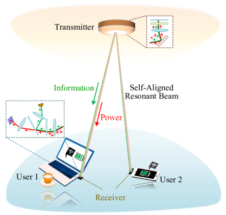
Resonant beam generated by spatially separated laser resonator (SSLR) can be used for mobile optical SWIPT without the requirements of positioning and beam steering, as shown in Fig. 1. Recently, high-power mobile wireless charging using resonant beam was proposed in [22], which is known as resonant beam charging (RBC) or distributed laser charging (DLC). Experiment on RBC was demonstrated in [23], which received -W electrical power at -m distance. Resonant beam communication (RBCom) system with high-capacity channel was illustrated in [24]. The primary structure of SSLR origins from Lindford’s very long laser cavity which has two oppositely-placed corner cube retroreflectors [25]. The safety of the SSLR was verified in [26]. The SSLR also has limitations with respect to communications, as the signal inside the cavity bounces back and forth, leading to echo interference. To address the echo interference issue, SSLR structures with external-cavity second harmonic generation (SHG) and intra-cavity SHG are proposed in [27] and [28], respectively. However, [27] and [28] only consider information transfer, ignoring the ability of the resonant beam in power transfer. [29] and [30] investigated a SWIPT system based on corner-cube-based SSLR and cat’s-eye-based SSLR, respectively, while they transfer information and power via the same wavelength, and split the power proportionally at the receiver. In this case, the modulation applied to the beam reduces the charging power, and hence, the power loss in this process is inevitable. Moreover, they did not address the echo interference issue.
In this paper, we propose a resonant beam SWIPT (RB-SWIPT) system based on SSLR and intra-cavity SHG. In addition to the aforementioned advantages of the RBC and RBCom system in power, mobility, and capacity, the RB-SWIPT system separates the communication beam from the power transfer beam (i.e., the resonant beam) at the transmitter and converts them into signal and electricity at the receiver independently using a PD and a photovoltaic panel (PV).
The contributions of our work are as follows.
-
1)
We propose the SHG-based RB-SWIPT system to provide a high-power and high-capacity mobile transmission channel, and design an structure for optical frequency-splitting transmission and independent conversion. In this design, the modulation is only applied to the information transfer beam, and thus, it cannot affect the power transfer beam, which avoids extra power loss.
-
2)
We establish the coupling model of the resonant beam power and its second harmonic power and analyze the performance of the RB-SWIPT system on the received charging power and achievable rate.
The remainder of this paper is organized as follows. Section II presents the system design of the RB-SWIPT system. Section III illustrates the system analysis model. Section IV demonstrates the results of performance evaluation. Section V discusses the concerns on safety, energy efficiency, and misalignment. Finally, we conclude in Section VI.
II The Proposed System
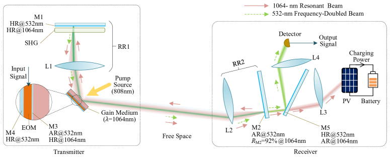
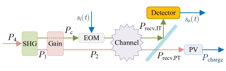
The SWIPT system is based on the SSLR and SHG scheme presented in [28]. As demonstrated in Fig. 2, power is transferred via -nm resonant beam, while information is transferred via -nm frequency-doubled beam. The frequency-doubled beam is generated from the resonant beam by an SHG crystal and modulated by an electro-optic modulator (EOM). At the receiver, part of the resonant beam is allowed to pass through mirror M2, and then is focused on the PV by lens L3. At last, the extracted resonant beam is converted into current by the PV to charge the battery. The frequency-doubled beam passes through M2, and then is separated from the resonant beam by a dichroic mirror M5; and finally, it is focused on the PD by lens L4 and converted into current signal by the PD.
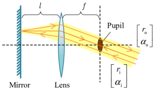
The resonant beam is generated inside the SSLR cavity. The SSLR consists of two TCRs RR1 and RR2 which are placed at the transmitter and the receiver, respectively. Retroreflectors are devices to reflect the incident beam back to its incoming direction. Therefore, photons inside the SSLR cavity can oscillate between RR1 and RR2 regardless of the retroreflectors’ location, as long as these TCRs are in each other’s field of view (FOV). Generally, a TCR consists of a lens and a rear mirror which are formed coaxially and separated with a space. The ray-transfer matrix of the telecentric cat’s eye retroreflector is expressed as [28]
| (1) |
and
| (2) |
where is the focal length of the lens, and is the interval between the lens and the mirror. If , represents an ideal TCR. The ray-transfer matrix of an optical system is used to calculate the position and the transfer direction of the output ray from those of the input ray. Given the vector, , of the input ray of the ideal TCR, we can obtain the vector of the output ray; that is
| (3) |
where () and () are the transverse displacement and the angle of the input (output) ray, respectively, with respect to the optical axis. From (3), we can see that the output ray is parallel to the input ray, as shown in Fig. 3. Nevertheless, in SSLR, should be a little greater than to ensure a stable resonator, which is illustrated in the following section. TCR has a pupil located at the focal point of the lens. Only the beams that pass through the pupil of the TCR can be retro-reflected. Therefore, the intra-cavity resonant beam always passes through the pupils of RR1 and RR2. We place the gain medium at the pupil of RR1, so that the resonant beam can always reach the gain medium regardless of the location of the receiver, as long as the receiver is in the FOV of the transmitter, and vice versa. Similarly, the EOM is placed behind the gain medium, so that the frequency-doubled beam can always reach the EOM.
In this paper, we employ an neodymium-doped yttrium orthovanadate (Nd:YVO4) crystal as the gain medium. This material can amplify -nm light under the irradiation of -nm pump source light. It can also be pumped with -nm light, which helps reduce the heat dissipation, but a thicker crystal is needed to compensate for the decreased absorption coefficient. The choice of the pump wavelength depends on the FOV requirement and the heat-sinking capability. As the gain medium absorbs the pump power, the atoms at the lower energy level transit to the the upper level continuously, providing the stimulated emission capability. The intra-cavity resonant beam oscillating between RR1 and RR2 is amplified by the gain medium through the stimulated emission. In the stimulated emission transition of an excited atom at the upper level, an extra photon identical to the input one is generated, and meanwhile, the excited atom transits to the lower level. Since the loss of the resonant beam is compensated by the gain, the resonance in the cavity can be maintained. Much heat is generated by the gain medium, so it is important to design the heat sink well. For example, we can use indium piece to fill the gap between the gain medium (with the EOM) and the heat sink. For high-power pump, a cooling module is helpful for the heat dissipation. SHG crystals are devices to generate frequency-doubled beam from a fundamental beam. In this system, the fundamental beam for SHG is the resonant beam. We place the SHG crystal inside RR1 and make it parallel to the rear mirror. Because beams that enter through the pupil of the TCR are perpendicular to the rear mirror, they have the same incident angle to the SHG crystal. This feature meets the phase-matching requirement of the SHG crystal.
Various anti-reflective (AR), high-reflective (HR), and partial-reflective coatings at different wavelengths are employed. M1 is coated with HR coating at nm. M2 is coated with partial-reflective coating at nm. Hence, M1 and M2 capture most of the resonant beam power. Only a small part of the resonant beam power is released by M2 for battery charging. The back side of the gain medium is coated with HR coating at nm to prevent the resonant beam passing through and being changed by the EOM; and it is also coated with AR coating at nm to allow the frequency-doubled beam going into the EOM. M1 and the back side of the EOM are coated with HR coatings at nm to reflect the frequency-doubled beam. M2 is coated with AR coating at nm to allow the frequency-doubled beam going out of the cavity, preventing any possible intra-cavity oscillation at nm. The front side of M5 is coated with HR coating at nm and AR coating at nm, so that M5 can separate the two wavelengths. Besides, the two sides of each lens and the SHG crystal, the input plane of the detector and the PV, and the back side of M5 are coated with AR coatings at both nm and nm to prevent unnecessary reflection.
III System Analysis
The proposed SWIPT system has two branches, i.e., the power transfer (PT) branch and the information transfer (IT) branch. In this section, we at first introduce the mechanism of resonant beam generation, and present the necessary condition for a stable SSLR. Then, the process of communication carrier generation is illustrated. At last, the photoelectric conversion and battery charging as well as the detection of the information signal are described.
III-A Resonant Beam Generation
In our system, the power is transferred via the resonant beam whose frequency is . As shown in Fig. 4(a), the resonant beam is generated between M1 and M2. In this work, we only consider that RR1 and RR2 have exactly the same parameters, including the same focal length and the same space interval . The beam radius varies along the -axis. The SSLR can be expressed by a single-pass ray-transfer matrix, which is also called the ABCD matrix; that is [27]
| (4) |
where is the transmission distance that is defined as the space interval between the pupils of RR1 and RR2. The elements of ABCD matrix can be used to analyze the stability of resonators [31, 32]. Let and , we can use the condition to judge the stability of the SSLR. Here, using expressed in (2), we can know that the stable-cavity condition is . Note that the real distance also depends on the losses in the cavity. Moreover, high temperature at the gain medium will result in thermal lens, which will reduce the range of stable regime. Therefore, a cooling system design for the gain medium is important.
The components of the ABCD matrix can also be used to estimate the beam radius at arbitrary location along the optical axis. We should at first obtain the -parameter and then use it to calculate the beam radius. There are multiple transverse modes included in the resonant beam; and their superposition determines the radius of the resonant beam. The modes that can be included in a resonant beam are determined by the apertures of the optical devices in the cavity. Among these modes, the fundamental mode TEM00 exhibits the smallest radius. We can obtain the radius of the fundamental mode at location by [33]
| (5) |
where takes the imaginary part of a complex number, and is the wavelength of the resonant beam. The parameter is computed by [27]
| (6) |
where , , , , and are the locations of lens L1, lens L2, lens L3, and PV, respectively. Note that L3 and L4 are symmetric about M5. Also, the positions of the PD and the PV are symmetric about M5. From (6), we can observe that is divided into three parts along -axis. All the -parameters are derived from . In fact, the -parameters at one side of an optical element is derived from the -parameters at the other side using the transfer-matrix method.
The ratio of the beam radius to the TEM00 mode radius is a constant along the -axis. This ratio is called the beam propagation factor. To compute the beam radius at arbitrary location , we can firstly obtain the resonant beam radius and the TEM00 mode radius at the gain medium and then calculate the beam propagation factor. Since the aperture of the gain medium has the smallest aperture among the devices inside the cavity, we can consider that high-order modes whose radius is greater than the gain medium aperture are blocked, while only those with smaller radius remain in the cavity. Therefore, we can make a good approximation that , where is the radius of the gain medium aperture [33]. Then the beam radius at location can be computed by
| (7) |
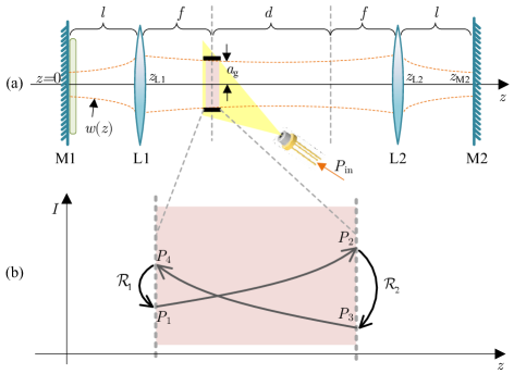
Next, we calculate the power of the resonant beam. The light wave bounces in the SSLR circularly, where the resonant beam power varies during transferring inside the SSLR. According to the Rigrod analysis, we can calculate the power at each stage, as depicted in Fig 4(b). Here, we create an equivalent resonator for this calculation, and assume that the beam radius in the gain medium is a fixed value. The equivalent resonator only contains two equivalent mirrors and a gain medium, as shown in Fig. 4(b). The reflectivity of the equivalent mirrors are and . Then, the power of the incident beam at the left-side equivalent mirror is obtained by [34]
| (8) |
where and are the voltage reflection coefficients of the equivalent mirrors, is the saturation intensity, is the gain medium thickness, is the combined pumping efficiency, is the gain medium volume, and is the electric power for driving the pump source. combines the power attenuation induced by the SHG and RR1. combines the power attenuation induced by the gain medium, the air, and RR1. They are expressed as
| (9) |
where is the SHG efficiency which represents the consumption of the resonant beam power in the SHG process; is the transmittance of the SHG crystal without considering the loss induced by the SHG process; and are the loss factors of RR1 and RR2, respectively; is the transmittance of the gain medium; is the transmittance of the air, where m-1 for clear air; is the diffraction loss factor which can be approximated by a closed-from formula presented in [27]. is induced by the losses of passing through lens L1 and mirror M1. These losses mainly include the reflection of the surfaces of the lenses and the transmission of the mirrors, which are inevitable. Let denote the transmittance of L1, and denote the reflectivity of M1, the loss factor of RR1 is expressed as
| (10) |
Similarly, the loss factor of RR2 is expressed as
| (11) |
where is the transmittance of lens L2, and is the reflectivity of mirror M2.
Now we have the expression of the resonant beam power outputting from the left-side surface of the gain medium. Since the SHG efficiency is a function of , we should solve the following equations to obtain the actual value of :
| (12) |
where is the vacuum permeability; is the speed of light; , , and are the SHG crystal’s efficient nonlinear coefficient, thickness, and refractive index, respectively [35, 36]. Here, we assume the input of the SHG crystal is a plane wave. This is valid when is smaller than the Rayleigh length . Under this assumption, the beam radius is constant along the axis in the SHG crystal. represents the resonant beam intensity that contains the leftward- and rightward-traveling wave at the SHG crystal. We also assume is small, where the intensities of the leftward- and the rightward-traveling waves at the SHG crystal are the same. This condition can be satisfied because the communication demand for the carrier beam power is very small. There is no analytic solution for (12). Hence, we obtain the numerical solution using MATLAB.
III-B Communication Carrier Generation
The SHG process is based on the nonlinear phenomenon of birefringent crystals, in which the crystal absorbs two fundamental photons and then generates a frequency-doubled photon. In our system, the resonant beam photons at frequency are the fundamental photons of the SHG process. Thus, the frequency-doubled photons have the frequency of . The communication carrier is the superposition of the frequency-doubled beams that generated from the leftward- and the rightward-traveling components of the resonant beam. Since the frequency of the communication carrier exhibits higher energy than that of the stimulated absorption band of the gain medium atoms, the frequency-doubled beam can not interfere resonant beam generation. Thus, the resonant beam and the communication carrier transfer independently. At the receiver, the communication carrier is separated from the resonant beam by the frequency-selective coating of the dichroic mirror M5. This is easy to be realized, as the frequency difference between the communication carrier and the resonant beam is up to THz. Consequently, the effect of the dichroic mirror on the signal bandwidth can be neglected. With the aforementioned low-SHG-efficiency assumption, the carrier beam power is approximated as
| (13) |
Many materials, such as lithium niobate (LiNbO3), potassium titanyl phosphate (KTP), and potassium dihydrogen phosphate (KDP), can be employed for this purpose. Different materials exhibit different nonlinear coefficients and different phase matching angles. The incident angle of the input beam at the SHG crystal should be coincident with the phase matching angle to reach the maximum conversion efficiency. Since the beams between M1 and L1 are always perpendicular to these devices, a fixed beam incident angle at the SHG crystal can be satisfied. Hence, the crystal can be cut with proper orientation to ensure that the beam incident angle equals the phase matching angle. We choose LiNbO3 as an example in this paper, since it can provides zero walk-off angle at -nm incident wavelength [35]. In fact, with the development of manufacturing, many advanced materials can be produced for this particular application.
III-C Communication Channel and Achievable Rate
As depicted in Fig. 2 and Fig. 5, the carrier is modulated by the EOM, transmitted through the channel, extracted by the dichroic mirror M5, and finally received by the detector. Along the transmission path, the signal is attenuated by the lenses, the mirrors, the gain medium, the EOM, and the air. These loss factors are caused by non-ideal reflection, non-ideal transmission, or absorption of impurity. Hence, the received optical power for information transfer is expressed as
| (14) |
where , , , , , are the transmittances of mirror M2, lens L1, lens L2, lens L4, the combined body of the gain medium and the EOM, and the air, respectively; is the reflectivity of mirror M5; the superscript represents that the operating frequency is ; and represents the ratio of power received by the PD to the total incident power. Generally, PD has a contractor on the front of the detecting area, which expands its receiving area to an effective signal collection area . Let denote the beam cross section area, the receiving ratio is expressed as:
| (15) |
The expression of is given as [37]
| (16) |
where is the concentrator gain, is the transmissivity of the concentrator surface, is the incidence angle with respect to the receiver axis, and is the semi-angle FOV of the concentrator. The expression of is given as [37]
| (17) |
where is the internal refractive index of the concentrator. Since the branches of IT and PT are symmetric around M5, the received beam cross section area, , at PD is also approximated by (7).
From the received optical power to electric current, the conversion ratio is denoted by , which is usually called the PD’s responsivity. Here we only consider the dominant noises, namely, the shot noise and the thermal noise. They are additive white Gaussian noise (AWGN). The optical communication channel with intensity modulation is known as free-space optical intensity channel. Here, represents the peak signal power that can be received. Generally, as a result of power consumption and safety consideration, there is an average power restriction for the intensity channel. The real average power depends on the modulation and encoding schemes. In our system, we assume the ratio of the average received power to the peak received power lies in the range of , as the energy resources and the safety are not significant restrictions in our system. Then, we find the achievable rate by computing the lower-bounded channel capacity; that is [38]
| (18) |
where is the nature constant. is the noise variance, which is obtained as [39]
| (19) |
where is the electron charge, is Boltzmann constant, A is the photon current induced by background radiation [40], is the bandwidth, is the temperature in Kelvin, and is the load resistance. The optical devices on the transmission path of the modulated beam are passive components. The light frequency of the communication carrier is up to THz. The signal bandwidth is much smaller than the carrier frequency. Thus, these passive optical devices have less effect to the signal bandwidth. Generally, the system bandwidth is limited by the EOM and the PD. There are several kinds of spatial EOMs, such as piezoelectric thin films [41] and multiple quantum well (MQW) modulators [42]. Typical bandwidth of spatial EOMs is MHz to several gigahertzs. Some commercial PDs provide up to -GHz bandwidth [43, 44, 45]. The actual bandwidths of the EOM and the PD depend on their incident areas. But the limitation of the incident area can be addressed by arrays structure [46, 47].
III-D Charging Power at Receiver
At the power transfer branch, the power of the traveling wave (at frequency ) outputting from the right-side surface of the gain medium (see Fig. 4) is transferred through the channel and received by the PV panel. Similar to the information transfer branch, the beam power experiences a series of attenuation induced by the air, the optical devices, and the PV. Therefore, the received optical power for wireless charging is expressed as
| (20) |
where , , and are the transmittances of lens L2, lens L3, mirror M2, and mirror M5, respectively; the superscript represents that the specified operating frequency is ; and represents the percentage of the received power of the PV in the arrived PT beam power, not including the part that is reflected off the PV’s receiving plane, as well as the part that is lost due to the limited size of the receiving area. All of these factors attenuate the beam power when the PT beam passes these components. As shown in Fig. 4(b), the power and come from the amplified and , respectively; and the power and come from the attenuated and , respectively. Thus, the following relations can be obtained:
| (21) |
We also know that the production of the leftward- and the rightward-traveling waves at arbitrary location in the -axis is a constant, namely [34]
| (22) |
By combining these relations expressed in (21) and (22), we can obtain
| (23) |
where and are roots of and , respectively; and their expressions are given in (12). Consequently, the received optical power at the power transfer branch can be expressed as
| (24) |
| Parameter | Symbol | Value |
|---|---|---|
| Focal length of the lens | cm | |
| Interval between the lens and mirror | cm | |
| Saturation intensity of the gain medium | W/m2 | |
| Resonant beam wavelength | nm | |
| Radius of gain medium aperture | mm | |
| Gain medium thickness | mm | |
| Combined pumping efficiency | ||
| Efficient nonlinear coefficient | pm/V | |
| Refractive index of SHG crystal | 2.23 | |
| SHG crystal thickness | mm | |
| PV’s responsivity | A/W | |
| Reverse saturation current | A | |
| Shunt resistance | ||
| Series resistance | m | |
| Diode ideality factor | ||
| Number of cells in PV panel | ||
| Temperature | K | |
| PD’s responsivity | A/W | |
| Load resistor | k |
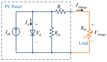
The received optical power at the PV panel is converted into electricity for battery charging. As demonstrated in Fig. 6, the PV panel can be equivalent to a current source in parallel with a diode. The current generated by the source is called the photo-current , which is expressed as
| (25) |
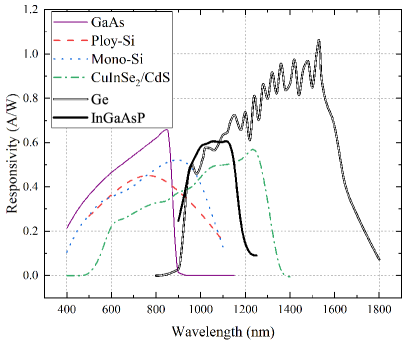
where is the optical-to-electrical conversion responsivity. However, for real devices, there are a shunt resistance and a series resistance inside the PV model. Different photoelectronic material at different wavelength exhibits different responsivity. Fig. 7 shows the spectral response curves of different materials, including gallium arsenide (GaAs) [48], polycrystalline silicon (Poly-Si) [49], monocrystalline silicon (Mono-Si) [50], copper indium selenium/cadmium sulfide (CuInSe2/CdS) [51], germanium (Ge) [52], and indium gallium arsenide phosphide (InGaAsP) [53]. According to Kirchhoff’s law, we can write down the following equations for this circuit model; that is [54, 55]
| (26) |
where is the current passing through the diode; is the voltage on the diode; is the reverse saturation current; is Boltzmann’s constant; is the diode ideality factor; and is the number of cells connected in series in the PV panel. In this paper, we only consider single-cell PV panel, i. e., . We also obtain the numeric solution of (26), as it has no analytical solution.
For a certain , the PV panel performs like a constant-current source unless the output voltage approaches the open-circuit voltage. The PV can achieve a maximum power point (MPP) if we chose a proper charging voltage. Generally, this work is implemented by a maximum power point tracking (MPPT) device connected to the battery. To obtain the maximum charge power , we solve the following problem
| (27) | ||||
| (30) |
In (30), is the equivalent load resistance of the circuit connected to the PV panel. It is the MPPT device that adjusts the load resistance automatically to find the MPP. is called the open-circuit voltage, which is the output voltage of the PV panel when no load circuit is connected.
IV Numerical Results
IV-A Parameters Setting
Unless otherwise specified, the parameters of our system are listed in Table I. In this paper, an Nd:YVO4 crystal is used as the gain medium. Hence, the wavelength of the resonant beam nm, and the information carrier is the -nm frequency-doubled beam. Nd:YVO4 is an efficient crystal for diode-pump solid-state lasers. It has large stimulated emission cross-section at lasing wavelength and high absorption coefficient at pumping wavelength. Thus, the crystal can be cut into a thin disk to satisfy the FOV requirement of our system. The parameters of the gain medium material are obtained from [35], including the saturation intensity , the stimulated wavelength , and the combined pump efficiency .
The parameters of the SHG material are also obtained from [35], including the efficient nonlinear coefficient and the refractive index . The shape parameters of the gain medium and the SHG medium are customized in this paper according to the requirements. In our SSLR-based wireless charging experiment, the diameters of the lenses and mirrors are mm [23]. Since the apertures of the lenses and mirrors are much bigger than the gain medium, their effects can be neglected in calculation. These lenses and mirrors are made of N-BK7 glasses. Here, the focal length of each lens is set as cm. The space interval between the lens and the mirror in each TCR is set as cm. Then, is calculated as m, and thus, the upper boundary of the distance is m.
For devices through which the beams pass, including the lenses, the SHG crystal, and the dichroic mirror, unwanted reflection at their input and output surfaces exists even if these devices are with the best production. We set the transmittance at each AR surface as which is a typical value of commercial products. Therefore, we set . Also the receiving surfaces of PD and PV have reflectivity of ; hence, we set . The receiving area of such high-speed PD should be [47]. We set the semi-angle FOV of the PD as and the refractive index of concentrator as [56]. The incidence angle . HR mirrors/coatings also have inevitable transmittance; hence, we set their real reflectivity . As the resonant beam passes the gain medium, it meets the front AR surface twice and the back HR surface once. Therefore, we set . The frequency-doubled beam meets interfaces five time as it passes the combined body of the gain medium and the EOM. Hence, we set . Besides, we set the bandwidth MHz which is a feasible value of electro-absorption modulators [46]. From the spectral response curves shown in Fig. 7, we found that InGaAsP performs well at nm (responsivity is about A/W), while GaAs has a good responsivity ( A/W) at nm. Therefore, we choose InGaAsP and GaAs as the materials of PV and PD, respectively. Other manufacturing-dependent parameters for PD and PV are obtained from [40] and [57], respectively.
IV-B Performance Evaluation
Fig. 8 demonstrates the maximum charging power achieved by the MPPT device as a function of the reflectivity of the mirror M2, for different source power . As increases, gradually increases to a maximum point and then decreases to . The maximum value of can be obtained with a specific . Moreover, as grows, the optimal value of appears slightly decreasing. We also evaluate the achievable rate . As depicted in Fig. 8, with the increase of , increases rapidly at first; and when reaches a large value, the change of gradually slows down. When W and , reaches the maximum value, i.e., W; in this case, bit/s/Hz.
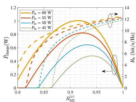
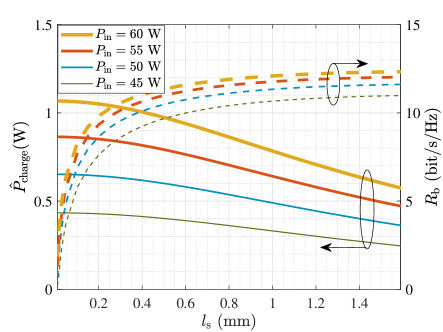
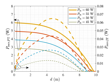
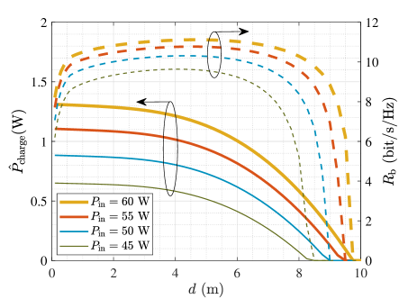
Fig. 9 depicts the maximum charging power and the achievable rate as a function of the SHG crystal thickness , for different source power . According to (12), the thickness of the SHG crystal affects the SHG efficiency . As shown in Fig. 9, as increases, increases rapidly at first and then gradually approaches the highest point. This is because increases with , and thus more frequency-doubled photons are generated. Conversely, the intra-cavity resonant beam power decreases gradually with the increase of , leading to the decrease of .
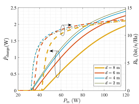
We analyzed the received PT beam power and IT beam power at difference transmission distance , as shown in Fig. 10. is at watt-level, while has several tens of milliwatts. With the increase of the distance, decreases with a slow speed at first, and the decrease speed increases gradually. However, with the increase of the distance, increases at first. This phenomenon can be explained by the decrease of the beam radius at the SHG crystal with the growth of distance, which results in the increasing resonant beam intensity and SHG efficiency. When m, turns to decrease due to the increase of the diffraction loss. In addition, we analyzed the changes of the maximum charging power and the achievable rate with the distance , as shown in Fig. 11. As increases, decreases gradually. However, the achievable rate grows smoothly over most of the transmission range. When W and the distance is less than m, keeps above W, which is suitable for most indoor charging scenarios. For example, a typical mobile phone which is charged with V and A (i.e., the charge power is W) can be fully charged from to for hour. When we use the RB-SWIPT system, the phone can be fully charged within hours. Although the charging time is extended, the phone can be charged in use or in idle time, without the disturbing of cables. Similarly, keeps above bit/s/Hz within a large range of distance. Only when the distance is less than m or greater than m does decrease rapidly to zero.
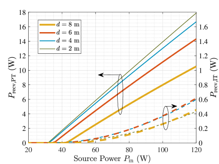
As depicted in Fig. 12, the relation between the received PT beam power and the pump source power is linear. However, as grows, the increase of accelerates. This is because the resonant beam intensity at the SHG crystal is also increased, which leads to the increase of the SHG efficiency. There is a threshold of for each case. If is below the threshold, the resonance can not be established, and thus the received powers are zeros. As shown in Fig. 13, the maximum charging power and the achievable rate also depend on . After exceeds the threshold, and start to increase. grows rapidly as exceeds the threshold, and quickly reaches a slow growth rate. For a large range of , rate can achieve over bit/s/Hz. As continues to increase, the growth rate of reduces gradually. This phenomenon can be explained by the decreased PV efficiency with the increase of the incident optical power. From Fig. 13, we can also observe that, by choosing an appropriate , the RB-SWIPT system can achieve watt-level battery charging power and over -m distance. The above performance can support most indoor mobile devices with permanent battery life and high-quality multimedia stream transmission.
V Discussion
V-A Safety
Both skin safety and eye safety should be considered when implementing a resonant beam system. Laser products have been classified into seven classes according to the international electrotechnical commission (IEC) standards IEC 60825-1 and IEC 60825-12 [58]. For eye safety under long-time exposure, the product should satisfy the maximum exposure energy (MPE) restriction of Class 1 and Class 1M. This depends on not only the power density on the eyes but also the wavelength and the size of the source, i.e., it depends on whether the source in the eye’s view is a point source or an extended source. As shown in Fig. 14, there are spontaneous emission and stimulated emission in the resonant beam system. The spontaneous emission is omnidirectional. When the resonance has not been initiated or has been interrupted by obstacles, many excited atoms (have absorbed the pump power) in the gain medium lie at the higher energy level, and they transit to the lower energy level by emitting photons spontaneously. The stimulated emission (i.e., the resonant beam) is directional, as it occurs relying on the intra-cavity resonance and the optical amplification.
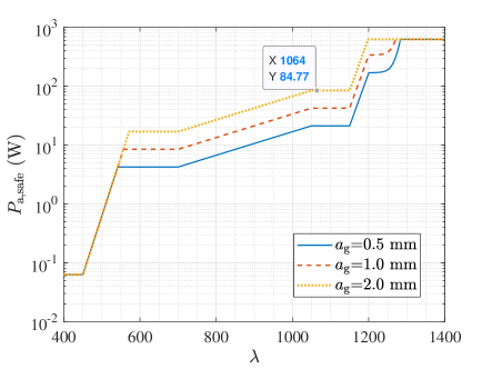
Now, we discuss the safety of these two cases. Since the spontaneous emission is omnidirectional and the gain medium diameter mm, the gain medium is classified as an extended source, as defined in IEC 60825 [59]. According to the standard, the MPE of Class I extend source with radius (angular of subtense mrad) and nm is computed as W/cm2. If the input source power to the pump diode is W, the actual power absorbed by the gain medium, , should be obtained by multiplying and a series of efficiencies, including the pump source efficiency , the pump laser transmission efficiency , and the gain medium absorption efficiency [35]; that is W. Since there is an HR coating behind the gain medium, the real spontaneous emission power intensity at the most restrictive measurement distance cm is approximated as W/cm2, which is under the MPE value. Different wavelengths have different MPE values. The maximum permissible absorbed powers under different and are depicted in Fig. 15. We can see that W under the parameters specified in this paper. Then the maximum permissible source power is calculated as W. To verify the eye safety of real products, rigorous measurements and ethical animal experiments are still needed. Hence, it is necessary to wear a protective glasses for working wavelengths during the laser experiment.
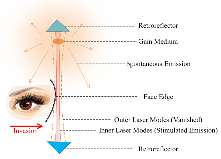
In fact, when the stimulated emission becomes dominant, the power of spontaneous emission reduces largely. This gives us the opportunity to reduce the spontaneous emission by adjusting the pump progress. Namely, we can use a low source power to generate the resonant beam and detect the resonance by a sensor. Only when the resonance is detected do we further increase the source power. Besides, using wavelengths greater than nm can reduce the risk of retina injury as these wavelengths are absorbed by the vitreous humor in eyes.
The stimulated emission can not reach the eyes, as it is interrupted by the obstruction of human face. The resonant beam is very thin, generally with millimeter-level radius, and it consists of many transverse modes. From high-order to low-order modes, the mode radius decreases. Those modes oscillate in the cavity independently. When a human face is entering the resonant beam, the mode with the greatest radius vanish first due to the increase of the diffraction loss. The power is then reallocated to the inner oscillating modes. This energy transfer process continues as the human face invasion process progresses. The interval between the edges of two adjacent modes are less than mm, and the ratio of the energy outside the mode radius to the total mode energy is less than . Even though the diffraction energy of the outer modes is released on the face edge, the power reaching the eyes is negligible. In addition, as the overlap between the resonant beam and the gain medium becomes small due to the vanishing of outer modes, the power used for stimulated emission is decreased, leading to the decrease of the resonant beam power.
Quantitatively analysis with light-field simulation on the diffraction energy received by an invading object is demonstrated in [26], which verified the skin safety of the resonant beam system under the given parameters. We also experimentally verified the skin safety of the resonant beam system driven by -W pump laser, as presented in [23]. Parameter optimization can help reduce the power exposure during intrusion. For instance, improving the gain of the gain medium and correspondingly decreasing the reflectivity, , of the output mirror M2 can reduce the intra-cavity beam power and meanwhile keep the output power unchanged. This principle may motivate new designs for the resonant beam system, including the SSLR structure, the gain medium material, and the pump module structure.
V-B Energy Efficiency
Recently, the energy efficiency in this paper is around (only consider the PT branch; W; m). The power losses occur in several steps: ① electro-optical conversion of pump laser diode, ② pump laser transmission, ③ gain medium absorption, ④ spontaneous emission and ⑤ nonradiative transition of excited atoms, ⑥ diffraction loss during beam propagation, ⑦ passing the intra-cavity optical devices, ⑧ over-the-air transmission, and ⑨ photovoltaic conversion. In this work, the parameters of the pump source module and the gain medium are obtained from the experiment conducted in [35]. However, with the development of technologies, the laser devices have been constantly improved. For example, if the gain medium is pumped directly with electricity, referring to vertical-cavity surface-emitting lasers (VECSELs) [60], the power losses in the pump process (steps ① – ③, contributing to 32.4% power loss) can be removed. Loss in step ④ can be reduced by adjusting the active shape of the gain medium (for example, using VECSEL arrays), which can improve the overlap efficiency. Loss in step ⑤ depends on the gain medium material, which generates heat. The pump frequency also affects this efficiency. For instance, nm for Nd:YVO4 generates less heat than nm. The diffraction loss in step ⑥ is very small in our cavity, as the SSLR operates in the stable regime; yet, the radius of the optical devices should be much greater than the TEM00 mode radius, which is easy to be satisfied. The transmittance of each optical element with AR coatings is up to . Although it is hard to further improve the optical elements, reducing the intra-cavity beam power (decreasing the output mirror reflectivity and meanwhile improving the gain medium amplification) can also reduce the energy consumption (in steps ⑥ – ⑧) of the intra-cavity optical components. The energy consumption of the air in step ⑧ can be neglected in indoor scenario. As for step ⑨, the PV efficiency has been continuously improved in recent years. For such single-wavelength applications, the PV efficiency is reported as up to at nm [61] or at nm [62]. Above all, many losses can be reduced in future by optimizing the system parameters and also by developing new SSLR structures and materials. The overall PT efficiency in future is expected to reach – .
V-C Misalignment
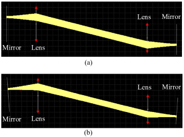
Different from a two-mirror resonator which needs to place the mirrors in parallel, retroreflectors in the SSLR do not need to be aligned as long as they locate in the FOV of the opposite one. The resonant beam is self-aligned between the transmitter and the receiver. As depicted in Fig. 16(a), even if the two retroreflectors are not coaxially placed, rays can be captured by the resonator, forming an intra-cavity beam (ray optics simulation using open source software [63]). The misalignment between the mirror and the lens in a retroreflector is also worth investigating. As shown in Fig. 16(b), the mirrors are tilted, while the rays in the cavity can still be captured. A little misalignment between the lens and the mirror in the retroreflectors does not affect the self-producing capability of the intra-cavity beam, although it changes the FOV of the transmitter and the receiver. The tilt angle of the mirror/lens in each TCR should be as small as possible to ensure a large moving range.
VI Conclusions
In this paper, we proposed a resonant-beam-based simultaneous information and power transfer (RB-SWIPT) system which uses spatially separated laser resonator (SSLR) and second harmonic generation (SHG) to provide a high-power and high-capacity mobile transmission channel. We designed an optical frequency-splitting receiver structure, in which the power and information are transferred independently via the resonant beam and its frequency-doubled beam while sharing the same optical transmission path that is self-aligned without positioning and beam steering. We established the intra-cavity power coupling model of the resonant beam and the frequency doubled beam as well as the power receiving model to estimate the received battery charging power and the achievable rate. Numerical results show that the RB-SWIPT system can achieve watt-level battery charging and over -bit/s/Hz achievable rate at -m distance, which can enable permanent battery life and high-quality multimedia stream transmission of mobile devices in indoor scenarios.
There are still several issues to be addressed in future. For instance, the energy efficiency needs to be improved. Beside, analytical model that considers the incidence angle should be investigated. Furthermore, to improve the performance, a parameter optimization algorithm should be developed.
References
- [1] L. R. Varshney, “Transporting information and energy simultaneously,” in IEEE International Symposium on Information Theory, Toronto, ON, Canada, July 2008, pp. 1612–1616.
- [2] K. David and H. Berndt, “6G vision and requirements: Is there any need for beyond 5G?” IEEE Veh. Technol. Mag., vol. 13, no. 3, pp. 72–80, July 2018.
- [3] T. D. Ponnimbaduge Perera, D. N. K. Jayakody, S. K. Sharma, S. Chatzinotas, and J. Li, “Simultaneous wireless information and power transfer (SWIPT): Recent advances and future challenges,” IEEE Commun. Surveys Tuts., vol. 20, no. 1, pp. 264–302, Dec. 2018.
- [4] E. Ciaramella, Y. Arimoto, G. Contestabile, M. Presi, A. D’Errico, V. Guarino, and M. Matsumoto, “1.28-Tb/s (32 40 Gb/s) free-space optical WDM transmission system,” IEEE Photon. Technol. Lett., vol. 21, no. 16, pp. 1121–1123, Aug. 2009.
- [5] S. Ma, F. Zhang, H. Li, F. Zhou, Y. Wang, and S. Li, “Simultaneous lightwave information and power transfer in visible light communication systems,” IEEE Trans. Wireless Commun., vol. 18, no. 12, pp. 5818–5830, Dec. 2019.
- [6] P. D. Diamantoulakis, G. K. Karagiannidis, and Z. Ding, “Simultaneous lightwave information and power transfer (SLIPT),” IEEE Trans. Green Commun. Netw., vol. 2, no. 3, pp. 764–773, Sept. 2018.
- [7] S. Ma, F. Zhang, H. Li, F. Zhou, Y. Wang, and S. Li, “Simultaneous lightwave information and power transfer in visible light communication systems,” IEEE Trans. Wireless Commun., vol. 18, no. 12, pp. 5818–5830, Dec. 2019.
- [8] H. G. Sandalidis, A. Vavoulas, T. A. Tsiftsis, and N. Vaiopoulos, “Illumination, data transmission, and energy harvesting: the threefold advantage of VLC,” Appl. Opt., vol. 56, no. 12, pp. 3421–3427, Apr. 2017.
- [9] Y. Li, N. Huang, J. Wang, Z. Yang, and W. Xu, “Sum rate maximization for VLC systems with simultaneous wireless information and power transfer,” IEEE Photon. Technol. Lett., vol. 29, no. 6, pp. 531–534, IEEE 2017.
- [10] S. S. Morapitiya, M. F. Ali, S. Rajkumar, S. K. Wijayasekara, D. N. K. Jayakody, and R. Weerasuriya, “A SLIPT-assisted visible light communication scheme,” in 16th International Conference on Distributed Computing in Sensor Systems (DCOSS), Marina del Rey, CA, USA, May 2020, pp. 368–375.
- [11] T. Le, K. Mayaram, and T. Fiez, “Efficient far-field radio frequency energy harvesting for passively powered sensor networks,” IEEE J. Solid-State Circuits, vol. 43, no. 5, pp. 1287–1302, May 2008.
- [12] P. D. Diamantoulakis and G. K. Karagiannidis, “Simultaneous lightwave information and power transfer (SLIPT) for indoor IoT applications,” in IEEE Global Communications Conference, Singapore, Dec. 2017, pp. 1–6.
- [13] V. Iyer, E. Bayati, R. Nandakumar, A. Majumdar, and S. Gollakota, “Charging a smartphone across a room using lasers,” Proc. ACM Interact. Mob. Wearable Ubiquitous Technol., vol. 1, no. 4, pp. 1–21, Jan. 2017.
- [14] L. Rizzo, K. J. Duncan, J. L. Zunino, and J. F. Federici, “Validation of laser power beaming applications with enlarged laser beam diameters minimizing hazardous operation,” in SoutheastCon, Huntsville, AL, USA, Apr. 2019, pp. 1–5.
- [15] A. W. S. Putra, H. Kato, and T. Maruyama, “Hybrid optical wireless power and data transmission system,” in IEEE PELS Workshop on Emerging Technologies: Wireless Power Transfer (WoW), Seoul, Korea (South), Nov. 2020, pp. 374–376.
- [16] T. Koonen, A. Khalid, J. Oh, F. Gomez-Agis, and E. Tangdiongga, “High-capacity optical wireless communication using 2-dimensional IR beam steering,” in Opto-Electronics and Communications Conference (OECC) and Photonics Global Conference (PGC), Singapore, Nov. 2017, pp. 1–4.
- [17] G. Wang, U. Habib, Z. Yan, N. J. Gomes, Q. Sui, J.-B. Wang, L. Zhang, and C. Wang, “Highly efficient optical beam steering using an in-fiber diffraction grating for full duplex indoor optical wireless communication,” J. Lightw. Technol., vol. 36, no. 19, pp. 4618–4625, Oct. 2018.
- [18] H. Rhee, J. You, H. Yoon, K. Han, M. Kim, B. G. Lee, S. Kim, and H. Park, “32 Gbps data transmission with 2D beam-steering using a silicon optical phased array,” IEEE Photon. Technol. Lett., vol. 32, no. 13, pp. 803–806, May 2020.
- [19] T. Koonen, J. Oh, K. Mekonnen, and E. Tangdiongga, “Ultra-high capacity indoor optical wireless communication using steered pencil beams,” in Proc. International Topical Meeting on Microwave Photonics, Paphos, Cyprus, Oct. 2015, pp. 4802–4809.
- [20] Z. Zhang, J. Dang, L. Wu, H. Wang, J. Xia, W. Lei, J. Wang, and X. You, “Optical mobile communications: Principles, implementation, and performance analysis,” IEEE Trans. Vehi. Technol., vol. 68, no. 1, pp. 471–482, Nov. 2019.
- [21] J. Luo, L. Fan, and H. Li, “Indoor positioning systems based on visible light communication: State of the art,” IEEE Commun. Surveys Tuts., vol. 19, no. 4, pp. 2871–2893, Aug. 2017.
- [22] Q. Liu, J. Wu, P. Xia, S. Zhao, W. Chen, Y. Yang, and L. Hanzo, “Charging unplugged: Will distributed laser charging for mobile wireless power transfer work?” IEEE Veh. Technol. Mag., vol. 11, no. 4, pp. 36–45, Nov. 2016.
- [23] Q. Liu, M. Xiong, M. Liu, Q. Jiang, W. Fang, and Y. Bai, “Charging a smartphone over the air: The resonant beam charging method,” IEEE Internet Things J., Jan 2022, to appear, doi: 10.1109/JIOT.2022.3142031.
- [24] M. Xiong, Q. Liu, G. Wang, G. B. Giannakis, and C. Huang, “Resonant beam communications: Principles and designs,” IEEE Commun. Mag., vol. 57, no. 10, pp. 34–39, Oct. 2019.
- [25] G. J. Linford, E. R. Peressini, W. R. Sooy, and M. L. Spaeth, “Very long lasers,” Appl. Opt., vol. 13, no. 2, pp. 379–390, Feb. 1974.
- [26] W. Fang, H. Deng, Q. Liu, M. Liu, Q. Jiang, L. Yang, and G. B. Giannakis, “Safety analysis of long-range and high-power wireless power transfer using resonant beam,” IEEE Trans. Signal Process., vol. 69, pp. 2833–2843, May 2021.
- [27] M. Xiong, M. Liu, Q. Jiang, J. Zhou, Q. Liu, and H. Deng, “Retro-reflective beam communications with spatially separated laser resonator,” IEEE Trans. Wireless Commun., vol. 20, no. 8, Aug. 2021.
- [28] M. Xiong, Q. Liu, X. Wang, S. Zhou, B. Zhou, and Z. Bu, “Mobile optical communications using second harmonic of intra-cavity laser,” IEEE Trans. Wireless Commun., vol. 21, no. 5, May 2022.
- [29] M. Liu, H. Deng, Q. Liu, J. Zhou, M. Xiong, L. Yang, and G. B. Giannakis, “Simultaneous mobile information and power transfer by resonant beam,” IEEE Trans. Signal Process., vol. 69, pp. 2766–2778, May 2021.
- [30] M. Liu, M. Xiong, Q. Liu, S. Zhou, and H. Deng, “Mobility-enhanced simultaneous lightwave information and power transfer,” IEEE Trans. Wireless Commun., vol. 20, no. 10, pp. 6927–6939, May 2021.
- [31] H. Kogelnik, “Imaging of optical modes — resonators with internal lenses,” Bell Syst. Tech. J., vol. 44, no. 3, pp. 455–494, July 2013.
- [32] P. Baues, “Huygens’ principle in inhomogeneous, isotropic media and a general integral equation applicable to optical resonators,” Opt. Quantum Electron., vol. 1, no. 1, pp. 37–44, Feb. 1969.
- [33] N. Hodgson and H. Weber, Laser Resonators and Beam Propagation: Fundamentals, Advanced Concepts and Applications 2nd ed. New York, NY., U.S.: Springer, 2005.
- [34] A. E. Siegman, Lasers. Mill Valley, CA: University Science Books, 1986.
- [35] W. Koechner, Solid-State Laser Engineering, 6th ed. New York, NY, USA: Springer, 2006.
- [36] U. Simon and F. K. Tittel, “Nonlinear optical frequency conversion techniques,” Exp. Methods Phys. Sci., vol. 29, no. 08, pp. 231–278, Jan. 1997.
- [37] J. M. Kahn and J. R. Barry, “Wireless infrared communications,” Proc. IEEE, vol. 85, no. 2, pp. 265–298, Feb. 1997.
- [38] A. Lapidoth, S. M. Moser, and M. A. Wigger, “On the capacity of free-space optical intensity channels,” IEEE Trans. Inf. Theory, vol. 55, no. 10, pp. 4449–4461, Oct. 2009.
- [39] F. Xu, M. A. Khalighi, and S. Bourennane, “Impact of different noise sources on the performance of PIN- and APD-based FSO receivers,” in Proceedings of the 11th International Conference on Telecommunications, Graz, Austria, June 2012, pp. 211–218.
- [40] A. J. C. Moreira, T. V. Rui, and A. M. de Oliveira Duarte, “Optical interference produced by artificial light,” Wirel. Netw., vol. 3, no. 2, pp. 131–140, May 1997.
- [41] E. Defay, T. Lacrevaz, T. Vo, V. Sbrugnera, C. Bermond, M. Aid, and B. Flechet, “Ferroelectric properties of Pb(Zr,Ti)O3 thin films until 40 GHz,” Appl. Phys. Lett., vol. 94, no. 5, p. 052901, Feb. 2009.
- [42] B. Noharet, Q. Wang, S. Junique, D. Agren, and S. Almqvist, “Multiple quantum-well spatial light modulators for optical signal processing,” in Proc. Integrated Optical Devices, Nanostructures, and Displays, vol. 5618, London, United Kingdom, Nov. 2004, pp. 146–155.
- [43] Y. Salamin, P. Ma, B. Baeuerle, A. Emboras, Y. Fedoryshyn, W. Heni, B. Cheng, A. Josten, and J. Leuthold, “100 GHz plasmonic photodetector,” ACS Photonics, vol. 5, no. 8, pp. 3291–3297, June 2018.
- [44] FINISAR, “100GHz ultra-high speed balanced photodetector,” accessed Mar. 2022. [Online]. Available: https://www.epsglobal.com/Media-Library/EPSGlobal/Products/files/finisar/roadm-fws-optoelectronic/BPDV412xR.pdf?ext=.pdf
- [45] T. Umezawa, K. Akahane, A. Matsumoto, A. Kanno, N. Yamamoto, and T. Kawanishi, “High-responsivity 100GHz waveguide UTC photodetector,” in Broadband Access Communication Technologies XI, vol. 10128, San Francisco, CA, USA, Jan. 2017, p. 1012807.
- [46] C. Quintana, Q. Wang, D. Jakonis, X. Piao, G. Erry, D. Platt, Y. Thueux, A. Gomez, G. Faulkner, and H. Chun, “High speed electro-absorption modulator for long range retroreflective free space optics,” IEEE Photon. Technol. Lett., vol. 29, no. 9, pp. 707–710, May 2017.
- [47] T. Umezawa, A. Matsumoto, K. Akahane, S. Nakajima, and N. Yamamoto, “Large submillimeter high-speed photodetector for large aperture FSO receiver,” IEEE J. Sel. Topics Quantum Electron., vol. 28, no. 2, pp. 1–9, Mar. 2021.
- [48] S. Mintairov, N. Kalyuzhnyy, M. Maximov, A. Nadtochiy, S. Rouvimov, and A. Zhukov, “GaAs quantum well-dots solar cells with spectral response extended to 1100 nm,” Electron. Lett., vol. 51, no. 20, pp. 1602–1604, Oct. 2015.
- [49] S. Kumari, N. Arora, and G. Jain, “Grain size dependence of the photovoltaic properties of solar grade polysilicon,” Sol. Energy Mater., vol. 5, no. 4, pp. 383–390, Oct. 1981.
- [50] E. L. Meyer, M. A. Malape, and M. Simon, “Influence of temperature on photovoltaic cells spectral response,” in 38th IEEE Photovoltaic Specialists Conference, Austin, TX, USA, June 2012, pp. 254–257.
- [51] L. Kazmerski, F. White, and G. Morgan, “Thin-film CuInSe2/CdS heterojunction solar cells,” Appl. Phys. Lett., vol. 29, no. 4, pp. 268–270, Aug. 1976.
- [52] M. Meusel, C. Baur, G. Létay, A. Bett, W. Warta, and E. Fernandez, “Spectral response measurements of monolithic GaInP/Ga(In)As/Ge triple-junction solar cells: measurement artifacts and their explanation,” Prog. Photovolt., vol. 11, no. 8, pp. 499–514, Dec. 2003.
- [53] J. Yin, Y. Sun, S. Yu, Y. Zhao, R. Li, and J. Dong, “1064 nm InGaAsP multi-junction laser power converters,” J. Semicond., vol. 41, no. 6, p. 062303, June 2020.
- [54] J. L. Gray, The Physics of the Solar Cell, 2nd ed. Chichester, UK: John Wiley & Sons Ltd, 2011.
- [55] D. Sera, R. Teodorescu, and P. Rodriguez, “PV panel model based on datasheet values,” in IEEE International Symposium on Industrial Electronics, Vigo, Spain, June 2007, pp. 2392–2396.
- [56] A. Burton, Z. Ghassemlooy, S. Rajbhandari, and S.-K. Liaw, “Design and analysis of an angular-segmented full-mobility visible light communications receiver,” Trans. Emerg. Telecommun. Technol., vol. 25, no. 6, pp. 591–599, Mar. 2014.
- [57] W. Long, T. Wu, J. Jiao, M. Tang, and M. Xu, “Refraction-learning-based whale optimization algorithm for high-dimensional problems and parameter estimation of PV model,” Eng. Appl. Artif. Intell., vol. 89, p. 103457, Mar. 2020.
- [58] M. D. Soltani, E. Sarbazi, N. Bamiedakis, P. de Souza, H. Kazemi, J. M. H. Elmirghani, I. H. White, R. V. Penty, H. Haas, and M. Safari, “Safety analysis for laser-based optical wireless communications: A tutorial,” arXiv e-prints, pp. 1–54, Feb. 2021. [Online]. Available: https://arxiv.org/pdf/2102.08707.pdf
- [59] “Safety of laser products - part 1: Equipment classification, requirements and user’s guide,” International Electrotechnical Commission (IEC) 60825-1:2014 Std., Aug. 2014.
- [60] J. E. Hastie, S. Calvez, M. D. Dawson, T. Leinonen, A. Laakso, J. Lyytikinen, and M. Pessa, “High power CW red VECSEL with linearly polarized TEM00 output beam,” Opt. Express, vol. 13, no. 1, pp. 77–81, Jan. 2005.
- [61] N. A. Kalyuzhnyy, V. M. Emelyanov, V. V. Evstropov, S. A. Mintairov, M. A. Mintairov, M. V. Nahimovich, R. A. Salii, and M. Z. Shvarts, “Optimization of photoelectric parameters of InGaAs metamorphic laser (= 1064 nm) power converters with over 50% efficiency,” Sol. Energy Mater Sol. Cells, vol. 217, p. 110710, Nov. 2020.
- [62] S. Fafard, F. Proulx, M. C. York, L. Richard, P.-O. Provost, R. Arès, V. Aimez, and D. P. Masson, “High-photovoltage GaAs vertical epitaxial monolithic heterostructures with 20 thin p/n junctions and a conversion efficiency of 60%,” Appl. Phys. Lett., vol. 109, no. 13, p. 131107, Sept. 2016.
- [63] “Ray optics simulation,” accessed Mar, 2022. [Online]. Available: https://ricktu288.github.io/ray-optics/