Mn ions’ site and valence in PbTiO3 based on the native vacancy defects
Abstract
Mn ions’ doping site and valence were studied in PbTiO3 (PT) with the native vacancy defects by the first-principles calculations. Firstly, the native vacancy defects of Pb, O and Ti in PT were investigated and it was found that Pb vacancy is preferred to others. And then the growth of Mn doped PT should be preferred to Mn ion substituting for an A-site Pb ion with +3 valence when Pb is deficient under equilibrium conditions driven solely by minimization of the formation energy, and this could result in a larger lattice distortion of PT. In addition, when Mn enters the Pb site, the electronegativity of O becomes weaker which makes the domain movement easier in PT to improve the performance of PT, while Mn ion substitution for a B-site Ti ion is the opposite.
Key words: Mn doping, PT, native defects, defect formation energy, Bader charge
Abstract
Íà îñíîâi ïåðøîïðèíöèïíîãî ìîäåëþâàííÿ âèâчàëèñÿ ìiñöå ëåãóâàííÿ i âàëåíòíiñòü iîíiâ Mn ó ñïîëóêàõ PbTiO3 (ÐÒ) ç ïðèðîäíèìè äåôåêòàìè âàêàíñié. Ñïåðøó áóëè âèâчåíi ïðèðîäíi äåôåêòè âàêàíñié Pb, O òà Ti ó PT, i áóëî âèÿâëåíî, ùî âàêàíñiÿ Pb є íàéêðàùîþ. Ïðè ðîñòi ÐÒ, ëåãîâàíî¿ Mn, ïåðåâàæíèì ìàє áóòè çàìiùåííÿ iîíàìè Mn ç âàëåíòíiñòþ +3 iîíiâ Pb â À-öåíòðàõ, êîëè êîíöåíòðàöiÿ Pb є íåäîñòàòíüîþ â óìîâàõ ðiâíîâàãè. Öå îáóìîâëåíî âèêëþчíî ìiíiìiçàöiєþ åíåðãi¿ óòâîðåííÿ i ìîæå ïðèçâåñòè äî áiëüøî¿ äèñòîðñi¿ ãðàòêè ÐÒ. Êðiì òîãî, êîëè Mn ïîòðàïëÿє íà ìiñöå Pb, åëåêòðîíåãàòèâíiñòü O ñòàє ñëàáøîþ, ùî ïîëåãøóє ðóõ äîìåíiâ â PT i ïîêðàùóє õàðàêòåðèñòèêè öiє¿ ñïîëóêè, òîäi ÿê çàìiùåííÿ iîíàìè Mn iîíiâ Ti â B-öåíòði ìàє ïðîòèëåæíèé åôåêò.
Ключовi слова: ëåãóâàííÿ Mn, ñïîëóêè PT, ïðèðîäíi äåôåêòè, åíåðãiÿ óòâîðåííÿ äåôåêòiâ, çàðÿä Áåéäåðà
1 Introduction
The advantage of lead titanate PbTiO3 (PT) and lead zirconate titanate PbZr1-xTixO3 (PZT) as Pb-based ferroelectric materials, has been well exhibited in infrared pyroelectric sensors, piezoelectric transducers, nonvolatile memories and so on [1, 2, 3, 4]. Furthermore, some cations were also introduced to modify their properties and improve their applications [5, 6, 7, 8, 9, 10, 11, 12, 13, 14, 15]. Mn doped PT and PZT exhibiting different characteristics with dopant concentration have attracted a lot of interest [14, 15, 16, 17, 18]. Especially, Mn can have a softening effect on PT and PZT at a small concentration [14, 16, 17]. It was deemed that the occurrence of a small amount of Mn ions entering the A site was compatible with small differences between the calculated and measured x-ray absorption near-edge structures (XANES) [19]. Then, it acts as a B-site dopant to decrease the relative permittivity and loss tangent with the concentration increasing. The effect of Mn doping on the structure of PT and PZT is still not well understood.
Mn defects could always occur with native defects simultaneously during the formation process of Mn doped PT and PZT. Several native defects have been reported, such as Pb vacancy (VPb) [20], O vacancy (VO) [20] and Ti vacancy (VTi) [21], which may affect the role of Mn in PT and PZT. Thus, the study of Mn doped PT and PZT should be carried out based on the native defects. In this paper Mn defect in PT is studied by the first-principles calculation due to their similar structure, which would be helpful to clarify the influence of Mn doping on PZT.
In this paper, the native vacancy defects of PT were investigated by the first-principles calculation firstly. Their stability was analyzed through the defect formation energy which is a function of Fermi-energy under different growth conditions. Then, Mn defect position and valence state in PT were determined based on the most probable native vacancy defects. Additionally, the electronegativity of O was investigated in PT without and with Mn doping at different sites, and its effect on the performance of PT was discussed too.
2 Model structures and computational methods
2.1 Model structures
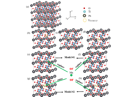
The cubic phase of PT (space group Pm3m), which is often used in the first principles simulations, was chosen as a model to simplify the calculation [22]. For simulations, a supercell [shown in figure 1 (a)] composed of 135 atoms and 27 primitive PT unit cells was established by repeating the unit cell. Then, one vacancy defect (such as VPb, VO and VTi) was introduced into the supercell for the calculation of the native vacancy defect. It is difficult to show the structure of defects in PT with the dense ion arrangement. Thus, supercells were used to illustrate the structure of defects in PT in figures 1 (b) to (h). Additionally, the model structures of Mn defects in PT were built by adding one Mn ion into two kinds of host supercells, one perfect supercell of PT [marked with model #1 in figures 1 (e) and 1 (f)] and the other containing one vacancy defect [marked with model #2 in figures 1 (g) and 1 (h) where VPb was taken as an example]. The concentrations of native defects and Mn defects are all 3.7% in the calculation, while it is about 3% for Mn doping in the experiment [16].
2.2 Computational methods
2.2.1 First-principles
All the total energy calculations were performed in VASP code using the projector-augmented wave (PAW) method [23, 24]. Generalized gradient approximations (GGA) were used in the form of Perdew-Burke-Ernzerhof (PBE) exchange-correlation function for the electron-electron interaction [25]. A Monkhorst-Pack mesh and a plane-wave cutoff energy were determined at and 500 eV, respectively, through calculating the total energy. The convergence of the electronic self-consistent energy less than eV and the force on each atom less than 0.01 eV/Å were defined for full relaxation of the positions of all atoms.
The optimized lattice constant of PT is 3.972 Å, which is very close to the experimental value of 3.97 Å [22]. The band gap of PT was calculated to be 2.40 eV in this paper, which is lower than the experimental value of 3.40 eV [26]. The band gap is always undervalued with the first-principles [27, 28], so the experimental value of 3.40 eV was used in calculation presented below.
2.2.2 Defect formation energies
| (2.1) |
where and are the total energy of the supercell with and without defect, respectively, is the number of atoms which are removed from (or added to) the supercell corresponding to plus (or minus) sign, is its chemical potential, is the charge state of the defect, is Fermi-energy which is calibrated to 0 at the top of the valence band . Finally, a correction term is added to align the reference potential in the defect supercell with that in the bulk.
When the defect formation energies and in two charge states of and are equal, the defect transition Fermi-energy , which is defined as the thermodynamic transition level [29], can be determined as the following form according to equation (2.1):
| (2.2) |
To grow the crystal of PbTiO3 in thermodynamic equilibrium conditions, , , and (the chemical potentials of Pb, Ti, O and PbTiO3) must be satisfied as follows:
| (2.3) |
PbO2, PbO and TiO2 are considered to be major competing phases. The following conditions need to be further taken into account in order to inhibit the undesired phases in PbTiO3 [31]
| (2.4) |
where , and are the chemical potentials of corresponding competing phases. Their corresponding bulk energies of per formula unit are listed in table 1.
| System | (eV) |
|---|---|
| PbTiO3 | |
| TiO2 | |
| PbO | |
| PbO2 |
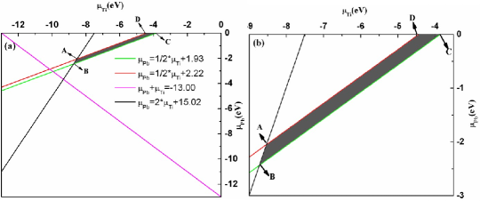
The chemical potentials of Pb, Ti and O, , and , could be determined from equations (2.3) and (2.4) for stable PbTiO3 growth, which were shown on the - plane in figure 2 with a shaded region. Then, the chemical potentials at four vertices (labeled with A, B, C, and D in figure 2, respectively) of the quadrilateral shadow region, listed in table 2, were selected to analyze the defect formation energies, which correspond to four different growth conditions of stable PT growth. A and B points represent the oxygen-rich growth of PT, where is higher, while C and D points are oxygen-poor, which correspond to in table 2. However, they are just opposite for Ti and Pb. Since the amount of Mn doping was very small, the change of chemical potential of Mn was neglected and the energy eV of Mn atom in their bulk crystal phase was used in the calculation. For simplicity, and were used to represent the defects of Mn ions in valence state entering the Pb site and Ti site, respectively, in this paper.
| Chemical potential | (eV) | (eV) | (eV) |
|---|---|---|---|
| A | |||
| B | |||
| C | 0 | ||
| D | 0 |
3 Results and discussion
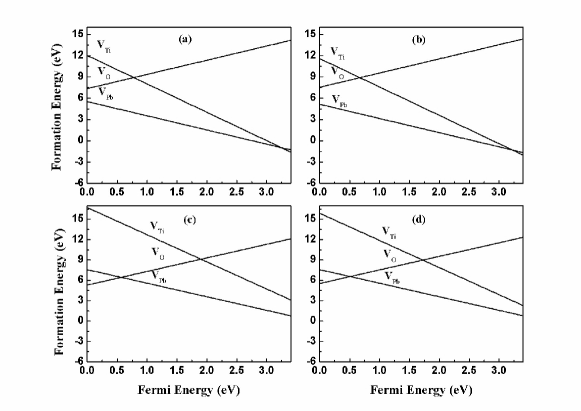
3.1 Analysis of native vacancy defects
The dependence of the formation energies on for native vacancy defects was shown in figure 3 in four different growth conditions which were illustrated with A, B, C and D in figure 2. These results were obtained from the first-principles calculations according to equation (2.1) and the slope of the line represents the charge state of the native vacancy defect. There is a little difference between figures 3 (a) to (d) which can be attributed to the chemical potentials of Pb, Ti and O in four growth conditions. It could be seen that the vacancy formation energy for Pb is generally lower than those for others at all growth conditions as shown in figure 3. It could be concluded that V’s, usually caused by Pb volatilization, are most likely to be formed during the growth process of PT. Our results are consistent with the conclusion drawn in the experiment [20].
3.2 Analysis of Mn defects
3.2.1 Energies
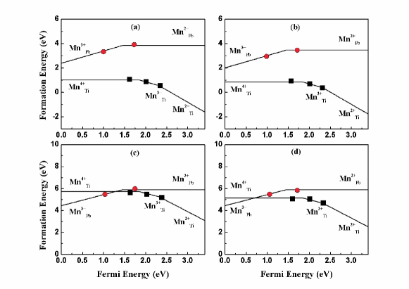
Since VPb is the most probable vacancy defect during the growth process of PT, usually it is possible that a few V’s still exist in PT though the excess Pb is added during preparation process of PT. Thus, Mn defects in PT should be studied based on the Pb vacancy defects. In order to study the effect of VPb on Mn doping in the PT crystal, one Mn impurity is added into Pb site and Ti site in the two kinds of host supercells, respectively. The perfect supercells were marked with model #1 and those with one VPb were marked with model #2 as shown in figures 1 (e) to (h).
In model #1, VPb is not considered in Mn doped PT. The formation energies of Mn defects in different valence states and sites were investigated and discussed in this case firstly. Figure 4 shows the formation energy as a function of for Mn in different configurations with four different growth conditions. The line segments of a different slope were displayed corresponding to different charge states and they connect each other at the corresponding transition level for the same doping defect. The corresponding transition levels are listed in table 3. The formation energies increase with and decreasing of Mn ion’s valence for MnPb, while those are contrary for MnTi. Furthermore, the neutral charge states have obviously higher energies than other charge states for both MnPb and MnTi. It indicated that Mn ion doping into Pb site at a higher valence is more stable, while it is more stable for MnTi at a lower valence, only considering the defect formation energies. It is also noted that the formation energies of MnTi are always much lower than those of MnPb in figures 4 (a) and 4 (b) corresponding to the oxygen-rich growth, while they increase and get close to each other in figures 4 (c) and 4 (d) corresponding to the oxygen-poor growth, which results from the varieties of the chemical potentials of Pb, Ti and O in four growth conditions illustrated in figure 2. The formation energies of still become lower than those of MnPb in this case.
| Mn doped PT without VPb | Mn doped PT with VPb | |||||
|---|---|---|---|---|---|---|
| 1.46 | 1.85 | 2.32 | 1.46 | 0.98 | 1.05 | |
In another case (as described in model #2), VPb is considered in the study of Mn doped PT. When a Mn ion enters the A site, it could compensate VPb, while if it enters the B site, the VPb will be left. The formation energies for Mn in different configurations are analyzed as a function of Fermi energy, and are shown in figure 5. Comparing the formation energies of model #1 (not containing VPb) in figure 4, it can be found that those of MnTi have an increase corresponding to the same growth conditions which results in the formation energies of MnPb that are obviously lower than those of MnTi in figures 5 (c) and 5 (d), while they get close to each other in figures 5 (a) and 5 (b).

The defect formation energies were calculated at corresponding Fermi levels for Mn in different configurations, and listed in table 4 with Fermi levels and the values in [32] too. Their positions are marked with red solid circles for MnPb and with black solid squares for MnTi, respectively, in figures 4 and 5, except that for Mn due to too short line segment in figure 5, which agree with the line segment of their charge state in the diagrams. Since the defect formation energies have a close relationship with the chemical potential selecting, the values in this paper are slightly different from those in the [32]. The stable charge state is the one which has the lowest formation energy for a given Fermi level [29]. The neutral charge states have obviously higher energies than other charge states, and the formation energies of Mn are the lowest in model #1 (not containing VPb), while those of Mn are the lowest in model #2 (containing VPb). Thus, considering minimization of the defect formation energy, it could be concluded that (1) the neutral Mn defects are more unstable than those of other charge states [33]; (2) Mn ions prefer the B sites in +2 valence state in PT without VPb, while Mn ions prefer A sites in +3 valence state in PT with VPb, which shows that A sites are more favored by Mn ions when Pb is deficient.
| Defect | ||||||||
|---|---|---|---|---|---|---|---|---|
| 1.704 | 3.850 | 3.470 | 5.900 | 5.900 | 2.3 | 4.6 | 4.6 | |
| 1.095 | 3.485 | 3.105 | 5.535 | 5.535 | – | – | – | |
| 2.298 | 0.594 | 0.424 | 5.294 | 4.714 | – | – | – | |
| 1.996 | 0.874 | 0.704 | 5.574 | 4.994 | – | – | – | |
| 1.594 | 1.020 | 0.850 | 5.720 | 5.140 | 0.5 | 0.1 | ||
| with VPb | 1.472 | 4.336 | 3.786 | 11.086 | 10.506 | – | – | – |
| with VPb | 1.206 | 5.024 | 4.474 | 11.774 | 11.194 | – | – | – |
| with VPb | 1.009 | 5.250 | 4.700 | 12.00 | 11.420 | – | – | – |
Considering the change of defect configurations in PT with the concentration of Mn doping, based on the conclusion from model #2 (containing VPb), a few Pb deficiencies caused by Pb volatilization in PT could be relieved due to the compensation of Mn ions entering the Pb sites in +3 valence state, which results in a decrease of the trapping electronic charge and makes the domain wall motion easier, thus improving ferroelectric and piezoelectric properties of PT [14, 16]. Then, at a further increase of Mn doping concentration, there will be no V’s needing Mn ions to fill, based on the conclusion from model #1 without VPb, more Mn ions in +2 valence state are more likely to replace Ti4+ to increase oxygen vacancy concentration in PT which results in a decrease of the relative permittivity and loss tangent usually [14, 15, 16, 17, 18]. The measurement of Electron Spin Resonance also shows that Mn ions coexist mainly in the way of Mn2+ and Mn3+ in PZT ceramics [14].
3.2.2 Structure
The volumes of PT supercells with different defects are listed with their change rate compared to that of pure PT in table 5. The supercell has a larger volume change for Mn doping at A site than that for Mn doping at B site at the same valence state, which was also observed in the experimental result of 0.5% Mn doped PZT [16]. Additionally, it becomes larger and larger with Mn ion’s valence. The ionic radii of Pb2+ and Ti4+ are 1.32 Å, 0.64 Å, while those of Mn2+, Mn3+ and Mn4+ are 0.91 Å, 0.65 Å and 0.53 Å, respectively [34]. Consequently, Mn substituting for Pb could produce a large lattice distortion while its substitution for Ti4+ causes a small lattice distortion due to a similar ionic radius between Mn and Ti ions. Greater lattice deformation would lead to the structural change or unstable state of PT eventually by more Mn entering the A site which is not actually found in the experiment. Therefore, it is inferred that Mn ion may enter the A site only at a low concentration while it mainly enters the B site at a high concentration.
| Configuration | Volume (Å) | Change rate |
|---|---|---|
| PT | 1689.41 | – |
| PT with | 1676.33 | % |
| PT with | 1668.77 | % |
| PT with | 1694.70 | 0.31% |
| PT with | 1684.88 | % |
| PT with | 1676.41 | % |
| PT with and VPb | 1688.36 | % |
| PT with and VPb | 1680.00 | % |
| PT with and VPb | 1671.67 | % |
3.2.3 Bader charge
| Atoms | undoping | () | () | () | () |
|---|---|---|---|---|---|
| Pb | 1.35644 | 1.340324 () | 1.34888 () | 1.334463 () | 1.341407 () |
| Ti | 1.846502 | 1.856993 (0.010491) | 1.859499 (0.012997) | 1.840132 () | 1.848042 (0.00154) |
| O | (0.002667) | (0.010304) | () | () |
| Defect | |||
|---|---|---|---|
| 7.00 | 5.723836 | 1.276164 | |
| 7.00 | 5.632596 | 1.367404 | |
| 7.00 | 5.484108 | 1.515892 | |
| 7.00 | 5.431728 | 1.568272 | |
| 7.00 | 5.374644 | 1.625356 |
Average Bader charges of Pb, Ti and O of PT with and without Mn doping at different sites are listed in table 6, respectively. One Ti ion and one Pb ion correspond to three O ions according to stoichiometric ratio in PT and the increase of positive charge of Ti and Pb ions always corresponds to the increase of negative charge of O ions which could be verified by average Bader charges of Pb, Ti and O (). The charge number of O ion is reduced for Mn entering the A-site compared with undoped PT which indicates that the electronegativity of O becomes weaker. The electronegativity of O could affect the binding force between ions. Thus, when Mn enters the A site, the binding force between ions becomes weaker, which makes the domain movement easier in PT to improve the electromechanical performance of PT, while Mn entering the B site is the opposite.
The bonding mode of Mn ion entering the different position of PT directly affects the charge distribution of PT which results in the change of its performance. The Bader charges of Mn ions at different lattice sites are listed in table 7, respectively. Mn ions lost more electrons entering the B site than entering the A site, which shows that the ionicity of the chemical bond is stronger when Mn ion enters the B site. In addition, the ionicity of Mn increases with its valence.
4 Conclusion
Mn defects in PT have been studied by the first-principles based on the native vacancy defects. The defects of MnPb and MnTi were analyzed in two different lattice models with and without Vs which are the most probable vacancy defects to occur during the growth process of PT. It is found that whether Mn ion enters A or B site of PT is related to its doping concentration. PT prefers to incorporate Mn on Pb sites rather than Ti sites with the Pb deficiencies at a low Mn concentration, while a B-site Mn doping is preferable at a high concentration. Mn ion entering the A site with valence could result in the lattice distortion of PT becoming larger and the electronegativity of O becoming weaker, which makes the domain movement easier in PT to improve the performance of PT.
Acknowledgements
The work was supported by the National Natural Science Foundation of China (No. 11705136), the Special Foundation of Shaanxi Educational Commission (No. 17JK0435), the Natural Science Foundations of Shaanxi Province of China (No. 2018JQ1048 and No. 2020JQ-656).
References
- [1] Niu X. S., Jia W., Qian S., Zhu J., Zhang J., Hou X. J., Mu J. L., Geng W. P., Cho J. D., He J., Chou X. J., ACS Sustainable Chem. Eng., 2019, 7, 979–985, doi:10.1021/acssuschemeng.8b04627.
- [2] Engholm M., Bouzari H., Christiansen T. L., Beers C., Bagge J. P., Moesner L. N., Diederichsen S. E., Stuart M. B., Jensen J. A., Thomsen E. V., Sens. Actuators, A, 2018, 273, 121–133, doi:10.1016/j.sna.2018.02.031.
-
[3]
Kudela P., Radzienski M., Ostachowicz W., Yang Z. B., Mech. Syst. Sig. Process., 2018, 108, 21–32,
doi:10.1016/j.ymssp.2018.02.008. - [4] Wang H., Chen Z. F., Xie H. K., Sens. Actuators, A, 2020, 3091, 112018, doi:10.1016/j.sna.2020.112018.
- [5] Li J. F., Zhu Z. X., Lai F. P., J. Phys. Chem. C, 2010, 114, 17796–17801, doi:10.1021/jp106384e.
- [6] Wongdamnern N., Triamnak N., Ngamjarurojana A., Laosiritaworn Y., Ananta S., Yimnirun R., Ceram. Int., 2008, 34, 731–734, doi:10.1016/j.ceramint.2007.09.048.
- [7] Tong S., Ma B. H., Narayanan M., Liu S., Koritala R., Balachandran U., Shi D., ACS Appl. Mater. Interfaces, 2013, 5, 1474–1480, doi:10.1021/am302985u.
- [8] Hu G. L., Ma C. R., Wei W., Sun Z. X., Lu L., Mi S. B., Liu M., Ma B. H., Judy W., Jia C. L., Appl. Phys. Lett., 2016, 109, 193904, doi:10.1063/1.4967223.
-
[9]
Mahato D. K., Molak A., Szeremeta A. Z., Mater. Today: Proc.,
2017, 4, 5488–5496,
doi:10.1016/j.matpr.2017.06.004. -
[10]
Wang Z., Ren W., Ren J. B., Wu X., Shi P., Chen X., Yao X., Ferroelectrics, 2009, 383, 151–158,
doi:10.1080/00150190902889333. -
[11]
Kozielski L., Adamczyk M., Erhart J., Pawełczyk M., J.
Electroceram., 2012, 29, 133–138,
doi:10.1007/s10832-012-9746-z. - [12] Zhang M. F., Wang Y., Wang K. F., Zhu J. S., Liu J. M., J. Appl. Phys., 2009, 105, 061639, doi:10.1063/1.3055338.
- [13] Feigl L., Pippel E., Pintilie L., Alexe M., Hesse D., J. Appl. Phys., 2009, 105, 126103, doi:10.1063/1.3141733.
- [14] He L. X., Li C. E., J. Mater. Sci., 2000, 35, 2477–2480, doi:10.1023/A:1004717702149.
- [15] Liu Y. B., Xu Z., Li Z. R., Zhuang Y. Y., Tian Y., Hu D., Song K. X., Guo H. S., J. Alloys Compd., 2018, 742, 958–965, doi:10.1016/j.jallcom.2018.01.027.
- [16] Xin H., Ren W., Wu X. Q., Shi P., J. Appl. Phys., 2013, 114, 027017, doi:10.1063/1.4812226.
- [17] Hennings D., Pomolun H., J. Am. Ceram. Soc., 1974, 57, 527–532, doi:10.1111/j.1151-2916.1974.tb10802.x.
-
[18]
Yu Y., Wu J. G., Zhao T. L., Dong S. X., Gu H. S., Hu Y. M., J. Alloys Compd., 2014,
615, 676–682,
doi:10.1016/j.jallcom.2014.06.144. -
[19]
Limpijumnong S., Rujirawat S., Boonchun A., Smith M. F., Cherdhirunkorn B.,
Appl. Phys. Lett., 2007,
90, 103113, doi:10.1063/1.2711200. -
[20]
Wang L., Yu J., Wang Y., Gao J., J. Mater. Sci.: Mater. Electron., 2008, 19, 1191–1196,
doi:10.1007/s10854-007-9524-x. -
[21]
Dimos D., Schwartz R. W., Lockwood S. J., J. Am. Ceram. Soc.,
1994, 77, 3000–3005,
doi:10.1111/j.1151-2916.1994.tb04536.x. - [22] Wang J. L., Tang G., Wu X. S., Pu L., J. Mater. Sci., 2014, 49, 4715–4721, doi:10.1007/s10853-014-8171-x.
- [23] Kresse G., Joubert D., Phys. Rev. B, 1999, 59, 1758, doi:10.1103/PhysRevB.59.1758.
- [24] Kresse G., Furthmüller J., Phys. Rev. B, 1996, 54, 11169, doi:10.1103/PhysRevB.54.11169.
- [25] Perdew J. P., Burke K., Ernzerhof M., Phys. Rev. Lett., 1996, 78, 1396, doi:10.1103/PhysRevLett.78.1396.
- [26] Robertson J., Warren W. L., Tuttle B. A., J. Appl. Phys., 1995, 77, 3975–3980, doi:10.1063/1.358580.
-
[27]
Xiao P., Fan X. L., Liu L. M., Lau W. M., Phys. Chem. Chem. Phys., 2014,
16, 24466–24472,
doi:10.1039/c4cp03453h. -
[28]
Fang Y. Z., Kong X. J., Wang D. T., Cui S. X., Liu J. H., Chin. J. Phys.,
2018, 56, 1370–1377,
doi:10.1016/j.cjph.2018.04.011. - [29] Van de Walle C. G., Neugebauer J., J. Appl. Phys., 2004, 95, 3851–3879, doi:10.1063/1.1682673.
-
[30]
Kubota T., Nakamura A., Toyoura K., Matsunaga K., Acta
Biomater., 2014, 10, 3716–3722,
doi:10.1016/j.actbio.2014.05.007. -
[31]
Buckeridge J., Scanlon D. O., Walsh A., Catlow C. R. A., Comput.
Phys. Commun., 2014, 185, 330–338,
doi:10.1016/j.cpc.2013.08.026. -
[32]
Boonchun A., Smith M. F., Cherdhirunkorn B., Limpijumnong S., J. Appl.
Phys., 2007, 101, 043521,
doi:10.1063/1.2654120. - [33] Hayashi K., Ando A., Hamaji Y., Sakabe Y., Jpn. J. Appl. Phys. Part 1, 1998, 37, 5237, doi:10.1143/JJAP.37.5237.
-
[34]
Shannon R. D., Acta Crystallogr., Sect. A: Found. Crystallogr., 1976, A32, 751–767,
doi:10.1107/S0567739476001551.
Ukrainian \adddialect\l@ukrainian0 \l@ukrainian
Öåíòðè ëåãóâàííÿ i âàëåíòíiñòü iîíiâ Mn ó PbTiO3 íà îñíîâi ïðèðîäíèõ äåôåêòiâ âàêàíñié Ã. Ñií, Ê. Ïàíã, Ä.Ë. Ãàî, Ë. Ëi, Ï. Æàíã
Íàóêîâèé êîëåäæ óíiâåðñèòåòó àðõiòåêòóðè i òåõíîëîãié ì. Êñÿí, Êñÿí, 710055, ÊÍÐ