Dynamic quarter-wave metasurface for efficient helicity inversion of polarization beyond the single-layer conversion limit
Abstract
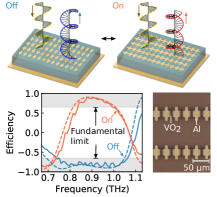
Terahertz chiral sensing and polarization-multiplexing communication demand subwavelength devices that dynamically invert polarization helicity. Metasurfaces can enhance anisotropy and fine tunability at subwavelength scales for this purpose. Although metasurfaces enabling deep modulation between orthogonal polarizations have been designed, they suffer from low conversion efficiencies. In this study, it is shown that the efficiency of conversion from linear to circular polarization by conventional single-layer transmissive metasurfaces cannot exceed a fundamental limit. A dynamic reflective metasurface free from this limitation is then proposed. The device includes multilayer structures working as a terahertz quarter-wave plate with switchable slow and fast axes. A phase transition of vanadium dioxide induces the necessary structural transformation of the metallic patterns. A practical fabrication method, based on the room-temperature bonding technique of sapphires, is presented. Dynamic helicity inversion is demonstrated at , with a conversion efficiency of over 80 % that is beyond the fundamental limit of single-layer transmissive metasurfaces () and more than four times greater than that of previously reported devices.
Mitsuki Kobachi Fumiaki Miyamaru Toshihiro Nakanishi Kunio Okimura Atsushi Sanada
Yosuke Nakata*
M. Kobachi, Prof. A. Sanada
Graduate School of Engineering Science, Osaka University, Osaka 560-8531, Japan
Prof. F. Miyamaru
Department of Physics, Faculty of Science, Shinshu University, Nagano 390-8621, Japan
Dr. T. Nakanishi
Department of Electronic Science and Engineering, Kyoto University, Kyoto 615-8510, Japan
Prof. K. Okimura
School of Engineering, Tokai University, Kanagawa 259-1292, Japan
Dr. Y. Nakata
Graduate School of Engineering Science, Osaka University, Osaka 560-8531, Japan
Center for Quantum Information and Quantum Biology, Osaka University, Osaka 560-8531, Japan
Email Address: nakata@ee.es.osaka-u.ac.jp
Keywords: Metasurfaces, Metamaterials, Polarization, Helicity, Vanadium dioxide, Terahertz devices
1 Introduction
Polarization is one of the most fundamental properties of electromagnetic waves. It plays a crucial role in applications such as liquid-crystal displays, polarization-sensitive spectroscopy, and polarization-multiplexing communication. As polarization control demands an anisotropic response, birefringent materials have been widely employed in static polarization devices, such as polarizers and wave plates. However, the anisotropy of natural materials is typically small and limited to fixed values. Polarization devices based on birefringent materials involve a thickness much larger than the working wavelength. Therefore, they become bulky, especially in the lower frequency (e.g., microwave and terahertz) range.
Artificial structural surfaces called metasurfaces can be leveraged to enhance anisotropy and make devices compact [1, 2]. They can exhibit a considerable anisotropic response even at subwavelength thicknesses, when metal or dielectric resonators are introduced. As this response originates in anisotropic structural resonances, it can be finely tuned by appropriate design of the structures on the metasurface. Thus, metasurfaces can provide both larger anisotropy and wider tunability for polarization control than can natural materials, the characteristics of which are determined by the atomic constituents. A variety of static-polarization-control metasurfaces have been developed in the microwave-to-optical frequency range, including static metasurface polarizers [3, 4] and wave plates [5, 6, 7, 8, 9, 10]. However, for sensitive measurement and communication technologies, dynamic modulation of polarization is an essential requirement. Therefore, considerable effort has been devoted to developing metasurface modulators [11, 12]. In the microwave region, varactor diodes have been used to realize tunable phase shifts [13] and dynamic polarization rotations of arbitrarily polarized incident waves [14]. A power-dependent metasurface switchable between a quarter-wave plate and a spatial wave manipulator has also been proposed [15]. Even in the terahertz region, a high-electron-mobility transistor (HEMT) has been used to produce a dynamic phase shift [16]; graphene has also been applied to a gate-tunable THz polarizer [17]. Photoexcitation of semiconductors could enable ultrafast terahertz polarization modulation using gratings [18, 19] and chiral structures [20, 21, 22].
For continuous polarization tuning, micro-electro-mechanical systems (MEMS) have been applied to polarization modulators with chiral structures [23, 24]; polarization converters with tunable cross-conversion rates [25]; tunable wave plates that can modulate a transmitted wave from pure circular to linear polarization [26]; and kirigami polarization modulators [27]. Phase-changeable materials provide another approach to polarization control, advantageous for deep modulation. For example, vanadium dioxide has been employed in metasurfaces [28], because it can induce a high-contrast resistance change over the factor of in phase change [29] that has been used to alter critically the operating frequencies of THz quarter-wave plates [30, 31]. In contrast to simple operating-frequency modulation, polarization modulation at a specific frequency requires more complex designs of structures working for both states before and after the phase transition. Dynamic modulation between linear and circular polarizations has been demonstrated by using I-shape structures [32]. To realize deeper polarization modulation, checkerboard structures have been utilized in switchable linear polarizers with a high extinction ratio [33] and helicity-switchable quarter-wave plates that achieve orthogonal-polarization modulation [34, 35]. However, these vanadium-dioxide polarization devices, based on single-layer designs, suffer from a low conversion efficiency for incident waves, attributable to reflection loss from both substrate and metasurface. Substrate Fresnel reflection could be reduced by using an extremely thin substrate (although implementing this is challenging), but reflection loss from the metasurface is unavoidable even in principle [6]. These two factors prevent the simultaneous achievement of orthogonal-polarization modulation and high efficiency, especially in terahertz or higher frequency regions. Although multilayer vanadium-dioxide metasurfaces have been seen as promising for use in efficient multifunctional devices, such as reconfigurable absorbers [36, 37, 38, 39, 40, 41, 42, 43, 44, 45, 46, 47, 48], reprogrammable wavefront-engineering metasurfaces [49, 50], and devices switchable between quarter- and half-wave plates [51], these proposals have not been realized experimentally, because of the stringent fabrication challenges. Although a few studies have reported experimental realization of multilayer vanadium-dioxide structures for infrared polarization modulation [52] and terahertz asymmetric transmission [53], they did not focus on orthogonal-polarization modulation.
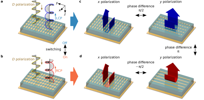
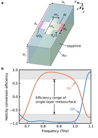
In this study, we experimentally demonstrate dynamic helicity inversion with high conversion efficiency in the terahertz region necessary for chiral sensing and communication technologies. As mentioned above, transmissive metasurfaces are known empirically to suffer from low conversion efficiencies. We begin by deriving a theoretical limit for the conversion efficiency of single-layer transmissive metasurfaces between linear and circular polarization. We then propose a dynamic reflective metasurface with transformable metallic structures capable of overcoming this limitation. As shown in Figure 1a and b, the device efficiently converts a linearly polarized wave into a reflected circularly polarized one with switchable helicity. The device works as a dynamic quarter-wave plate with exchangeable slow and fast axes. The structure is designed to achieve orthogonal-polarization modulation from the incident linearly polarized radiation with high conversion efficiency. To resolve the fabrication challenges of multilayer structures, we developed a fabrication method based on sapphire room-temperature bonding techniques [54] that is compatible with the vanadium-dioxide process. Finally, we realize the proposed device physically and demonstrate its highly efficient helicity-switching function in the terahertz frequency range. Note that we use the convention of a harmonic time dependence with imaginary unit in this study.
2 Results and Discussion
2.1 Helicity conversion efficiency limit of single-layer metasurfaces
First, we define a figure of merit for helicity conversion using quarter-wave plates. Consider a plane wave propagating in the direction and normally incident on a quarter-wave plate with fast and slow axes along the and axes (or vice versa). As the quarter-wave plate can convert diagonal () linear polarization ( polarization) into a circular one, we assume that the incident wave has polarization . In a previous paper [34], the component of the Stokes parameter was divided by the transmitted power flux to define a circular-polarization ratio
| (1) |
where () is the complex amplitude transmittance of the polarization. Equation (1), which characterizes the purity of the output helicity state converted from -polarization, can be used to evaluate the polarization-state modulation rate. Here, corresponds respectively to a pure right- or left-circularly polarized wave when viewed from the receiver. We next introduce the helicity-conversion efficiency
| (2) |
where is the incident-beam power flux. represents a perfect dissipation-free conversion from linear polarization to right- or left-circular polarization, respectively. We can use as a figure of merit that includes both polarization and efficiency information.
Next, we derive the fundamental maximum limit of for single-layer transmissive metasurfaces. In contrast to the avoidable substrate Fresnel loss, metasurface reflection loss is inevitable. Consider a plane wave normally incident on a transmissive electric metasurface at in a vacuum. The metasurface has an infinitesimally small thickness in the long-wavelength approximation, where the Fresnel reflection of the substrate is negligibly small. For simplicity, we assume that the incident frequency is lower than the diffraction frequency, and the metasurface has mirror symmetry with respect to either or . Then, there is no diffraction into higher-order modes and no cross conversion between and polarizations: the metasurface behaves as a sheet characterized by different complex-amplitude transmittances and . From the boundary conditions of electric-field continuity and energy conservation, the complex transmittance must satisfy the constraint
| (3) |
i.e., the transmittance is constrained at the circumference of a circle with 1/2 center and 1/2 radius in the complex plane. High transmission only occurs when ; a large transmission phase leads to transmission deterioration. From this restriction, the helicity-conversion efficiency has its maximum of for and . Thus, single-layer transmissive metasurfaces have a fundamental efficiency limitation even if we eliminate substrate reflection.
2.2 Design principles of multi-layered device
To overcome the limitation described above, we propose a reflective metasurface on a dielectric substrate with a metal ground. In contrast to transmissive devices, a reflective device does not have unwanted scattering channels that cause dissipation. Thus, a reflective metasurface allows perfect polarization conversion in an ideal case without the fundamental limitation of single-layer transmissive devices and with much higher efficiency. Note that single-layer reflective converters with prisms have already enabled non-orthogonal modulation between linear and circular polarization, but they are bulky and exhibit prism reflection [55]. Thus, we should consider a multilayer reflective device.
To implement the necessary structural transformation, we utilize vanadium dioxide, which exhibits a metal–insulator transition at a critical temperature of [56]. The transition involves change of vanadium-dioxide crystalline structures, but the resistivity variation is stable under multiple cycles of transitions [57]. When the device is off, it is in its low-temperature (insulating) state; it is in its high-temperature (metallic) state when on. To convert polarization into circular polarization, a phase shift between the and polarizations is necessary. When we assume mirror symmetry, the device independently responds to and polarizations, which may therefore be treated separately. First, we consider an off-state device, as shown in Figure 1c. Because the metallic patches are shorter than the target wavelength, most of the incident - and -polarized waves are transmitted through the dielectric surface and reflected back at the ground plane. To induce a phase shift between polarizations, the lengths of the metallic structures are tuned. Second, we consider the on-state device [Figure 1d]. The temperature change induces a structural deformation along the axis from metal patches to the wire grid. The -polarized wave of wavelength is now reflected at the surface due to the wire-grid response [3]. The thickness of the dielectric substrate is set to approximately ; this induces a round-trip phase shift of radians between the off and on states. Combining the structures in the and directions, we can realize helicity switching, as shown in Figure 1a and b. When a normally incident wave with () polarization enters the off-state device, the phase difference between the and polarizations converts the polarization into left-circular polarization. When the device is turned on, the additional -radian phase shift is added only to the polarization, leading to helicity inversion of the reflected wave.
2.3 Simulation
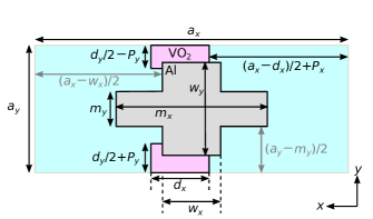
To design the device structures, we use an electromagnetic-field simulator COMSOL Multiphysics. Figure 2a shows the device unit cell. Exploiting of the mirror symmetries, we reduced computational costs by performing the calculation only for a quarter part of the unit cell with appropriate boundary conditions. The device is placed in vacuum and has a sapphire dielectric substrate; its refractive indices are and [58]. The sapphire orientation is chosen so that the c plane lies on the surface, where the vanadium dioxide grows finely because of lattice matching [56]. On the bottom of the sapphire substrate, we place a gold ground plane, which is represented in the simulation by an impedance boundary with an effectively infinite thickness. Aluminum and vanadium-dioxide patterns are formed on the top of the c-plane substrate. The aluminum region is treated as a transition boundary with a thickness of . The conductivities of gold and aluminum are and , respectively [59]. The vanadium dioxide is represented by a sheet resistance of and for the off and on states, respectively. The - and -polarized waves impinge on the surface normally, and complex reflection amplitudes are calculated. We set the substrate thickness to to induce a phase difference between the off and on states for a -polarized wave at . Next, we consider the structures, described by the dimensional parameters defined in Figure 2a. After setting , we specify , , , and , and confirm an approximately phase difference between on and off states for polarization. After this, we consider an incidence of an -polarized wave, and adjust and to produce a phase difference between - and -polarized waves for the off state. The parameters are chosen so that the helicity conversion efficiency is as high and the working bandwidth as broad as possible, while keeping feasible : they are determined to be , , , , , , and .
Figure 2b shows the calculated helicity-conversion efficiency , along with the efficiency limit of a single-layer transmissive metasurface. (Note that the propagation-direction change in reflection demands the minus sign, in contrast to Equation (2).) At a frequency of , helicity conversion efficiency reaches and for the off and on states, respectively. The degradation from perfect efficiency is caused by Ohmic and dielectric loss. Nevertheless, the efficiencies of both off and on states significantly exceed the theoretical efficiency limit () of the single-layer transmissive metasurface. Detailed simulation results on the helicity conversion efficiency and circular-polarization ratio for the intermediate state of vanadium dioxide are presented in Supplementary Information.
2.4 Physical device
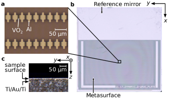
The proposed metasurface design poses a fabrication challenge because it involves multiple layers. We prepared a thin sapphire plate with a metal ground by room-temperature bonding with thin metal films [54]. Because room-temperature bonding is free from glue, it is tolerant of the high temperatures and chemical treatments required in the vanadium dioxide process. The vanadium dioxide and aluminum patterns on the substrate were fabricated by a conventional photolithography technique [34, 35]. Detailed information about the process is provided in the Experimental Section.
Figure 3a and b show photomicrographs of the metasurface and a picture of the entire fabricated device, respectively. Although there was an unintended shift of the vanadium-dioxide structures relative to the aluminum ones, they connected with each other well. The structural parameters measured for the actual sample are provided in the Experimental Section. Figure 3c offers a side view of the sample. The sapphire plates were well-attached by the room-temperature bonding technique, and the bonding was not broken after high-temperature treatment and chemical etching.
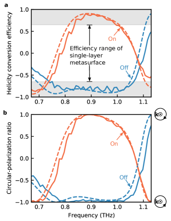
To demonstrate the performance of the device, we conducted conventional terahertz time-domain spectroscopy. Detailed information about this experiment is provided in the Experimental Section. For comparison, we recalculate the device’s performance using the measured parameter values from the Experimental Section. Figure 4a compares the helicity-conversion efficiency in the experiment and the realistic simulation. The experimental data agree well with the simulated ones. At , the experimental helicity-conversion efficiency reaches and for the off and on states, respectively. These are both far beyond , the theoretical efficiency limit of single-layer transmissive metasurfaces. To evaluate the improvement quantitatively, we compare the conversion efficiency with that of previous transmissive devices [34, 35]. The helicity-conversion efficiency of the dipole-nested-checkerboard metasurface is and at [34], while that of the deformed-checkerboard metasurface is and at [35]. These efficiencies are much lower than the theoretical conversion efficiency of , because of the multiple reflections inside the substrates, and the efficiencies are evaluated for the first transmitted pulse. The efficiency of the proposed device is more than four times higher, because it does not suffer from the scattering loss from the substrate and metasurface. Other reported devices do not achieve orthogonal modulation, and their transmission efficiencies are similar to the above checkerboard devices because of substrate reflections [26, 30, 31, 32].
We also evaluated the circular-polarization ratio to determine the purity of the output polarization. Figure 4b shows experimental and simulated . The experimental circular-polarization ratio at is for the off state and for the on state. These data indicate that each reflected wave is in a state close to pure circular polarization. Thus, our device is not only highly efficient, but also achieves deep modulation between orthogonal circular polarizations.
2.5 Discussion
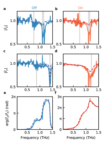
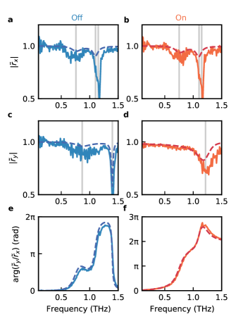
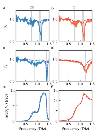
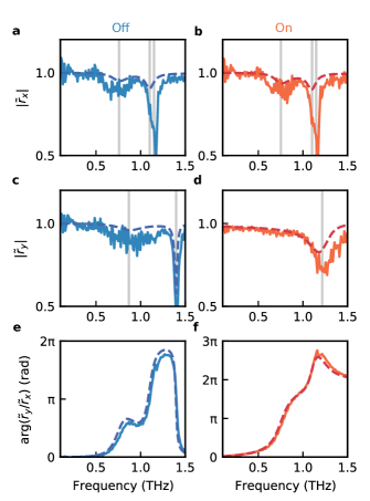
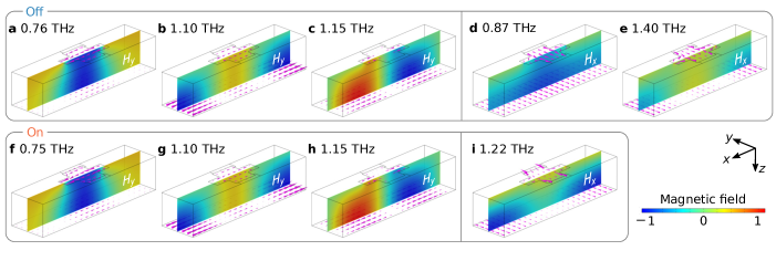
To show the details of the device operation, we summarize the reflection amplitudes and and the phase difference in Figure 5. The solid lines represent the measured data, and the dashed lines represent the simulated data; the agreement of the two is generally good. The data confirm remarkably high reflectivity, which leads to a high device efficiency up to . The phase shift between and polarizations is realized at . Interestingly, the phase difference of the off state showed a plateau around , which indicates that the phase rotations of and with increasing cancelled out. However, such a phase plateau was not observed for the on state. If an on-state plateau could be realized, we could achieve a much broader operation. The dips around can be explained by energy leakage to the waveguide modes. Because the structures act as grating couplers, the incident wave can couple to the waveguide mode. The frequency of the transverse magnetic (TM) waveguide mode with grating wavenumber is theoretically estimated to be [60], assuming that sapphire has an isotropic refractive index of .
The stability of the device is also important for applications. In Supplemental Information, we present the reflection characteristics of the device measured at different cycles of heating and cooling operations on three different days. No performance degradation was observed in the cycles. Moreover, a previous report indicates that hundred cycles of operations do not alter the VO2 characteristics [57].
The underlying physics can be elucidated by an eigenmode analysis of the realistic model without excitation. As impedance and transition boundaries cannot be used in eigenmode analysis, we represent the aluminum and gold regions as perfect electric conductors in this simulation. The calculated eigenfrequencies are depicted as gray lines in Figure 5. The corresponding eigenmodes, depicted in Figure 6, induce phase rotations around the resonant frequencies. Eigenmodes with current flowing along the and axes are termed - and -polarized modes, respectively. For the off state, the -polarized mode at [Figure 6a] and the -polarized mode at [Figure 6d] maintain around the working frequency of . The -polarized modes at and in the off state merge into another resonant mode at in the on state. This change causes a -radian phase shift for target polarization. The modes around and are split from the waveguide modes by introducing a periodic structure. As their currents flow in the direction, their frequencies do not shift with switching from off to on. The waveguide modes at have antisymmetric current distributions in the direction. The antisymmetric waveguide mode cannot be excited in the simulation because of the symmetry of the incident plane wave. However, it can be excited experimentally, because of the spatially-nonuniform field distribution of the incident wave. In practice, we used a lens to focus the incident wave, as explained in the Experimental section. This antisymmetric waveguide mode explains the reflection dip at , which was only observed in experiments. The excited waveguide mode propagates inside the sapphire and can emit from the side. This leakage might contribute to the linewidth broadening of the dips around , as shown in Figure 5a and b.
3 Conclusion
In this study, we achieved orthogonal-polarization modulation with high conversion efficiency in terahertz helicity switching by leveraging a dynamic reflective quarter-wave metasurface. The helicity-conversion efficiency reached and at , which is far beyond the efficiency limit for single-layer transmissive metasurfaces (). Our device had more than four times the efficiency of devices in previous studies [34, 35]. In addition, the purity of its output helicity reached and . These results indicate the decisive advantage of using dynamic reflective metasurfaces for orthogonal-polarization modulation.
Compared to PIN-diode approach for a microwave helicity switchable metasurface under circular-polarization illumination [61], vanadium-dioxide devices are free from soldering and allow operation in terahertz frequency range. In addition, our device works as a quarter-wave plate that does not require circular-polarization illumination for helicity switching. Due to the scale invariance of Maxwell’s equations, the proposed design scheme is applicable not only in the terahertz frequency range, but also in other frequency ranges from microwave to infrared regions, using suitable metal, dielectric, or high-contrast conductivity-changeable materials. To reach the higher frequency range, GST (Ge2Sb2Te5) might be a suitable choice of dielectric phase-changeable material [62]. Although the switching speed of our device is limited by the heater response time ( minutes) in our experiments, the potential switching speed of vanadium dioxide is much faster [63]. Ultrafast switching could be realized by photoexcitation of vanadium dioxide [64] or semiconductors [19]. Moreover, broadening of the operating bandwidth of the device is another interesting problem. Checkerboard structures might be helpful for achieving broadband operation [35]. The room-temperature-bonding technique developed here is compatible with high temperature and chemical etching, and is applicable to switchable multifunctional terahertz devices [47, 49, 50].
4 Experimental Section
Substrate Bonding:
Two substrates of c-plane sapphire were prepared and coated with titanium (thickness: ) on their top surfaces as an adhesion layer. A layer of gold thick was deposited on the titanium on one sample, while a gold layer thick was formed on the titanium on the other sample. The extremely flat gold sides of these substrates were bonded by gold diffusion at room temperature: this worked like glue, without introducing other materials. This room-temperature bonding technique is highly compatible with the vanadium-dioxide process, which involves high-temperature and chemical treatment. Next, one side of the sapphire was polished to a thickness of . Finally, the substrate was cut into plates.
Photolithography:
First, we deposited a -thick VO2 film on the bonded sapphire substrate. We used reactive magnetron sputtering with a vanadium target in O2 and Ar flow. During the sputtering, the temperature of the substrate was kept at 600 . Next, we coated the photoresist on the VO2 film and exposed it, using a maskless exposure system. After the development of the photoresist, the VO2 pattern was formed by wet etching in a solution comprising phosphoric acid, nitric acid, acetic acid, and water in the proportions 16:1:2:1. Because the vanadium-dioxide patterns were over-etched, the exposure was intentionally larger than the original design parameter. The aluminum pattern was fabricated by lift-off techniques. Half of the surface had the structures, while the other half was a uniform aluminum sheet used as a reference mirror. By coating, exposing, and developing the photoresist, we left it in place except in the pattern region. Finally, a -thick aluminum pattern was formed by electron-beam evaporation and lift off.
Sample-size characterization:
The size of the fabricated sample was characterized by optical microscopy. The geometric parameters are defined in Figure 7. Their measured values were as follows:
, , , , , , , and . The displacement of the VO2 pattern was evaluated as and . The thickness of the substrate was estimated to be by observing interference fringes of the reflected white light with a spectrometer, assuming the refractive index of sapphire to be 1.76. The direct-current (DC) sheet resistance of the vanadium dioxide was measured as in the off state () and in the on state ().
These parameters were used in the realistic simulation discussed in Figure 4, 5, and 6. When calculating reflection spectra, the boundary conditions used for aluminum and bottom gold were kept unchanged from the design simulation. The aluminum and gold were assumed to be perfect conductors in the eigenmode analysis.
Terahertz Reflection Measurement:
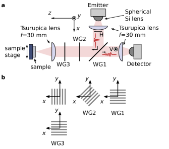
Conventional terahertz time-domain spectroscopy was performed in a reflective setup. Figure 8 shows a schematic picture of the terahertz system. Photoconductive antennas were excited by femtosecond-laser pulses to emit and detect a terahertz pulse in the time domain. Horizontally polarized radiation from the emitter was collimated by a lens and then reflected by the first wire grid (WG1). As the wires of WG1 were parallel to the axis, the incident wave was mostly reflected by them and then passed through grids WG2 and WG3 before reaching the sample. The wires in WG2 were aligned along the diagonal () direction, while those in WG3 were set parallel to the or directions for the or measurements, respectively. Eventually, the wave was focused on the sample by a lens. The full width at half maximum (FWHM) of the beam spot was . Radiation reflected by the sample then partially passed through WG2. Finally, a part of the wave was transmitted through WG1 to the detector. The measurements were taken in a sealed box filled with dry air. First, we measured the temporal reference signal reflected from the aluminum reference mirror on the sample. After translating the sample holder, we obtained the temporal signal reflected from the metasurface. To ensure phase accuracy, the displacement direction of the sample stage was precisely adjusted to be parallel to the sample surface. We took the Fourier transform of the signals and calculated the complex reflection amplitudes . We averaged the reflection-amplitude data obtained by repeating this procedure ten times. The measurement was performed for four sets of , where and metasurface-temperature (off) or (on).
Acknowledgements
The authors would like to thank Hitoe Kon in Adamant Namiki Precision Jewel Co., Ltd. for her technical contribution to sapphire bonding. We are also grateful to Akira Inokuma and Yuma Takano for their helpful comments on the manuscript, and Kei Iyoda and Masayuki Fujita for technical assistance. This study was supported by a grant from the Murata Science Foundation. A part of this work was supported by the Kyoto University Nano Technology Hub in “Nanotechnology Platform Project” sponsored by the Ministry of Education, Culture, Sports, Science and Technology (MEXT), Japan.
References
- [1] H.-T. Chen, A. J. Taylor, N. Yu, Rep. Prog. Phys. 2016, 79, 7 076401.
- [2] Q. He, S. Sun, S. Xiao, L. Zhou, Adv. Opt. Mater. 2018, 6, 19 1800415.
- [3] K. Takano, H. Yokoyama, A. Ichii, I. Morimoto, M. Hangyo, Opt. Lett. 2011, 36, 14 2665.
- [4] T. Suzuki, M. Nagai, Y. Kishi, Opt. Lett. 2016, 41, 2 325.
- [5] N. K. Grady, J. E. Heyes, D. R. Chowdhury, Y. Zeng, M. T. Reiten, A. K. Azad, A. J. Taylor, D. A. R. Dalvit, H.-T. Chen, Science 2013, 340, 6138 1304.
- [6] X. Ding, F. Monticone, K. Zhang, L. Zhang, D. Gao, S. N. Burokur, A. de Lustrac, Q. Wu, C.-W. Qiu, A. Alù, Adv. Mater. 2015, 27, 7 1195.
- [7] Y. Nakata, Y. Taira, T. Nakanishi, F. Miyamaru, Opt. Express 2017, 25, 3 2107.
- [8] Z. Han, S. Ohno, Y. Tokizane, K. Nawata, T. Notake, Y. Takida, H. Minamide, Opt. Lett. 2018, 43, 12 2977.
- [9] W. Liu, T. Yu, Y. Sun, Z. Lai, Q. Liao, T. Wang, L. Yu, H. Chen, Phys. Rev. Appl. 2019, 11, 6 064005.
- [10] X. You, R. T. Ako, W. S. L. Lee, M. Bhaskaran, S. Sriram, C. Fumeaux, W. Withayachumnankul, APL Photonics 2020, 5, 9 096108.
- [11] E. Herrmann, H. Gao, Z. Huang, S. R. Sitaram, K. Ma, X. Wang, J. Appl. Phys. 2020, 128, 14 140903.
- [12] K. Konishi, T. Kan, M. Kuwata-Gonokami, J. Appl. Phys. 2020, 127, 23 230902.
- [13] B. O. Zhu, J. Zhao, Y. Feng, Sci. Rep. 2013, 3, 1 3059.
- [14] Z. Wu, Y. Ra’di, A. Grbic, Phys. Rev. X 2019, 9, 1 011036.
- [15] M. Kiani, A. Momeni, M. Tayarani, C. Ding, Opt. Express 2020, 28, 23 35128.
- [16] Y. Zhang, Y. Zhao, S. Liang, B. Zhang, L. Wang, T. Zhou, W. Kou, F. Lan, H. Zeng, J. Han, Z. Feng, Q. Chen, P. Mazumder, Z. Yang, Nanophotonics 2018, 8, 1 153.
- [17] Z. Miao, Q. Wu, X. Li, Q. He, K. Ding, Z. An, Y. Zhang, L. Zhou, Phys. Rev. X 2015, 5, 4 041027.
- [18] T. Okada, K. Ooi, Y. Nakata, K. Fujita, K. Tanaka, K. Tanaka, Opt. Lett. 2010, 35, 10 1719.
- [19] Y. Yang, N. Kamaraju, S. Campione, S. Liu, J. L. Reno, M. B. Sinclair, R. P. Prasankumar, I. Brener, ACS Photonics 2017, 4, 1 15.
- [20] N. Kanda, K. Konishi, M. Kuwata-Gonokami, Opt. Lett. 2009, 34, 19 3000.
- [21] S. Zhang, J. Zhou, Y.-S. Park, J. Rho, R. Singh, S. Nam, A. K. Azad, H.-T. Chen, X. Yin, A. J. Taylor, X. Zhang, Nat. Commun. 2012, 3 942.
- [22] N. Kanda, K. Konishi, M. Kuwata-Gonokami, Opt. Lett. 2014, 39, 11 3274.
- [23] T. Kan, A. Isozaki, N. Kanda, N. Nemoto, K. Konishi, M. Kuwata-Gonokami, K. Matsumoto, I. Shimoyama, Appl. Phys. Lett. 2013, 102, 22 221906.
- [24] T. Kan, A. Isozaki, N. Kanda, N. Nemoto, K. Konishi, H. Takahashi, M. Kuwata-Gonokami, K. Matsumoto, I. Shimoyama, Nat. Commun. 2015, 6 8422.
- [25] M. Zhang, W. Zhang, A. Q. Liu, F. C. Li, C. F. Lan, Sci. Rep. 2017, 7, 1 12068.
- [26] X. Zhao, J. Schalch, J. Zhang, H. R. Seren, G. Duan, R. D. Averitt, X. Zhang, Optica 2018, 5, 3 303.
- [27] W. J. Choi, G. Cheng, Z. Huang, S. Zhang, T. B. Norris, N. A. Kotov, Nat. Mater. 2019, 18, 8 820.
- [28] H. Liu, J. Lu, X. R. Wang, Nanotechnology 2018, 29, 2 024002.
- [29] K. Okimura, N. Kubo, Jpn. J. Appl. Phys. 2005, 44 L1150.
- [30] D. Wang, L. Zhang, Y. Gu, M. Q. Mehmood, Y. Gong, A. Srivastava, L. Jian, T. Venkatesan, C.-W. Qiu, M. Hong, Sci. Rep. 2015, 5, 1 15020.
- [31] D. Wang, L. Zhang, Y. Gong, L. Jian, T. Venkatesan, C.-W. Qiu, M. Hong, IEEE Photon. J. 2016, 8, 1 5500308.
- [32] M. T. Nouman, J. H. Hwang, M. Faiyaz, K.-J. Lee, D.-Y. Noh, J.-H. Jang, Opt. Express 2018, 26, 10 12922.
- [33] Y. Nakata, Y. Urade, K. Okimura, T. Nakanishi, F. Miyamaru, M. W. Takeda, M. Kitano, Phys. Rev. Appl. 2016, 6, 4 044022.
- [34] Y. Nakata, K. Fukawa, T. Nakanishi, Y. Urade, K. Okimura, F. Miyamaru, Phys. Rev. Appl. 2019, 11, 4 044008.
- [35] T. Nakanishi, Y. Nakata, Y. Urade, K. Okimura, Appl. Phys. Lett. 2020, 117, 9 091102.
- [36] F. Ding, S. Zhong, S. I. Bozhevolnyi, Adv. Opt. Mater. 2018, 6, 9 1701204.
- [37] Z. Song, K. Wang, J. Li, Q. H. Liu, Opt. Express 2018, 26, 6 7148.
- [38] X. Li, S. Tang, F. Ding, S. Zhong, Y. Yang, T. Jiang, J. Zhou, Sci. Rep. 2019, 9, 1 5454.
- [39] S. Wang, C. Cai, M. You, F. Liu, M. Wu, S. Li, H. Bao, L. Kang, D. H. Werner, Opt. Express 2019, 27, 14 19436.
- [40] Z. Song, A. Chen, J. Zhang, Opt. Express 2020, 28, 2 2037.
- [41] H. He, X. Shang, L. Xu, J. Zhao, W. Cai, J. Wang, C. Zhao, L. Wang, Opt. Express 2020, 28, 4 4563.
- [42] Z. Song, J. Zhang, Opt. Express 2020, 28, 8 12487.
- [43] Y. Zhang, P. Wu, Z. Zhou, X. Chen, Z. Yi, J. Zhu, T. Zhang, H. Jile, IEEE Access 2020, 8 85154.
- [44] H. Li, J. Yu, Opt. Express 2020, 28, 17 25225.
- [45] H. Zhang, F. Ling, B. Zhang, Opt. Mater. 2021, 112 110803.
- [46] Y. Ren, T. Zhou, C. Jiang, B. Tang, Opt. Express 2021, 29, 5 7666.
- [47] J. Liang, K. Zhang, D. Lei, L. Yu, S. Wang, Appl. Opt. 2021, 60, 11 3062.
- [48] Y. Liu, R. Huang, Z. Ouyang, Opt. Express 2021, 29, 13 20839.
- [49] J. Shabanpour, S. Beyraghi, A. Cheldavi, Sci. Rep. 2020, 10, 1 8950.
- [50] B. Ren, Y. Feng, S. Tang, L. Wang, H. Jiang, Y. Jiang, Opt. Express 2021, 29, 11 17258.
- [51] J. Luo, X. Shi, X. Luo, F. Hu, G. Li, Opt. Express 2020, 28, 21 30861.
- [52] Z.-Y. Jia, F.-Z. Shu, Y.-J. Gao, F. Cheng, R.-W. Peng, R.-H. Fan, Y. Liu, M. Wang, Phys. Rev. Appl. 2018, 9, 3 034009.
- [53] M. Liu, Q. Xu, X. Chen, E. Plum, H. Li, X. Zhang, C. Zhang, C. Zou, J. Han, W. Zhang, Sci. Rep. 2019, 9, 1 4097.
- [54] T. Shimatsu, M. Uomoto, ECS Trans. 2010, 33, 4 61.
- [55] X. Liu, X. Chen, E. P. J. Parrott, C. Han, G. Humbert, A. Crunteanu, E. Pickwell-MacPherson, APL Photonics 2018, 3, 5 051604.
- [56] J. Nag, R. F. Haglund Jr, J. Phys. Condens. Matter 2008, 20, 26 264016.
- [57] C. Ko, S. Ramanathan, J. Appl. Phys. 2008, 104, 8 086105.
- [58] D. Grischkowsky, S. Keiding, M. van Exter, C. Fattinger, J. Opt. Soc. Am. B 1990, 7, 10 2006.
- [59] N. Laman, D. Grischkowsky, Appl. Phys. Lett. 2008, 93, 5 051105.
- [60] D. M. Pozar, Microwave Engineering, John Wiley & Sons, Hoboken, New Jersey, 4th edition, 2011.
- [61] H.-X. Xu, S. Sun, S. Tang, S. Ma, Q. He, G.-M. Wang, T. Cai, H.-P. Li, L. Zhou, Sci. Rep. 2016, 6 27503.
- [62] D.-Q. Zhang, F.-Z. Shu, Z.-W. Jiao, H.-W. Wu, Opt. Express 2021, 29, 5 7494.
- [63] M. S. Mian, K. Okimura, J. Sakai, J. Appl. Phys. 2015, 117, 21 215305.
- [64] Y. Kim, P. C. Wu, R. Sokhoyan, K. Mauser, R. Glaudell, G. Kafaie Shirmanesh, H. A. Atwater, Nano Lett. 2019, 19, 6 3961.
Dynamic polarization control is essential for sensing and communication. A dynamic metasurface that uses phase-changeable vanadium dioxide to modulate between circular polarizations is described. It has a multilayer structure, fabricated using a room-temperature bonding method. Almost perfect helicity inversion is demonstrated in the terahertz range; the conversion efficiency () breaks the fundamental efficiency limit of single-layer metasurfaces.
Table of Contents
Supporting Information for “Dynamic quarter-wave metasurface for efficient helicity inversion of polarization beyond the single-layer conversion limit”
Mitsuki Kobachi Fumiaki Miyamaru Toshihiro Nakanishi Kunio Okimura Atsushi Sanada
Yosuke Nakata*
5 Calculated performance of the design in intermediate states
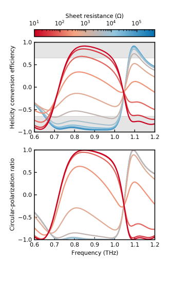
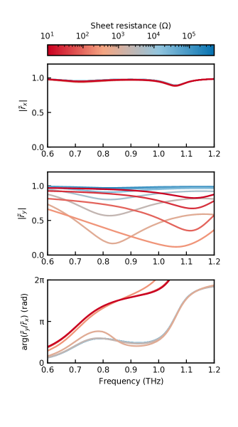
Figure S1 represents the VO2-resistance dependency of the helicity conversion efficiency and circular polarization ratio for the original design. The gradual transition between the off and on states can be observed. Figure S2 shows the corresponding reflection amplitude and phase. The reflection remains unchanged as the current barely flows in VO2. On the other hand, has dissipation in the intermediate states due to ohmic loss. The transition of the resonant frequency induces a phase jump in .
6 Stability of the fabricated device
Figures S3, S4 (used in the manuscript), and S5 show the device characteristics measured at different cycles on three different days. These data certainly confirm the reproducibility of our device. No performance degradation is observed in the cycles. Note that we did not fill the sample box with dry air for the data shown in Figure S3; thus, the data show dips of terahertz absorption by water.