An Endless Optical Phase Delay for Phase Synchronization in High-Capacity DCIs
Abstract
In this work, we propose and demonstrate a module to linearly add an arbitrary amount of continuous (reset-free) phase delay to an optical signal. The proposed endless optical phase delay (EOPD) uses an optical IQ modulator and control electronics (CE) to add the desired amount of phase delay that can continuously increase with time. In order to adjust for the bias voltages and control voltage amplitudes in the EOPD, some of which may be time varying, a multivariate gradient descent algorithm is used. The EOPD has been demonstrated experimentally, and its use in a high-capacity data center interconnect (DCI) application has been outlined in this letter. The EOPD may find its use in many other applications that require precise phase/frequency adjustments in real-time.
Index Terms:
Continuous phase modulation, coherent communication, electro-optic phase modulator, gradient descent.I Introduction
Electro-optic phase modulators (PMs) are essential components in optical communication links, optical wireless access networks, and radars and beam-forming antenna phased arrays based transceivers [1, 2, 3]. The PMs in these systems are used for (but not limited to) generating optical phase shift, phase synchronization, frequency comb generation, and frequency stabilization of lasers [4, 5, 6]. Depending on the application, PMs are evaluated based on the performance metrics that include drive voltage, half-wave voltage, electrical modulation bandwidth, optical bandwidth, dynamic range, extinction ratio (modulation depth), and linearity [7]. Various PMs with high-performance parameters such as high bandwidth, high linearity, high modulation efficiency, and low-loss have been discussed in the literature. However, the maximum amount of phase change provided by these conventional PMs is limited due to constraints on the magnitude of the electrical drive signal that can be applied and material properties of the modulator as they typically follow the relation: , wherein , , and represent the phase of the output signal, applied drive voltage, and half-wave voltage of the PM, respectively. If a tunable phase shift of upto can be provided by the PM, any phase shift can be achieved in theory. However, if the phase shift has to be changed continuously with time, these PMs cannot be used.
A few approaches have been proposed in the literature for generating an infinite amount of phase delay over the time, which is called endless (or boundless) phase delay. A demonstration shown in [8] is implemented on an integrated platform comprising multiple phase shifters and directional couplers in a cascade, which requires control signals that are difficult to synthesize for high-speed error-free phase delay generation. Another architecture, described in [9], uses a series of Mach-Zehnder interferometer (MZI) switches, comprising phase shifters and a line phase shifter along with multiple analog control signals to generate the desired phase shift. Here, the main limitation is the requirement of a large number of components and electrical signals that have to be controlled precisely. The phase delay generator demonstrated in [10], uses the principle of serrodyning with time shift and phase shift approaches. However, the system exhibits large relative phase fluctuations due to temperature variations and requires precise control of optical and electrical signals. Also, it requires switching of the optical signal, which makes it less suitable for practical applications.
In this work, we propose an optical IQ modulator based module, along with a methodology to generate control signals, to achieve an EOPD that can be used in practical applications. The proposed module overcomes most of the limitations associated with the existing endless phase delay techniques. To overcome the non-idealities of the IQ modulator, an optimization procedure has been proposed and detailed. Experimental characterization of the EOPD and its use for phase offset correction in a polarization multiplexed carrier based self-homodyne (PMC-SH) link have also been presented.
II EOPD Architecture
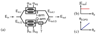
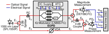
The proposed EOPD, shown in Fig. 1(a), comprises an IQ modulator, having two Mach-Zehnder modulators (MZMs) (one each in the I and the Q arms) and a PM embedded in the Q-arm, and CE. The CE generate the bias voltages (, , and ) and control signals ( and ), and actively adjust them to compensate for the dynamic variations. The EOPD optical input has magnitude and frequency , and generates output , which is the phase delayed version of the input (with a phase shift ). To achieve the desired phase shift , that has to be changed with time without any discontinuity, and are applied as continuous functions of time. For simplicity, we assume that each of the internal MZMs is biased at its null point, and the PM is biased to provide a phase shift of . With this assumption, we can write the following expression (without explicitly showing the biases , , and ):
| (1) | ||||
where is the half-wave voltage of each of the MZMs. The phase added by the EOPD, i.e. can be obtained from (1) and written as:
| (2) |
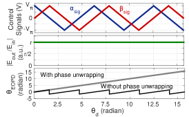
where, is the integer that unwraps the phase correctly [11]. Phase unwrapping ensures that is a continuous function of time when and are also continuous functions of time. The operating constraints for the EOPD are: (i) the magnitude constraint, i.e. the magnitude of has to be constant and (say ), irrespective of the value of , as shown in Fig. 1(b) and represented by using: (3) and (ii) the phase constraint set by (2). Considering that is ideally equal to , and using (2) and (3), we obtain and . It is important to note that multiple values of and can satisfy these constraints. However, we choose the values that keep and real, bounded, and continuous versus time, so that is also continuous with time. For , and turn out to be triangular waveforms, that have peak-to-peak amplitudes of and are delayed by one-fourth period relative to each other, as shown in simulation results (Fig. 2). The magnitude transfer function in (3) is constant (), while , monotonically increases with with phase unwrapping. An EOPD adds a phase delay to with a slope of (: frequency of control signals). Each cycle of control signals adds radians (Fig. 2) of phase shift to and with cycles, radians of phase shift can be achieved for any real value of . In order to validate the magnitude constraint, signal is given to a photodetector (PD) resulting in photocurrent proportional to (represented by ), which is required to be constant with varying . For validating the phase condition, interferometer structure comprising a coupler and a PD that acts as a photo-mixer is used. The output of the coupler is and the corresponding photocurrent, is required to be proportional to (denoted by ) and has negligible distortion.
III EOPD: Optimization and characterization
In order to bias the two MZMs of the IQ modulator at their null points, suitable biases and have to be added to and , respectively. Also, to provide a phase shift between optical signals in I and Q arms, a suitable bias has to be provided (as shown in Fig. 1(a)). To correct dynamic variations in the properties of the IQ modulator (that cause drift in , and ), the use of a multivariate iterative gradient descent algorithm has been proposed and demonstrated. We use the normalized magnitude condition as the input, with and as the actual and predicted magnitudes, respectively. The risk function J, which is the mean square difference between and is minimized by optimizing the EOPD parameters (bias voltages: , , and ; and control voltage amplitudes: and ). The procedure used for correcting is summarized in Algorithm 1. This algorithm also monitors the normalized phase condition, .
 |
|
 |
|
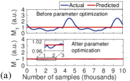
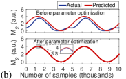
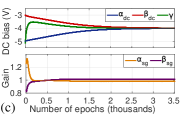
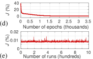
Figure 3 presents the results obtained by optimizing the EOPD parameters. Due to fluctuations in the EOPD parameters, shows huge variations, deviating from . After optimizing the parameters, approaches as shown in Fig. 3(a). Similar behavior for is observed in Fig. 3(b), showing proximate predicted and actual values. The zoomed version also emphasizes the deviation of actual value by 1% from the predicted value. With the proposed architecture and algorithm, if the EOPD parameters are optimized, both and can be corrected, simulatanously. Corresponding settling of EOPD parameters is observed in Fig. 3(c). Convergence of J shown in Fig. 3(d) signifies its minimization from 40% to 0.1%. The simulation is run for one thousand different cases of variations of , and the minimization of J is plotted in Fig. 3(e), which validates this technique’s feasibility for correcting , in the presence of deviation of EOPD parameters within a range of 30% from their nominal values. In certain cases, the risk function shows a higher order of magnitude, which is due to these parameters showing variations greater than 30% from their nominal values. Such aberration is associated with J as it is not strictly convex (verified using Hessian matrix, which was not positive definite). To resolve this issue, when J crosses a certain threshold, the EOPD parameters are reset.
Experimental setup to validate the EOPD operation is shown in Fig. 4. A laser output is split to generate and . is given to the IQ modulator, which receives biases and control signals from DC supply and arbitrary function generator (AFG), respectively. The , , and are set to , , and , respectively with and having peak to peak swing of and a frequency of 1 MHz. In this configuration, the combination of IQ modulator and CE acts as EOPD generating . is equally split separately for validating the magnitude and the phase conditions to give out and . fed to PD1 generates photocurrent and is converted into . is combined with and then given to PD2 forming an interferometer. The interferometer output is converted into voltage using 50 load. These waveforms are observed on an oscilloscope.
 |
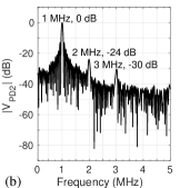 |
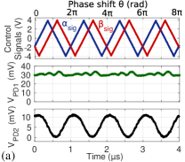
Experimental results of EOPD are shown in Fig. 5. Control signals of 1 MHz introduce a phase delay to the input signal at a rate of rads. The waveform, signifying the behavior of magnitude condition, is approximately constant. The interferometer output is a 1 MHz sinusoidal signal signifying the addition of a phase delay at a rate of rad/s over time. This behavior is similar to phase accumulation at a rate of per cycle as observed in Fig. 2. The frequency spectrum of depicted in Fig. 5(b), which shows that the fundamental frequency is at least 20 dB above its harmonics validating phase condition. The EOPD’s operation conditions can be improved further by incorporating a lookup table in the algorithm to take care of second order effects in the modulator.
IV EOPD for Phase Synchronization in a DCI
The EOPD can be used for many applications, such as optical frequency shifting [12], MIMO demultiplexing [9], multi-carrier generation [13], RF sinusoidal signal generation using optical phase locked loops [14], and carrier phase synchronization in coherent homodyne and self-homodyne links [15].
EOPD aided phase synchronization
In PMC-SH links, the modulated signal () and the unmodulated carrier () co-propagate along the same channel in two orthogonal polarizations and are separated at the receiver for demodulation [16]. Due to the path length difference, laser linewidth, and polarization mode dispersion, time varying phase offset is introduced between and , which has to be removed using phase synchronization. Analog signal processing based phase synchronization technique with the aid of conventional PM is demonstrated in [6]. However, due to the bounded phase delay provided by conventional PM, the loop fails to track the phase offset when it exceeds a few radians. Under such conditions, EOPD is a solution to synchronize the phases of and .
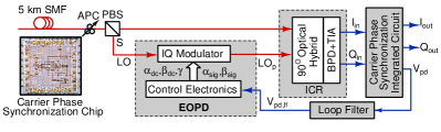
An experimental setup of the PMC-SH system with EOPD based phase synchronization is shown in Fig. 6. At the receiver side of the PMC-SH link, and are obtained after adaptive polarization control (APC). The EOPD takes and gives out a phase delayed version . The and are mixed and down-converted to baseband in-phase and quadrature-phase electrical signals and , where and denote message phase and time varying phase offset, respectively. These signals are given to analog domain proof-of-concept phase synchronization chip that generates phase detector output , which is proportional to . The is given to the EOPD through loop filter. The CE generates bias voltages and control signals corresponding to the . EOPD adds phase delay to to generate based on the control signals’ phase/frequency. At steady state, in closed loop condition, the phases of control signals are such that the phase delay added to is equal and opposite to resulting in phase alignment of and and hence obtaining and , which are phase offset corrected signals obtained at the output of the phase synchronization chip.
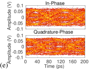
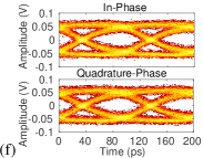
Experimental results obtained with 20 Gbps PMC-SH QPSK system are presented in Fig. 7. In open loop condition, shows a swing of 400 mV (shown in Fig. 7(a)) and corresponding EOPD control signals are triangular, as shown in Fig. 7(c). As a result, the in-phase and quadrature-phase signals show closed eye-diagrams, as shown in Fig. 7(e). In closed loop condition, the signal shows lower amplitude (shown in Fig. 7(b)) resulting in continuously time varying control signals (shown in Fig. 7(d)). Such behavior of , , and signify continuous tracking of phase offset by the loop. Closing the loop results in opening of the eye, as shown in Fig. 7(f) due to phase offset correction. The proposed EOPD aided carrier phase synchronization is independent of data rate as EOPD aims at correcting . This proof-of-concept demonstration is done at 20 Gbps due to frequency limitations posed by the analog domain carrier phase synchronization chip and the PCB assembly. The power dissipation of the proposed EOPD can range from less than a milliwatt to a few tens of milliwatts depending on the speed of phase shift that has to be changed, the type of phase shifters, and electronics used.
 |
 |
V Conclusion
We presented an EOPD that can add an arbitrary amount of phase delay to an optical signal. The EOPD can be tuned seamlessly and achieve an infinite delay range. The EOPD can be used in many practical applications, including phase/frequency shifting in coherent links and DCIs (one such application was presented). The EOPD can also be employed in LiDAR and multiple phased antenna array receiver applications.
References
- [1] K.-P. Ho, Phase-modulated optical communication systems. Springer Science & Business Media, 2005.
- [2] J. Yu, G. K. Chang, Z. Jia, L. Yi, Y. Su, and T. Wang, “A ROF downstream link with optical mm-wave generation using optical phase modulator for providing broadband optical-wireless access service,” in Proc. OFC., 2006, p. OFM3.
- [3] V. M. Hietala, G. A. Vawter, W. J. Meyer, and S. H. Kravitz, “Phased-array antenna control by a monolithic photonic integrated circuit,” in Proc. SPIE, vol. 1476, 1991, pp. 170 – 175.
- [4] R. Wu, V. R. Supradeepa, C. M. Long, D. E. Leaird, and A. M. Weiner, “Generation of very flat optical frequency combs from continuous-wave lasers using cascaded intensity and phase modulators driven by tailored radio frequency waveforms,” Opt. Lett., vol. 35, no. 19, pp. 3234–3236, Oct 2010.
- [5] Y. Ji et al., “A Phase Stable Short Pulses Generator Using an EAM and Phase Modulators for Application in 160-GBaud DQPSK Systems,” IEEE Photon. Technol. Lett., vol. 24, no. 1, pp. 64–66, 2012.
- [6] R. Ashok, S. Manikandan, S. Chugh, S. Goyal, R. Kamran, and S. Gupta, “Demonstration of an Analogue Domain Processing IC for Carrier Phase Recovery and Compensation in Coherent Links,” in Proc. OFC., 2019, pp. 1–3.
- [7] R. G. Hunsperger, Integrated Optics: Theory and Technology, 6th ed. Springer Publishing Company, Incorporated, 2009.
- [8] C. K. Madsen, “Boundless-Range Optical Phase Modulator for High-Speed Frequency-Shift and Heterodyne Applications,” J. Lightw. Technol., vol. 24, no. 7, p. 2760, Jul 2006.
- [9] C. Doerr, “Endless phase shifting,” Jul. 22 2014, US Patent 8,787,708.
- [10] S. Ozharar, F. Quinlan, S. Gee, and P. J. Delfyett, “Demonstration of endless phase modulation for arbitrary waveform generation,” IEEE Photon. Technol. Lett., vol. 17, no. 12, pp. 2739–2741, 2005.
- [11] A. Oppenheim and G. Verghese, Signals, Systems and Inference, Global Edition. Pearson Education Limited, 2016.
- [12] M. Izutsu, S. Shikama, and T. Sueta, “Integrated optical SSB modulator/frequency shifter,” IEEE J. Quantum Electron., vol. 17, no. 11, pp. 2225–2227, 1981.
- [13] H. Yamazaki et al., “Dual-Carrier Dual-Polarization IQ Modulator Using a Complementary Frequency Shifter,” IEEE J. Quantum Electron., vol. 19, no. 6, pp. 175–182, 2013.
- [14] K. Balakier, L. Ponnampalam, M. J. Fice, C. C. Renaud, and A. J. Seeds, “Integrated Semiconductor Laser Optical Phase Lock Loops,” IEEE J. Sel. Topics Quantum Electron., vol. 24, no. 1, pp. 1–12, 2018.
- [15] R. Ashok, R. Kamran, S. Naaz, and S. Gupta, “Demonstration of a PMC-SH link using a phase recovery IC for low-power high-capacity DCIs,” in Proc. CLEO., 2020, p. SF3L.3.
- [16] R. Kamran, S. Naaz, S. Goyal, and S. Gupta, “High-Capacity Coherent DCIs Using Pol-Muxed Carrier and LO-Less Receiver,” J. Lightw. Technol., vol. 38, no. 13, pp. 3461–3468, 2020.