Enhanced electron-phonon coupling in doubly aligned hexagonal boron nitride bilayer graphene heterostructure
Abstract
The relative twist angle in heterostructures of two-dimensional (2D) materials with similar lattice constants result in a dramatic alteration of the electronic properties. Here, we investigate the electrical and magnetotransport properties in bilayer graphene (BLG) encapsulated between two hexagonal boron nitride (hBN) crystals, where the top and bottom hBN are rotationally aligned with bilayer graphene with a twist angle , respectively. This results in the formation of two moiré superlattices, with the appearance of satellite resistivity peaks at carrier densities and , in both hole and electron doped regions, together with the resistivity peak at zero carrier density. Furthermore, we measure the temperature(T) dependence of the resistivity (). The resistivity shows a linear increment with temperature within the range 10K to 50K for the density regime with a large slope d/dT 8.5 /K. The large slope of d/dT is attributed to the enhanced electron-phonon coupling arising due to the suppression of Fermi velocity in the reconstructed minibands, which was theoretically predicted, recently in doubly aligned graphene with top and bottom hBN. Our result establishes the uniqueness of doubly aligned moire system to tune the strength of electron-phonon coupling and to modify the electronic properties of multilayered heterostructures.
I Introduction
Rotational alignment between atomically thin two-dimensional (2D) crystals leads to artificial superlattice potential forming moiré patternsNovoselov et al. (2016). One well established example is graphene on hexagonal boron nitride (hBN).
The weak periodic potential due to underlying hBN gives rise to modulation of graphene electronic band structure Yankowitz et al. (2012, 2019); Kumar et al. (2018), with the emergence of clone Dirac conesHunt et al. (2013), wherein, the Fermi velocity could be controlled by the relative twist angle between graphene and hBN, showing interesting physics like the Hofstader butterfly (Dean et al., 2013), resonant tunnelingMishchenko et al. (2014), change of topological winding numberWang et al. (2015), topological valley currentEndo et al. (2019), Brown-Zak oscillationsPonomarenko et al. (2013)etc. Moreover, twisting individual layers leads to flat bands Bistritzer and MacDonald (2011), where emergent phenomenon like correlated insulating stateCao et al. (2018a), superconductivityCao et al. (2018b), quantum anomalous Hall effectSerlin et al. (2020), fractional Chern insulating statesChen et al. (2020); Repellin and Senthil (2019), moiré excitonsTran et al. (2019), and ferromagnetismSerlin et al. (2020) has been observed. Furthermore, in multilayered heterostructures, competing moiré superlattice could be present, due to the lattice mismatch between individual layers which can lead to further dramatic change in the electronic propertiesWang et al. (2019a, b).
Alternatively, another concomitant way to engineer moiré superlattice is to exploit the rotational alignment of graphene with both top and bottom hBN. This could result in two moiré superlattice structures of wavelength and , respectively. The interference of these two moiré superlattices could result in a supermoiré structure of wavelength . The supermoiré wavelength can vary from 1 nm to infinity, depending on the rotational alignment of graphene with top (bottom) hBNWang et al. (2019a). Recently, the transport measurements have been carried out for hBN/graphene/hBN doubly aligned heterostructures and the signature of supermoiré patterns have been observedWang et al. (2019b). Furthermore, in refAnđelkovic et al. (2020) it has been theoretically predicted the band is less dispersive with reduced Fermi velocity for the minibands in doubly aligned hBN/graphene/hBN heterostructures. Since the BLG has a parabolic dispersion, it is expected to exhibit a further reduction in Fermi velocity in doubly aligned hBN/BLG/hBN heterostructures as compared to the monolayer counterpart. However, there are no experimental studies on this kind of structures.
Here, we study the low temperature electrical transport in a hBN/BLG/hBN heterostructure, where the top and bottom hBN are rotationally aligned with BLG with a twist angle , respectively. The low-temperature transport shows the emergence of additional satellite resistivity peaks at carrier densities () in hole as well as electron doped regions, together with the intrinsic resistivity peak at zero carrier density. The Hall resistance at low magnetic field shows expected sign change at these peak positions. Furthermore, we study the temperature dependence of resistivity as a function of carrier density. We find that resistivity () varies with temperature as for different carrier densities. Interestingly, we find that, in the density regime between , the measured resistivity varies linearly () with temperature within the range 10K to 50K. The slope of resistivity (d/dT) in this linear regime was found to be maximum of K. This value is approximately two orders of magnitude higher than pristine graphene with d/dTKChen et al. (2008); Efetov and Kim (2010); Hwang and Das Sarma (2008). The linear dependence of resistivity with temperature arises due to the electron-acoustic phonon scatteringHwang and Das Sarma (2008); Wu et al. (2019). It was recently shown theoretically in refAnđelkovic et al. (2020), that in doubly aligned hBN/graphene/hBN heterostructures, the minibands are less dispersive with reduced Fermi velocity in the density regime . In our device, we attribute the higher value of d/dT to the enhanced electron-phonon coupling resulting from the suppression of Fermi velocity in these minibands.
II Results and Discussion
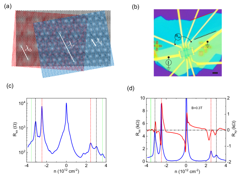
We fabricated bilayer graphene (BLG) devices encapsulated between two hexagonal boron nitride crystals using the dry transfer techniqueWang et al. (2013); Kuiri et al. (2018); Kuiri and Das (2019). The fabrication technique is similar to our earlier workKumar et al. (2016, 2018); Kuiri and Das (2019). In addition, the BLG edge was carefully aligned with the
crystallographic axes of both top (bottom) hBN. The natural rectangular shape of bilayer graphene allowed us to pattern the device into a Hall bar geometry. Edge contacts were established by standard electron beam lithography followed by thermal deposition of Cr/Pd/Au (2/10/70)nm. The optical image of the device is shown in Fig.1(b). The measurements were carried out in 3He cryostat using standard lock-in technique, in a four-terminal configuration as schematically shown in Fig. 1(b).
Figure 1(a) shows the illustration of the appearance of moiré pattern, where the two crystals, BLG and hBN are aligned relative to one another (, with top hBN) and (, with bottom hBN). The relative rotation between the two crystals defines the moiré wavelength . The appearance of supermoiré structure has been illustrated in Fig. 1(a). In our device the top hBN is nearly perfectly aligned with bilayer graphene (), whereas the bottom hBN has slightly different twist angle (). Fig. 1(c) shows the four terminal longitudinal resistance as a function of carrier density () at T 250mK. The estimated mobility of our device was found to be /Vs(Supplemental Materialsup ). In addition to the resistance peak at primary Dirac point (PDP), we also observe two strong resistance peak at and , highlighted by red and black dashed vertical line in Fig. 1(c), respectively. The resistance peaks corresponding to densities and originate due to the two different moiré superlattice potentials arising from the rotational alignment of top and bottom hBN with BLG. We attribute the satellite resistance peaks corresponding to densities , as secondary Dirac point 1 (SDP1) and secondary Dirac point 2 (SDP2), respectively. It was reported that the second satellite peak (SDP2) may appear even in single aligned graphene/hBN heterostructure due to formation of Kekule superstructure with . However, for our device . Thus, we rule out the origin of SDP2 due to the formation of Kekule superstructure. It is worth to mention here that the spatial distribution of the twist angles over the sample should be uniform to observe the strong side resistivity peaks.
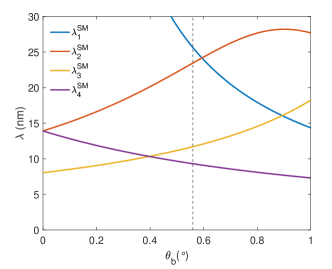
In contrast to the strong resistance peak in the hole doped regime, weak resistance peaks are observed in the electron doped regime, at similar densities. This asymmetry in electron-hole transport in BLG/hBN moiré devices arises because the hBN induces different onsite energies, which is stronger for hole band as compared to the electron bandYankowitz et al. (2012); DaSilva et al. (2015); Anđelkovic et al. (2020). The electron-hole asymmetry has also been observed experimentallyYankowitz et al. (2012); Wang et al. (2019b) and calculated theoreticallyAnđelkovic et al. (2020) for monolayer graphene aligned with two hBN, citing a similar origin. Now, from the carrier density of the satellite peak, we can estimate moiré wavelength () given by . The resistance peak corresponding to carrier density shows a perfect alignment of BLG with top hBN () with a moiré wavelength of nm. Similarly, the resistance peak at corresponds to a moiré wavelength of nm (). The interference of these two moiré superlattices could result in the formation of supermoiré structure. In refAnđelkovic et al. (2020), the supermoiré wavelengths have been theoretically calculated based on four possible reciprocal lattice vectors configurations. For our device and , the possible supermoiré wavelengths are 25.6, 23.4, 11.7 and 9.3nm(Supplemental Materialsup ). The resistance peaks observed in our experiment at (marked as green dotted line in Fig.1c) corresponds to moiré wavelength of 11.5nm, which matches closely with one of the supermoiré wavelength (11.7nm). However, weak shoulder at does not match with any supermoiré wavelength. In refWang et al. (2019b), it was proposed that these peaks could be due to more exotic superlattice phenomena or higher order moiré periodicities. Fig. 1(d) shows the Hall resistance as a function of carrier density for a perpendicular magnetic field of B=0.3T. As one would expect the charge carriers change from hole-like to electron like when crossing both the charge neutrality , and at superlattice gaps for , and . We would also like to note that, the Hall resistance changes sign at , which corresponds to the supermoiré wavelength of 11.7nm, highlighted by green dotted vertical line in Fig. 1(d).
III Magnetic field data
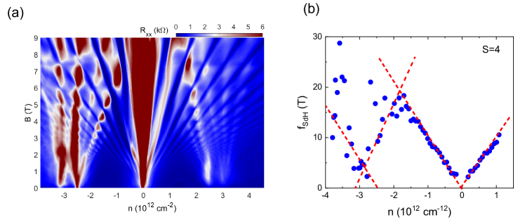
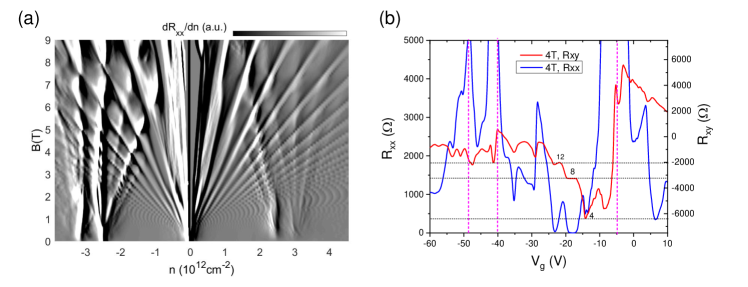
We measure the Hall resistance, and the longitudinal resistance, as a function of a perpendicular magnetic field (B) and carrier density (). We observe quantum oscillations evolving from PDP, SDP1, and SDP2 for both electron and hole side. Fig. 2(a) shows the measured as a function of carrier density and magnetic field for both electron and hole-doped regions. The sequence of verifies that indeed our flake is bilayer graphene (Supplemental Materialsup ). Alternatively, we extract the Shubnikov de Haas (SdH) oscillation frequency (), from which we can calculate the Landau level(LL) degeneracy for and for Cao et al. (2018a). The SdH oscillation frequency is given by , where, S represents the degeneracy of the Landau levels. In BLG, due to the spin and valley degeneracy S=4. Fig. 2(b) shows the measured oscillation frequency as a function of carrier density. Near PDP, we obtain , revealing the observed fillings at , consistent with the LL spectrum of intrinsic bilayer graphene. Similarly, the LL fan for and also has a degeneracy of S=4.
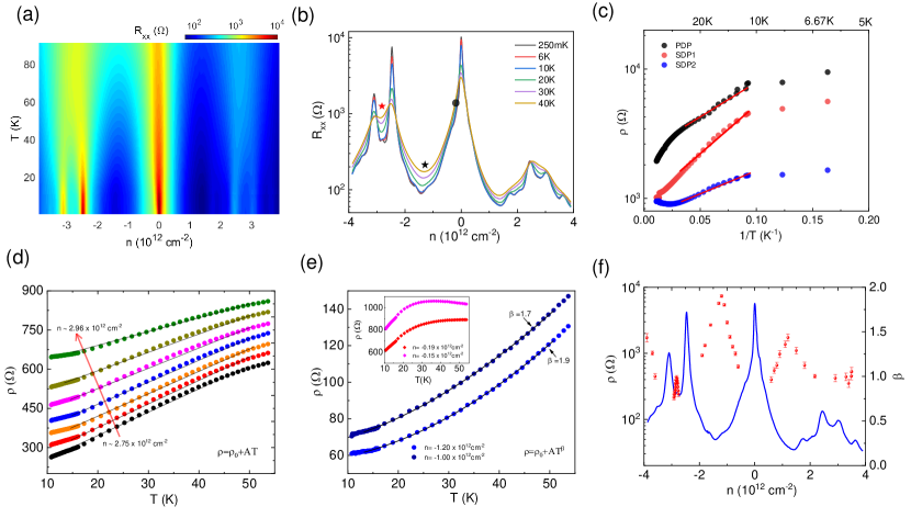
IV Temperature Dependence
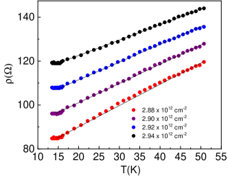
The dependence of material’s resistivity with temperature reveals important physics related to carrier scattering, electron-phonon coupling, and electron-electron interactions in the systemHartnoll (2015). Fig. 3(a) shows the 2D colorplot of , as a function of carrier density (). Insulating behavior was observed at PDP, SDP1, and SDP2. Fig. 3(b) shows the line cut of Fig. 3(a) at several temperatures. It can be seen that the resistivity increases with the increase in temperature close to in between SDP1, and SDP2 signifying metallic transport. Fig. 3(c) shows the Arrhenius plot vs 1/T at PDP, SDP1, and SDP2. Activated transport is observed for PDP and SDP1. However, although the SDP2 shows activated behavior at low temperature, the resistivity increases at high temperatures. The linear fit with the Arrhenius equation gives a gap of meV and meV for SDP1, and SDP2, respectively. In Fig. 3(d), we show with T, for several values of between and . We see that evolves linearly with T up to T 50K. We fit our temperature dependence data in the range of 10K to 50K with . We find that in the region between , with , and a maximum value of (A) is found to be A=d/dTK. In Fig. 3(e) we show the -T for few other densities. It can be seen in Fig. 3(e), that in the region between PDP and SDP1, reaches upto 1.9. Close to PDP, resistivity increases non monotonically with temperature, as can be seen in the inset of Fig. 3e.
The value of d/dT in the regime is nearly two orders of magnitude larger as compared to intrinsic monolayer graphene with d/dTKChen et al. (2008); Efetov and Kim (2010); Hwang and Das Sarma (2008). It is worth to mention here that the resistivity of intrinsic bilayer graphene shows a very weak dependence on temperatureDean et al. (2010); Hwang and Das Sarma (2010).In Fig. 3(f), we plot as a function of carrier density. It can be seen that , in the region between in the hole doped region. Qualitatively, similar behavior was observed in electron doped regime with a smaller value of d/dTK (Supplemental materialsup ). However, at all other densities , changes significantly with the change in carrier densities as can be seen in Fig. 3(f). Recently, it has been shown theoreticallyAnđelkovic et al. (2020), that in the doubly aligned hBN/graphene/hBN heterostructures, reconstruction of band structures gives rise to the formation of less dispersive minibands with reduced Fermi velocity. Now having BLG in our device over mono layer, could imply further reduction in Fermi velocity since the low energy dispersion is parabolic in BLG. Thus one expects further reduction in Fermi velocity for hBN/BLG/hBN heterostructures. This could give rise to large electron-phonon coupling similar to what has been observed in twisted bilayer graphene devicesPolshyn et al. (2019). Due to this enhanced electron-phonon coupling, we observe the large d/dT of K in the density regime . To compare our results with mono layer graphene, we follow the similar approach, which was used for monolayer graphene and twisted bilayer graphene. Theoretically, the resistivity at high T, due to acoustic phonon induced scattering is given byHwang and Das Sarma (2008); Wu et al. (2019)
| (1) |
Where D, , , and are the deformation potential, phonon velocity, Fermi velocity of graphene, and atomic mass density, respectively. are the spin(valley) degeneracy. For pristine graphene , , , and eV yields d/dTKChen et al. (2008); Efetov and Kim (2010); Hwang and Das Sarma (2008). Since the phonon spectrum remains relatively invariant in moiré systemChoi and Choi (2018); Wu et al. (2019), is assumed to be constant. Therefore, using the above values for , , and the experimentally measured value of d/dTK, we estimate the renormalized Fermi velocity m/s. Please note that, different values of eV are quoted in theoryHwang and Das Sarma (2008) and even this uncertainty in can not explain the nearly two order of magnitude enhancement in d/dT. We would also like to mention that temperature broadening and the excitation of carriers across the minigaps could affect the temperature dependence of resistivity. However, in our device, we believe that this would not affect significantly due to following reason. The SDP1 and SDP2 peaks are separated by an energy interval of 25 meV(Supplemental Materialsup ). Since, we have performed our analysis near the middle of the two secondary peaks, which is 12 meV away from SDP1 and SDP2. The estimated width of the SDP1 and SDP2 was found to be 1meV and 1.5meV, respectively (Supplemental Materialsup ), which is less compared to the temperature broadening of 4.3 meV at 50K. This suggests that the temperature broadening effect will be dominant only near the SDP1 and SDP2 in energy window of 4meV, and it will not affect significantly near the density regime, where we have performed our analysis. Therefore, we attribute the large d/dT to the suppression of in the reconstructed bands, as a plausible expansion. This reduced Fermi velocity, in our device, is not surprising. As discussed earlier it could be due to the formation of narrow bands which has been theoretically predicted in doubly aligned graphene devices with hBN. Our result, therefore, hints on a perspective of creating an alternative framework for narrow bands using doubly aligned graphene on hBN devices. Further experimental and theoretical work is desirable to explore the band structure of doubly aligned bilayer graphene devices, and to explore the possibility of obtaining flat dispersion, which could be an interesting platform to study strong interaction physics or superconductivity as observed in twisted bilayer grapheneCao et al. (2018b).
V Conclusion
In summary, we have presented the electrical and magneto-transport properties of doubly aligned hBN/BLG/hBN moiré heterostructure. We observe the appearance of strong resistivity peaks due to the presence of two moiré wavelengths. We show that the temperature dependence of resistivity scales linearly with T in the region , with slope of nearly two orders of magnitude larger than pristine graphene.
VI Acknowledgement
The authors would like to acknowledge the Center for Nanoscience and Engineering (CENSE), IISc for fabrication facilities. S.K.S. acknowledges PMRF, MHRD for financial support. A.D. thanks the Department of Science and Technology (DST), India for financial support (DSTO-2051) and acknowledges the Swarnajayanti Fellowship of the DST/SJF/PSA-03/2018-19. A.D. also acknowledges supports from the MHRD, Govt. of India under STARS research funding (STARS/APR2019/PS/156/FS).
References
- Novoselov et al. (2016) K. Novoselov, A. Mishchenko, A. Carvalho, and A. C. Neto, 2d materials and van der waals heterostructures, Science 353 (2016).
- Yankowitz et al. (2012) M. Yankowitz, J. Xue, D. Cormode, J. D. Sanchez-Yamagishi, K. Watanabe, T. Taniguchi, P. Jarillo-Herrero, P. Jacquod, and B. J. LeRoy, Emergence of superlattice dirac points in graphene on hexagonal boron nitride, Nature Physics 8, 382 (2012).
- Yankowitz et al. (2019) M. Yankowitz, Q. Ma, P. Jarillo-Herrero, and B. J. LeRoy, van der waals heterostructures combining graphene and hexagonal boron nitride, Nature Reviews Physics 1, 112 (2019).
- Kumar et al. (2018) C. Kumar, S. K. Srivastav, P. Adhikary, S. Banerjee, T. Das, and A. Das, Localization physics in graphene moiré superlattices, Phys. Rev. B 98, 155408 (2018).
- Hunt et al. (2013) B. Hunt, J. Sanchez-Yamagishi, A. Young, M. Yankowitz, B. J. LeRoy, K. Watanabe, T. Taniguchi, P. Moon, M. Koshino, P. Jarillo-Herrero, et al., Massive dirac fermions and hofstadter butterfly in a van der waals heterostructure, Science 340, 1427 (2013).
- Dean et al. (2013) C. R. Dean, L. Wang, P. Maher, C. Forsythe, F. Ghahari, Y. Gao, J. Katoch, M. Ishigami, P. Moon, M. Koshino, et al., Hofstadter’s butterfly and the fractal quantum hall effect in moire superlattices, Nature 497, 598 (2013).
- Mishchenko et al. (2014) A. Mishchenko, J. Tu, Y. Cao, R. Gorbachev, J. Wallbank, M. Greenaway, V. Morozov, S. Morozov, M. Zhu, S. Wong, et al., Twist-controlled resonant tunnelling in graphene/boron nitride/graphene heterostructures, Nature Nanotechnology 9, 808 (2014).
- Wang et al. (2015) P. Wang, B. Cheng, O. Martynov, T. Miao, L. Jing, T. Taniguchi, K. Watanabe, V. Aji, C. N. Lau, and M. Bockrath, Topological winding number change and broken inversion symmetry in a hofstadter’s butterfly, Nano Lett. 15, 6395 (2015).
- Endo et al. (2019) K. Endo, K. Komatsu, T. Iwasaki, E. Watanabe, D. Tsuya, K. Watanabe, T. Taniguchi, Y. Noguchi, Y. Wakayama, Y. Morita, et al., Topological valley currents in bilayer graphene/hexagonal boron nitride superlattices, Appl. Phys. Lett. 114, 243105 (2019).
- Ponomarenko et al. (2013) L. Ponomarenko, R. Gorbachev, G. Yu, D. Elias, R. Jalil, A. Patel, A. Mishchenko, A. Mayorov, C. Woods, J. Wallbank, et al., Cloning of dirac fermions in graphene superlattices, Nature 497, 594 (2013).
- Bistritzer and MacDonald (2011) R. Bistritzer and A. H. MacDonald, Moiré bands in twisted double-layer graphene, PNAS 108, 12233 (2011).
- Cao et al. (2018a) Y. Cao, V. Fatemi, A. Demir, S. Fang, S. L. Tomarken, J. Y. Luo, J. D. Sanchez-Yamagishi, K. Watanabe, T. Taniguchi, E. Kaxiras, et al., Correlated insulator behaviour at half-filling in magic-angle graphene superlattices, Nature 556, 80 (2018a).
- Cao et al. (2018b) Y. Cao, V. Fatemi, S. Fang, K. Watanabe, T. Taniguchi, E. Kaxiras, and P. Jarillo-Herrero, Unconventional superconductivity in magic-angle graphene superlattices, Nature 556, 43 (2018b).
- Serlin et al. (2020) M. Serlin, C. Tschirhart, H. Polshyn, Y. Zhang, J. Zhu, K. Watanabe, T. Taniguchi, L. Balents, and A. Young, Intrinsic quantized anomalous hall effect in a moiré heterostructure, Science 367, 900 (2020).
- Chen et al. (2020) G. Chen, A. L. Sharpe, E. J. Fox, Y.-H. Zhang, S. Wang, L. Jiang, B. Lyu, H. Li, K. Watanabe, T. Taniguchi, et al., Tunable correlated chern insulator and ferromagnetism in a moiré superlattice, Nature 579, 56 (2020).
- Repellin and Senthil (2019) C. Repellin and T. Senthil, Chern bands of twisted bilayer graphene: fractional chern insulators and spin phase transition, arXiv preprint arXiv:1912.11469 (2019).
- Tran et al. (2019) K. Tran, G. Moody, F. Wu, X. Lu, J. Choi, K. Kim, A. Rai, D. A. Sanchez, J. Quan, A. Singh, et al., Evidence for moiré excitons in van der waals heterostructures, Nature 567, 71 (2019).
- Wang et al. (2019a) L. Wang, S. Zihlmann, M.-H. Liu, P. Makk, K. Watanabe, T. Taniguchi, A. Baumgartner, and C. Schoenenberger, New generation of moire superlattices in doubly aligned hbn/graphene/hbn heterostructures, Nano Lett. 19, 2371 (2019a).
- Wang et al. (2019b) Z. Wang, Y. B. Wang, J. Yin, E. Tovari, Y. Yang, L. Lin, M. Holwill, J. Birkbeck, D. Perello, S. Xu, et al., Composite super-moiré lattices in double-aligned graphene heterostructures, Science advances 5, eaay8897 (2019b).
- Anđelkovic et al. (2020) M. Anđelkovic, S. P. Milovanovicc, L. Covaci, and F. M. Peeters, Double moiré with a twist: Supermoiré in encapsulated graphene, Nano Letters 20, 979 (2020).
- Chen et al. (2008) J.-H. Chen, C. Jang, S. Xiao, M. Ishigami, and M. S. Fuhrer, Intrinsic and extrinsic performance limits of graphene devices on sio2, Nature Nanotechnology 3, 206 (2008).
- Efetov and Kim (2010) D. K. Efetov and P. Kim, Controlling electron-phonon interactions in graphene at ultrahigh carrier densities, Phys. Rev. Lett. 105, 256805 (2010).
- Hwang and Das Sarma (2008) E. H. Hwang and S. Das Sarma, Acoustic phonon scattering limited carrier mobility in two-dimensional extrinsic graphene, Phys. Rev. B 77, 115449 (2008).
- Wu et al. (2019) F. Wu, E. Hwang, and S. Das Sarma, Phonon-induced giant linear-in- resistivity in magic angle twisted bilayer graphene: Ordinary strangeness and exotic superconductivity, Phys. Rev. B 99, 165112 (2019).
- Wang et al. (2013) L. Wang, I. Meric, P. Huang, Q. Gao, Y. Gao, H. Tran, T. Taniguchi, K. Watanabe, L. Campos, D. Muller, et al., One-dimensional electrical contact to a two-dimensional material, Science 342, 614 (2013).
- Kuiri et al. (2018) M. Kuiri, G. K. Gupta, Y. Ronen, T. Das, and A. Das, Large landau-level splitting in a tunable one-dimensional graphene superlattice probed by magnetocapacitance measurements, Phys. Rev. B 98, 035418 (2018).
- Kuiri and Das (2019) M. Kuiri and A. Das, Energetics of the complex phase diagram of a tunable bilayer graphene probed by quantum capacitance, Phys. Rev. B 99, 125411 (2019).
- Kumar et al. (2016) C. Kumar, M. Kuiri, J. Jung, T. Das, and A. Das, Tunability of 1/f noise at multiple dirac cones in hbn encapsulated graphene devices, Nano Lett. 16, 1042 (2016).
- (29) Supplemental material. The Supplemental Material contains Refs. Hwang and Das Sarma (2010); Anđelkovic et al. (2020) .
- Chen et al. (2017) G. Chen, M. Sui, D. Wang, S. Wang, J. Jung, P. Moon, S. Adam, K. Watanabe, T. Taniguchi, S. Zhou, et al., Emergence of tertiary dirac points in graphene moiré superlattices, Nano Lett. 17, 3576 (2017).
- DaSilva et al. (2015) A. M. DaSilva, J. Jung, S. Adam, and A. H. MacDonald, Transport and particle-hole asymmetry in graphene on boron nitride, Phys. Rev. B 91, 245422 (2015).
- Hartnoll (2015) S. A. Hartnoll, Theory of universal incoherent metallic transport, Nature Physics 11, 54 (2015).
- Dean et al. (2010) C. R. Dean, A. F. Young, I. Meric, C. Lee, L. Wang, S. Sorgenfrei, K. Watanabe, T. Taniguchi, P. Kim, K. L. Shepard, et al., Boron nitride substrates for high-quality graphene electronics, Nature Nanotechnology 5, 722 (2010).
- Hwang and Das Sarma (2010) E. H. Hwang and S. Das Sarma, Insulating behavior in metallic bilayer graphene: Interplay between density inhomogeneity and temperature, Phys. Rev. B 82, 081409 (2010).
- Polshyn et al. (2019) H. Polshyn, M. Yankowitz, S. Chen, Y. Zhang, K. Watanabe, T. Taniguchi, C. R. Dean, and A. F. Young, Large linear-in-temperature resistivity in twisted bilayer graphene, Nature Physics 15, 1011 (2019).
- Choi and Choi (2018) Y. W. Choi and H. J. Choi, Strong electron-phonon coupling, electron-hole asymmetry, and nonadiabaticity in magic-angle twisted bilayer graphene, Phys. Rev. B 98, 241412 (2018).
Supplemental Material for Enhanced electron-phonon coupling in doubly aligned hexagonal boron nitride bilayer graphene heterostructure
Manabendra Kuiri1, Saurabh Kumar Srivastav1, Sujay Ray1, Kenji Watanabe2, Takashi Taniguchi2, Tanmoy Das1, and Anindya Das1
1Department of Physics, Indian Institute of Science, Bangalore 560012, India
2National Institute of Material Science, 1-1 Namiki, Tsukuba 305-0044, Japan
VII Device characterization
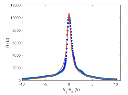
The measured four-terminal resistance () vs backgate voltage () was fitted with the equation
| (S1) |
where, , , , , and are the contact resistance, device length, device width, electronic charge and mobility, respectively. corresponds to the charge inhomogeneity. The carrier density () is given by , where , are the capacitance per unit area of the bottom gate and gate voltage at the charge neutrality point, respectively. Fig. S1 shows the fitting with Eq.(S1) near the primary Dirac point.
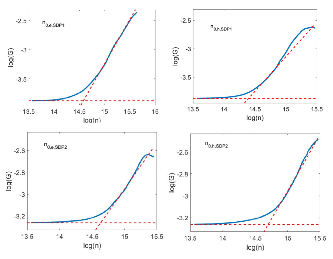
In Fig. S2, we estimate the charge inhomogeneity at SDP1 and SDP2 for the electron and the hole side. This was done by taking the log-log plot of conductance as a function of carrier density and extapolating the linear conductance on the axis. This gives carrier in-homogeneity at SDP1, and for SDP2, respectively. From this value of charge inhomogeneity, we estimate the Fermi energy broadening at SDP1 and SDP2 to be 1 meV, and 1.5 meV, respectively. We used the relation , where Hwang and Das Sarma (2010), being the electronic charge, and . The distance between the center of two peaks SDP1 and SDP2 in density axis is , which translates to energy scale gives meV.
VIII Quantum Hall Data
IX Supermoire features
The supermoiré wavelength can be calculated using RefAnđelkovic et al. (2020). The unit cell vectors of graphene are given as
| (S2) | |||||
| (S3) |
and the unit vectors for the bottom () and top () hBN are given by
| (S4) |
where nm is lattice constant for graphene. is defined as the rotation matrix in anticlockwise direction with angle , and being the lattice mismatch between graphene and top and bottom hBN lattice constants, with . Now, the Reciprocal vectors are given by , , satisfying .
The supermoiré vector can be defined as
| (S5) |
where, are intergers. In our doubly aligned hBN/BLG/hBN heterostructure, under the condition , and , four possible supermoiré wavelengths are given by
| (S6) |
X Temperature dependence for the electron side
T for the electron side in between SDP1 and SDP2. The resistivity scales linearly with temperature with a maximum slope of /K.
References
- Hwang and Das Sarma (2010) E. H. Hwang and S. Das Sarma, Insulating behavior in metallic bilayer graphene: Interplay between density inhomogeneity and temperature, Phys. Rev. B 82, 081409 (2010).
- Anđelkovic et al. (2020) M. Anđelkovic, S. P. Milovanovicc, L. Covaci, and F. M. Peeters, Double moiré with a twist: Supermoiré in encapsulated graphene, Nano Letters 20, 979 (2020).