Spatio-temporal dynamics of voltage-induced resistance transition
in the double-exchange model
Abstract
We present multi-scale dynamical simulations of voltage-induced insulator-to-metal transition in the double exchange model, a canonical example of itinerant magnet and correlated electron systems. By combining nonequilibrium Green’s function method with large-scale Landau-Lifshitz-Gilbert dynamics, we show that the transition from an antiferromagnetic insulator to the low-resistance state is initiated by the nucleation of a thin ferromagnetic conducting layer at the anode. The metal-insulator interface separating the two phases is then driven toward the opposite electrode by the voltage stress, giving rise to a growing metallic region. We further show that the initial transformation kinetics is well described by the Kolmogorov-Avrami-Ishibashi model with an effective spatial-dimension that depends on the applied voltage. Implications of our findings for the resistive switching in colossal magnetoresistant materials are also discussed.
I Introduction
Resistive switching (RS) in a capacitor-like system refers to the drastic changes in resistance induced by a moderate applied voltage or current waser07 ; sawa08 ; waser09 ; kim11 ; jeong12 ; lee15 . The change of resistance is often non-volatile and reversible. The RS effect is not only fascinating by itself, but also has important technological implications, especially for applications in non-volatile information storage, memristor devices, and neuromorphic computing zhuang02 ; baek04 ; pan14 ; lee07 ; valle18 . The switching dynamics in real materials is a complex process which involves a large variety of microscopic mechanisms, ranging from thermal effect fursina09 , ionic migration nian07 , to dielectric breakdown lee12 and Mott transition cario10 . Also importantly, spatial inhomogeneity at the nano-scale plays a crucial role in the resistance transition dynamics. Indeed, extensive experiments have now established that the huge modification of resistance results from the geometrical transformation of metallic clusters, which could comprise only a small fraction of the driven system in some materials. Depending on the geometrical pattern of the conducting paths, the RS can be roughly classified into the filamentary-type and the interface-type.
Perhaps the most studied mechanism of RS is the ionic transport facilitated by the electrochemical redox reactions in several oxides. In such systems, the switching is controlled by the nano-scale dynamics of ion-migration. During the so-called electro-forming step, metallic filaments that bridge the two electrodes are formed through electro-chemical reactions. The subsequent “set” and “reset” operations correspond to the dissolution and re-growth, respectively, of the filaments. These mobile ions could be oxygen vacancies already existing in the materials, or cations from the metal electrodes. Theoretical modeling of nano-ionic based RS has reached a high level of sophistication. For example, numerical simulations of the ionic filament dynamics ranging from reactive molecular dynamics onofrio15 ; gergs18 , kinetic Monte Carlo menzel15 ; dirkmann15 ; dirkmann17 ; guan12 , to continuum diffusion-reaction equation kim13 ; lee13 ; marchewka16 ; ambrogio17 coupled with solvers for heat transport and electrostatic potential have been carried out. On even larger length scales, effective resistor-network or random circuit breaker models chae08 ; chang09 have been developed to study the statistical and scaling behaviors of filamentary structures lee10 .
RS phenomena have also been reported in correlated electron materials in which the switching mechanism is likely of electronic origin. These include the colossal magnetoresistance (CMR) manganites such as La1-xSrxMnO3 (LSMO) chen06 ; krisponeit10 ; krisponeit13 ; krisponeit19 and several canonical Mott insulators including vanadium oxides vaju08 ; cario10 ; janod15 ; madan15 ; dubost13 . In particular, RS in the ternary chalcogenides is believed to be driven by Mott insulator-to-metal transition dubost13 . Since electron correlation in these materials can be manipulated by various external perturbations such as pressure, temperature, or magnetic field, RS based on correlated electron materials is particularly attractive for multifunctional device applications.
Contrary to the nano-ionic RS, theoretical models of resistance transition in correlated electron systems remain mostly at the phenomenological level. For example, effective resistor network models have been developed to describe the filament structure and dynamics of the switching phenomena stoliar14 ; driscoll12 . While such empirical approaches capture some of the macroscopic features, they do not shed light on the crucial interplay between the microscopic electronic processes and the macroscopic transformation dynamics, hence are limited in their predictive power as quantitative tools for materials design. A comprehensive theory of resistive switching in correlated electron systems thus requires a multi-scale approach that includes the microscopic electronic calculation and the mesoscopic pattern formation simulations.
In this paper, we present the first-ever large-scale dynamical simulation of resistance transition in the double-exchange (DE) model, which is one of the representative correlated electron systems. The DE model describes itinerant electrons interacting with local magnetic moments zener51 ; anderson55 ; degennes60 . The double exchange mechanism also plays an important role in the CMR phenomena observed in several manganites and diluted magnetic semiconductors dagotto01 ; dagotto_book . Since the delocalization of charge carriers requires the alignment of electron spin with the local magnetic moment, the electronic properties of a DE system depends crucially on its magnetic state. Indeed, the competition between metallic ferromagnetic (FM) clusters and insulating antiferromagnetic (AFM) domains underlies the physics of metal-insulator transition in DE systems. Importantly, the metal-insulator transformation process is controlled with the dynamical evolution of local magnetic moments, with driving force obtained from solutions of the nonequilibrium electron subsystem. In order to understand this complex multi-scale phenomenon, we develop a numerical framework that efficiently integrates the nonequilibrium Green’s function (NEGF) method meir92 ; jauho94 ; haug08 ; datta95 ; diventra08 with the Landau-Lifshitz-Gilbert (LLG) equation for the spin dynamics.
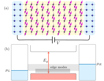
Here we consider the voltage-induced resistance transition in a DE model sandwiched by two electrodes in a capacitor structure shown in Fig. 1(a). The DE system is initially in an insulating meta-stable Néel state with a large band-gap determined by the electron-spin coupling constant. In the presence of an external voltage that is larger than the bandgap , charge carriers at the two electrodes could couple to electron states in the conduction and valance bands of the system. Importantly, due to the delocalized nature of these bulk states, the applied voltage immediately leads to a finite current flow. The bulk of the system quickly becomes unstable and undergoes a fast transformation to a conducting state through a process similar to the dielectric breakdown.
In this work, we instead focus on an insulator-to-metal transition that is induced by a voltage smaller than the band-gap, . As shown in Fig. 1(b), the chemical potentials and of the two electrodes lie within the band gap in this scenario. Due to the energy mismatch, electrons at the two electrodes cannot efficiently couple to the eigen-states in the bulk. The instability, however, starts at the left edge that is connected to the anode with a chemical potential lower than that in the bulk (yet still higher than the valence band edge). Because of the reduced electron density at the edge, anti-parallel spins are unstable against the delocalization of holes through the DE mechanism. The subsequent re-alignment of spins leads to the formation of hole-rich ferromagnetic clusters at the boundary.
The above scenario can also be understood from the energy diagram shown in Fig. 1(b). The coupling to the two electrodes creates a series of energy-states localized at the two edges. As the applied voltage is increased, the chemical potential of the anode is lowered toward the energy levels of the localized modes at the left edge. These edge modes are similar to the band-tail states introduced by disorder. The resultant resonant coupling between electrons at the left electrode and the edge modes leads to an instability toward the formation of a FM layer as electrons are drawn from the sample through the edge modes. The subsequent expansion of the FM domain drives the transformation to the metallic state. Here we perform the NEGF-LLG simulation to provide a quantitative understanding of the above nucleation and growth scenario of insulator-to-metal phase transformation in the single-band DE model.
The rest of the paper is organized as follows. In Sec. II, we discuss the real-space NEGF-LLG method for simulating the adiabatic dynamics of driven DE systems. We next present in Sec. III the simulation results for the voltage-induced insulator-to-metal transition of a square-lattice DE model. A detailed analysis of the phase transformation kinetics and the propagation of metal-insulator interface is discussed in Sec. IV. Finally, we present a summary and outlook in Sec. V.
II NEGF-LLG dynamics for driven double-exchange systems
We consider a two-dimensional capacitor structure, shown in Fig. 1(a), in which the central region is described by a square-lattice DE Hamiltonian:
| (1) |
where denotes nearest-neighbor pairs, is the nearest-neighbor hopping constant, is the on-site Hund’s rule coupling constant between local spin and conduction electron spin . This single-band DE model exhibits several features that are typical of strongly correlated electron systems, such as a filling-controlled insulator to metal transition and electronic phase separation yunoki98 ; dagotto98 ; chattopadhyay01 ; luo21 . The DE model could thus serve as a simple prototype model system to investigate the voltage driven metal-insulator transition in correlated electron materials. Since the DE mechanism is crucial to the CMR effect in manganites dagotto01 ; dagotto_book , our study here also shed light on RS phenomenon observed in lanthanum manganites such as La1-xAxMnO3 (A = Ca, Sr) chen06 ; krisponeit10 ; krisponeit13 ; krisponeit19 .
The semiclassical dynamics of local spins in the DE model is governed by the stochastic LLG equation
| (2) |
where is the local exchange force, is the Gilbert damping coefficient, and denotes the stochastic forces described by Gaussian distribution. For equilibrium electronic state, the exchange force is given by the partial derivative of a potential energy: , where is the energy of the quasi-equilibrium electron liquid brown63 ; antropov97 ; ma11 ; luo21 . For an out-of-equilibrium quantum state , the energy of the system is not a well-defined quantity. However, the force can still be computed using the generalized Hellmann-Feynman theorem diventra00 ; todorov01 ; stamenova05 ; ohe06 , which for the DE model is given by
| (3) |
Here we have introduced the single-particle density matrix . It is worth noting that this electron-induced non-equilibrium force is related to the spin-transfer torque in, e.g. s-d models, and current-induced phenomena such as tunneling magnetoresistance salahuddin06 ; xie17 ; ellis17 ; petrovic18 ; dolui20 .
The square-lattice DE system is connected to a pair of non-interacting leads at the left and right boundaries. Periodic boundary conditions are assumed in the -direction. Moreover, a bath of non-interacting fermions are coupled to every lattice sites. The total Hamiltonian of our system is , where is the DE Hamiltonian in Eq. (1), and the second term describes the electrodes, reservoir degrees of freedom, and their coupling to the DE system:
| (4) |
Here represents non-interacting fermions from the bath ( inside the bulk) or the leads (for on the two open boundaries), is the spin index, and is a continuous quantum number. For example, encodes the band-structure of the two leads.
After integrating out the reservoir fermions in both leads and the bath, the retarded Green’s function matrix for the central region is , where and are the matrix representation of the DE Hamiltonian and dissipation-induced self-energy, respectively, in the site-spin space. The explicit matrix elements are
| (5) |
| (6) |
The resultant level-broadening matrix is diagonal with . For simplicity, we assume flat wide-band spectrum for the reservoirs, which leads to a frequency-independent broadening factor with two different values and . Next, using the Keldysh formula for quasi-steady state, the lesser Green’s function is obtained from the retarded/advanced Green’s functions: , and the lesser self-energy is related to the through dissipation-fluctuation theorem:
| (7) |
Here or depending on whether site- is at the boundaries or in the bulk. The local chemical potential for the bath, and for the two electrodes, where is the applied voltage. The transmission current of this nonequilibrium state is
| (8) |
where is the transmission function, and are the Fermi-Dirac distribution functions.
The density matrix , which is required for the force calculation Eq. (3) in the NEGF-LLG dynamics can now be computed from
| (9) |
for quasi-steady electron state diventra00 ; todorov01 ; stamenova05 ; ohe06 . Here we have explicitly shown the dependence of both the Green’s function and the density matrix on the instantaneous spin configuration . Given the forces acting on spins, a second-order algorithm is used to integrate the stochastic LLG equation. In the following, the energy is measured in units of , while time is measured in .
III nonequilibrium insulator-to-metal transition
We apply the above NEGF-LLG method to simulate the voltage-induced insulator-to-metal transition of the capacitor structure described by . The initial state of our simulations was obtained first using the equilibrium LLG dynamics simulations with half-filled electrons per site. As temperature , this results in a Néel order on the square lattice. The band structure a perfect Néel order is given by , where is the energy dispersion of the square-lattice tight-binding Hamiltonian. Importantly, an energy gap is opened in the spectrum. At half-filling, the valance band is completely filled, and the DE system is in a band-insulator state.
Next we turn on the coupling to the bath at a negative chemical potential , which still lies within the gap; see Fig. 1(b). This coupling can be thought of as a gating-induced doping at high temperatures. Importantly, this half-filled Néel state remains stable as long as is within the band gap and the temperature is low enough . This stability is confirmed by our NEGF-LLG simulations of the Néel state with a reduced chemical potential at and : a thin layer of slightly depleted electrons occurs at each of the two electrodes, while the bulk remains in the half-filled insulating state with almost perfect antiferromagnetic spin order.
In the presence of an external voltage , a chemical potential difference is introduced between the two electrodes. Crucially, the instability that leads to the insulator-to-metal transition is not driven by this potential difference. Since the bulk remains gapped at half-filling, the chemical-potential difference is not large enough to induce a current flow, which could lead to an instability of the bulk through the DE mechanism. Instead, the instability comes from the enhanced coupling between the anode and the in-gap modes localized at the left edge when significantly overlaps with the energy levels of these edge modes; see Fig. 1(b). This resonant coupling between the electrode and the edge modes leads to nucleation of seed ferromagnetic clusters localized at the left boundary.
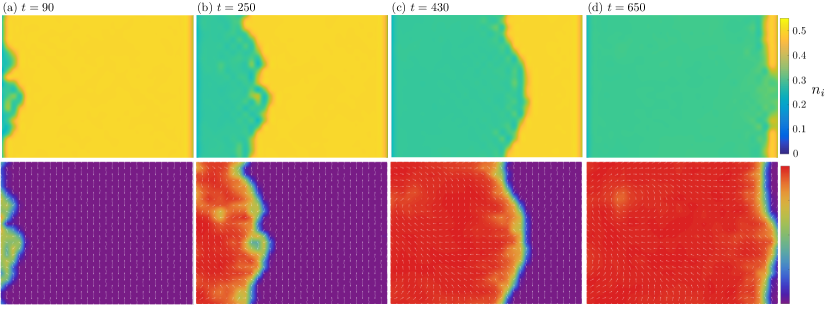
Fig. 2 shows an example of the phase transformation of the driven DE system. The external voltage is turned on at time , giving rise to a chemical potential difference at the two electrodes. Other simulation parameters are: the Hund’s coupling , Gilbert damping coefficient , level-broadening coefficients , , temperature , and the time step . The chemical potential of the bath is set at , and the chemical potentials at the two electrodes are . The top panels show the snapshots of local electron filling fraction at different times of the NEGF-LLG simulations, while the corresponding spin configurations are shown in the bottom panels.
As discussed above, the nonequilibrium phase transformation starts with the nucleation of the FM regions at the left edge as electrons are drained to the anode. As the nuclei merge to form a hole-rich domain, a metal-insulator (MI) interface is created and driven to the right by the voltage stress. Across the MI interface, the electron density changes from on the insulating side to on the metallic side. To characterize the spin configurations, we introduce a nearest-neighbor bond variables , which is insensitive to the global rotations of spins. The bond-variable serves as an indicator for the short-range spin correlations. As expected from the DE mechanism yunoki98 ; dagotto98 ; chattopadhyay01 , FM spin correlation develops in the nucleated hole-rich regions while the insulating domain remains dominated by AFM order; see the bottom panels in Fig. 2.
A more quantitative description of the voltage-driven phase transformation is summarized in Fig. 3 which shows the time dependence of the transmission current , the spatially averaged electron filling fraction , the Néel or AFM order parameter , and the spatial-averaged bond variable . The initial nucleation of the FM clusters is characterized by an incubation timescale . During this period, spins at the left edge gradually realign themselves and form seeds of hole-rich FM clusters. The AFM order parameter and the electron filling only decrease noticeably for .
After the incubation time, a clear metal-insulator (MI) interface is created. During the interval , the resultant MI domain-wall propagates across the bulk of the system. As shown in Fig. 3(a) and (b), the average electron filling fraction decreases almost linearly with time, while the transmission current remains nearly negligible during this period of domain-wall propagation. The expansion of the metallic regions also results in a decrease of the AFM order parameter . The transformation from the AFM to the FM state is also described by the steady increase of the averaged bond-variable from to ; see Fig. 3(c) and (d). As the MI interface reaches the cathode at the opposite end, the FM domain takes over the system, giving rise to a quasi-steady-state regime () characterized by a nonzero transmission current and a low electron filling .
During the propagation of the MI-interface, the system remains insulating and the transmission current is very small. Detailed examination shows that the current increases exponentially in this period. The inset of Fig. 3(a) shows the transmission current in log-scale as a function of time. The exponential growth also indicates that transmission of electrons at this stage is mainly through quantum tunneling. For an insulating AFM domain of linear size , the tunneling current decays exponentially as the distance: , where is a numerical constant. Since the MI-interface propagates with a roughly constant velocity, to be discussed in the following, the thickness of the AFM domain decreases linearly with time , leading to an exponentially increasing transmission .
We also compute the local density of states (DOS) from the imaginary part of the electron lesser Green’s function
| (10) |
The DOS at various layers near the anode (the left electrode with a lower chemical potential ) at the beginning of the phase transition is shown in Fig. 4(a). Also shown for comparison is the bulk-averaged DOS, which exhibits a pronounced spectral gap . In fact, the spectral gap is clearly visible even at the second layer. On the other hand, the leftmost layer (), which couples directly to the electrode, exhibits a broad DOS across the spectrum. This gapless DOS indicates the “metallic” nature of the boundary layer, where the nucleation of the hole-rich FM clusters take places.
The DOS in the quasi-steady state () after the system is transformed into the FM state is shown in Fig. 4(b). One can understand these spectral functions from the band structure of an FM-ordered DE system. Here, the dispersion relation of the square-lattice tight-binding model is split into two spin-polarized bands: , where refers to band with electron spins anti-parallel/parallel to the polarized local moments. A small gap occurs at the origin when the Hund’s coupling is greater than half the original bandwidth. The two bands separated by a small gap at in Fig. 4(b) correspond to the two spin-polarized bands of the FM state, while the two arrows indicate the position of the van Hove singularities of the original square-lattice DOS.
Fig. 4(c) shows the bulk averaged DOS at different times during the phase transformation. As more and more layers become ferromagnetic, the spectral gap of the AFM state is gradually filled up. The DOS is transformed into two bands with quasi-polarized spins in a state with short-range FM correlation. The sharp peaks at the band-edges of the AFM state also gradually evolve into two peaks originating from the van Hove singularities of spin polarized bands of the FM state.
IV Kinetics of phase transformation
Next we turn to the kinetics of the voltage-induced phase transformation. We first consider the propagation dynamics of the metal-insulator (MI) domain walls. To this end, we first compute the electron density profile obtained by averaging over the transverse -direction. An example of the density distribution is shown in the inset of Fig. 5(a). Importantly, the electron density exhibits a sharp discontinuity, which can be used to obtain the position of the MI interface. Fig. 5(a) shows the (normalized) displacement of the MI-interface as a function of time for different driving voltages. Notably, a linear regime characterized by a constant velocity emerges after the incubation time that accounts for the nucleation of the FM domains and the formation of the MI interface. Since quenched disorder is not considered in this work, the motion of the MI-interface is expected to be in the so-called flow regime ferrero21 ; jo09 in which the velocity is proportional to the driving force, . This behavior is confirmed in our simulations except for very large applied voltage; see Fig. 6(a). In the presence of quenched disorder, the propagation of the MI-interface at small voltage is expected to exhibit creep motion and depinning dynamics ferrero21 .
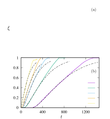
To characterize the early stage of the phase transition and particularly the nucleation of the FM domains, we compute the time-dependent volume fraction of the transformed hole-rich FM phase, which is shown in Fig. 5(b) for varying voltage stresses. These curves are then fitted using the Kolmogorov-Avrami-Ishibashi (KAI) model kolmogorov37 ; avrami40 ; ishibashi71 , which has been widely applied to the domain-wall dynamics of ferroelectric transistors so05 ; gruverman05 ; sharma13 ; kim17 . In the KAI model, the volume fraction of the transformed phase is described by
| (11) |
where is a time scale characterizing the initial domain growth, denotes the incubation time, and is called the Avarami exponent. The inverse timescale extracted from the fitting is shown in Fig. 6(a) as a function of voltage. As expected, the time required to grow the proto-FM domain decreases with increasing driving force.
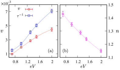
On the other hand, useful information about the growth kinetics is encoded in the Avrami exponent. The original KAI theory predicts that the exponent ishibashi71 , where is the spatial dimension and the parameter for constant nucleation rate, and for pre-existing nuclei. Since nucleation of the FM-domain only takes place at the electrode, the Avrami exponent is expected to be given by the dimension in the square-lattice DE model. Interestingly, we find that our NEGF-LLG simulation results can be well described by the KAI mechanism albeit with a non-integer Avrami exponent that decreases with increasing voltage; see Fig. 6(b). Such fractional effective dimension indicates the nontrivial growth geometry of our system ishibashi71 ; shur98 . One can also understands the voltage dependence as follows. At large voltage stress, the uniform and roughly simultaneous nucleation at the edge of the system results in a unidirectional domain growth and an exponent . On the other hand, the sporadic and non-uniform distribution of the nucleation sites in the case of small voltages give rise to a growth kinetics that preserves some 2D nature of the system as demonstrated in the case of Fig. 2(a).
V Conclusion and outlook
To summarize, we have uncovered surface-induced insulator-to-metal transformation in a double-exchange system driven by an external voltage. The instability of the initial insulating Néel state is triggered by the coupling between the electrode and the in-gap modes that are localized at the sample boundary. Our multi-scale NEGF-LLG simulations show that the phase transformation proceeds via the nucleation of a metallic layer at the anode and the subsequent propagation of the metal-insulator domain-wall through the system. The initial nucleation and growth of the ferromagnetic domains are well described by the KAI model with an effective dimension depending on the voltage stress. The resultant FM-AFM domain wall propagates through the system with an approximately constant velocity, which increases with the driving voltage. At the end of the phase transformation, the driven DE system enters a nonequilibrium quasi-steady state with a nonzero transmission current.
The domain-wall driven transition picture is consistent with the experiments on lanthanum manganites La1-xAxMnO3 with A = Sr or Ca chen06 ; krisponeit10 ; krisponeit13 . A non-volatile and bipolar switching with sharp threshold was observed in, e.g. La0.8Ca0.2MnO3 (LCMO) krisponeit10 . Furthermore, using conductive atomic force microscopy, nanometer-sized conducting regions were identified during the RS. Interestingly, the size of the metallic islands was found to depend logarithmically on the pulse-width of the applied electric field, a result that is consistent with the scenario of domain-wall creep and depinning lemerle98 ; chauve00 . This domain-wall propagation picture is further supported by the noise of the current during RS krisponeit13 , similar to the famous Barkhausen noise in magnetization reversal. It is worth noting that the above picture is different from the ion-migration controlled interface-type RS suggested for another manganite PCMO nian07 . NEGF-LLG simulations for resistance transition in DE systems with quenched disorder will be left for future work.
Another important generalization is the multi-scale modeling of RS dynamics for Hubbard-type interacting models, which is relevant for RS phenomena in several canonical Mott insulators vaju08 ; cario10 ; janod15 ; madan15 ; dubost13 . It is worth noting that complex spin-density wave patterns have been observed in voltage-driven Hubbard model by solving the self-consistent Hartree-Fock equation with NEGF ribeiro16 ; li17 ; dutta20 . However, these works only consider static nonequilibrium solutions of the Hubbard model. A full dynamical modeling of RS phenomena in such systems requires further integration of NEGF-LLG with many-body techniques such as Hartree-Fock method or dynamical mean-field theory. Surrogate many-body solver based on modern machine learning models could be a promising approach for this challenging computational task.
Acknowledgements.
The author thanks A. Ghosh, G. Kotliar, and Jong Han for fruitful discussions. This work is supported by the US Department of Energy Basic Energy Sciences under Contract No. DE-SC0020330. The authors acknowledge Research Computing at The University of Virginia for providing computational resources and technical support that have contributed to the results reported within this work.References
- (1) R. Waser and M. Aono, Nanoionics-based resistive switching memories, Nat. Mater. 6, 833 (2007).
- (2) A. Sawa, Resistive switching in transition metal oxides, Mater. Today 11, 28 (2008).
- (3) R. Waser, R. Dittmann, G. Staikov, K. Szot, Redox-based resistive switching memories - Nanoionic mechanisms, prospects, and challenges, Adv. Mater. 21, 2632 (2009).
- (4) K. M. Kim, D. S. Jeong, and C. S. Hwang, Nanofilamentary resistive switching in binary oxide system; a review on the present status and outlook, Nanotechnology 22, 254002 (2011).
- (5) D. S. Jeong, R. Thomas, R. S. Katiyar, J. F. Scott, H. Kohlstedt, A. Petraru, and C. S. Hwang, Emerging memories: resistive switching mechanisms and current status, Rep. Prog. Phys. 75, 076502 (2012).
- (6) J. S. Lee, S. Lee, and T. W. Noh, Resistive switching phenomena: A review of statistical physics approaches, Appl. Phys. Rev. 2, 031303 (2015).
- (7) W. W. Zhuang, W. Pan, B. D. Ulrich, J. J. Lee, L. Stecker, A. Burmaster, D. R. Evans, S. T. Hsu, M. Tajiri, A. Shimaoka, K. Inoue, T. Naka, N. Awaya, K. Sakiyama, Y. Wang, S. Q. Liu, N. J. Wu, and A. Ignatiev, Novel colossal magnetoresistive thin film nonvolatile resistance random access memory (RRAM), IEEE Int. Electron Devices Meet., Tech. Dig. p.193 (2002).
- (8) I. G. Baek, M. S. Lee, S. Seo, M. J. Lee, D. H. Seo, D. S. Suh, J. C. Park, S. O. Park, H. S. Kim, I. K. Yoo, U. I. Chung, and J. T. Moon, Highly scalable nonvolatile resistive memory using simple binary oxide driven by asymmetric unipolar voltage pulses, IEEE Int. Electron Devices Meet., Tech. Dig. p.587 (2004).
- (9) F. Pan, S. Gao, C. Chen, C. Song, F. Zeng, Recent progress in resistive random access memories: Materials, switching mechanisms, and performance, Mater. Sci. Eng. R Rep. 83, 1 (2014).
- (10) M.-J. Lee, S. Seo, D.-C. Kim, S.-E. Ahn, D. H. Seo, I.-K. Yoo, I.-G. Baek, D.-S. Kim, I.-S. Byun, S.-H. Kim, I.-R. Hwang, J.-S. Kim, S.-H. Jeon, and B. H. Park, A Low-Temperature-Grown Oxide Diode as a New Switch Element for High-Density, Nonvolatile Memories, Adv. Mater. 19, 73 (2007).
- (11) J. Del Valle, J. G. Ramirez, M. J. Rozenberg, and I. K. Schuller, Challenges in materials and devices for resistive-switching-based neuromorphic computing, J. Appl. Phys. 124, 211101 (2018).
- (12) A. A. Fursina, R. G. S. Sofin, I. V. Shvets, and D. Natelson, Origin of hysteresis in resistive switching in magnetite is Joule heating, Phys. Rev. B 79, 245131 (2009).
- (13) Y. B. Nian, J. Strozier, N. J. Wu, X. Chen, and A. Ignatiev, Evidence for an exygen diffusion model for the electric pulse induced resistance change effect in transition-metal oxides, Phys. Rev. Lett. 98, 146403 (2007).
- (14) K. Lee, J.-S. Jang, Y. Kwon, K.-H. Lee, Y.-K. Park, and W. Y. Choi, A unified model for unipolar resistive random access memory, Appl. Phys. Lett. 100, 083509 (2012).
- (15) L. Cario, C. Vaju, B. Corraze, V. Guiot, E. Janod, Electric-Field-Induced Resistive Switching in a Family of Mott Insulators: Towards a New Class of RRAM Memories, Adv. Mater. 22, 5193 (2010).
- (16) N. Onofrio, D. Guzman, and A. Strachan, Atomic origin of ultrafast resistance switching in nanoscale electrometallization cells, Nat. Mater. 14, 440 (2015).
- (17) T. Gergs, S. Dirkmann, and T. Mussenbrock, Integration of external electric fields in molecular dynamics simulation models for resistive switching devices, J. Appl. Phys. 123, 245301 (2018).
- (18) S. Menzel, P. Kaupmann, and W. Rainer, Understanding filamentary growth in electrochemical metallization memory cells using kinetic Monte Carlo simulations, Nanoscale 7, 12673 (2015).
- (19) S. Dirkmann, M. Ziegler, M. Hansen, H. Kohlstedt, J. Trieschmann, and T. Mussenbrock, Kinetic simulation of filament growth dynamics in memristive electrochemical metallization devices, J. Appl. Phys. 118, 214501 (2015).
- (20) S. Dirkmann and T. Mussenbrock, Resistive switching in memristive electrochemical metallization devices, AIP Adv. 7, 065006 (2017).
- (21) X. Guan, S. Yu, H.S.P. Wong, On the switching parameter variation of metal-oxide RRAM? Part I: Physical modeling and simulation methodology. IEEE Trans. Electron Devices. 59, 1172 (2012).
- (22) S. Kim, S.J. Kim, K.M. Kim, S.R. Lee, M. Chang, E. Cho, Y.B. Kim, C.J. Kim, U.I. Chung, I.K. Yoo, Physical electro-thermal model of resistive switching in bi-layered resistance-change memory. Sci. Rep. 3, 1680 (2013).
- (23) J.S. Lee, S.B. Lee, B. Kahng, T.W. Noh, Two opposite hysteresis curves in semiconductors with mobile dopants. Appl. Phys. Lett. 102, 253503 (2013).
- (24) A. Marchewka, B. Roesgen, K. Skaja, H. Du, C.L. Jia, J. Mayer, V. Rana, R. Waser, S. Menzel, Nanoionic resistive switching memories: On the physical nature of the dynamic reset process. Adv. Elec. Mater. 2, 1500233 (2016).
- (25) S. Ambrogio, B. Magyari-Köpe, N. Onofrio, M. M. Islam, D. Duncan, Y. Nishi, and A. Strachan, Modeling resistive switching materials and devices across scales, J. Electroceram. 39, 39 (2017).
- (26) S.C. Chae, J.S. Lee, S. Kim, S.B. Lee, S.H. Chang, C. Liu, B. Kahng, H. Shin, D.W. Kim, C.U. Jung, S. Seo, M.J. Lee, T.W. Noh, Random circuit breaker network model for unipolar resistance switching. Adv. Mater. 20, 1154 (2008).
- (27) S. H. Chang, J. S. Lee, S. C. Chae, S. B. Lee, C. Liu, B. Kahng, D.-W. Kim, and T. W. Noh, Occurrence of Both Unipolar Memory and Threshold Resistance Switching in a NiO Film, Phys. Rev. Lett. 102, 026801 (2009).
- (28) J. S. Lee, S. B. Lee, S. H. Chang, L. G. Gao, B. S. Kang, M.-J. Lee, C. J. Kim, T. W. Noh, and B. Kahng, Scaling Theory for Unipolar Resistance Switching, Phys. Rev. Lett. 105, 205701 (2010).
- (29) X. Chen, N. Wu, J. Strozier, and A. Ignatiev, Spatially extended nature of resistive switching in perovskite oxide thin films, Appl. Phys. Lett. 89, 063507 (2006).
- (30) J.-O. Krisponeit, C. Kalkert, B. Damaschke, V. Moshnyaga, and K. Samwer, Nanoscale resistance switching in manganite thin films: Sharp voltage threshold and pulse-width dependence, Phys. Rev. B 82, 144440 (2010).
- (31) J.-O. Krisponeit, C. Kalkert, B. Damaschke, V. Moshnyaga, and K. Samwer, Time-resolved resistive switching on manganite surfaces: Creep and noise signatures indicate pinning of nanoscale domains, Phys. Rev. B 87, 121103(R) (2013).
- (32) J.-O. Krisponeit, B. Damaschke, V. Moshnyaga, and K. Samwer, Layer-by-Layer resistive switching: Multiscale Functionality due to Electric-Field-Induced Healing of Dead Layers, Phys. Rev. Lett. 122, 136801 (2019).
- (33) C. Vaju, L. Cario, B. Corraze, E. Janod, V. Dubost, T. Cren, D. Roditchev, D. Braithwaite, O. Chauvet, Electric-Pulse-driven Electronic Phase Separation, Insulator-Metal Transition, and Possible Superconductivity in a Mott Insulator, Adv. Mater. 20, 2760 (2008).
- (34) E. Janod, J. Tranchant, B. Corraze, M. Querre, P. Stoliar, M. Rozenberg, T. Cren, D. Roditchev, V. T. Phuoc, M.-P. Besland, and L. Cario, Resistive switching in Mott insula- tors and correlated systems, Adv. Funct. Mater. 25, 6287 (2015).
- (35) H. Madan, M. Jerry, A. Pogrebnyakov, T. Mayer, and S. Datta, Quantitative Mapping of Phase Coexistence in Mott-Peierls Insulator during Electronic and Thermally Driven Phase Transition, ACS Nano 9, 2009 (2015).
- (36) V. Dubost, T. Cren, C. Vaju, L. Cario, B. Corraze, E. Janod, F. Debontridder, and D. Roditchev, Resistive Switching at the Nanoscale in the Mott Insulator Compound GaTa4Se8, Nano Lett. 13, 3648 (2013).
- (37) T. Driscoll, J. Quinn, M. Di Ventra, D. N. Basov, G. Seo, Y.-W. Lee, H.-T. Kim, D. R. Smith, Current oscillation in vanadium oxide: Evidence for electrically triggered percolation avalanches, Phys. Rev. B 86, 094203 (2012).
- (38) P. Stoliar, M. Rozenberg, E. Janod, B. Corraze, J. Tranchant, and L. Cario, Nonthermal and purely electronic resistive switching in a Mott memory, Phys. Rev. B 90, 045146 (2014).
- (39) E. Dagotto, T. Hotta, A. Moreo, Colossal magnetoresistant materials: The key role of phase separation, Phys. Rep. 344, 1 (2001).
- (40) E. Dagotto, Nanoscale phase separation and colossal magnetoresistance (Berlin, Springer 2002).
- (41) C. S. Zener, Interaction between the -Shells in the Transition Metals. II. Ferromagnetic Compounds of Manganese with Perovskite Structure, Phys. Rev. 82, 403 (1951).
- (42) P. W. Anderson and H. Hasegawa, Considerations on Double Exchange, Phys. Rev. 100, 675 (1955).
- (43) P. G. de Gennes, Effects of Double Exchange in Magnetic Crystals, Phys. Rev. 118, 141 (1960).
- (44) Y. Meir and N. S. Wingreen, Landauer formula for the current through an interacting electron region, Phys. Rev. Lett. 68, 2512 (1992).
- (45) A.-P. Jauho, N. S. Wingreen, Y. Meir, Time-dependent transport in interacting and noninteracting resonant-tunneling systems, Phys. Rev. B 50, 5528 (1994).
- (46) S. Datta, Electronic Transport in Mesoscopic Systems (Cambridge University Press, Cambridge, 1995).
- (47) H. Haug and A.-P. Jauho, Quantum Kinetics in Transport and Optics of Semiconductors, Springer Series in Solid-State Sciences 123 (Springer-Verlag, Berlin, 2008).
- (48) M. Di Ventra, Electrical Transport in Nanoscale Systems (Cambridge University Press, Cambridge, 2008).
- (49) M. Di Ventra and S. T. Pantelides, Hellmann-Feynman theorem and the definition of forces in quantum time-dependent and transport problems, Phys. Rev. B 61, 16207 (2000).
- (50) T. N. Todorov, Time-dependent tight-binding, J. Phys.: Condens. Matter 13, 10125 (2001).
- (51) M. Stamenova, S. Sanvito, and T. N. Todorov, Current-driven magnetic rearrangement in spin-polarized point contacts, Phys. Rev. B 72, 134407 (2005).
- (52) J.-i Ohe and B. Kramer, Dynamics of a Domain Wall and Spin-Wave Excitations Driven by a Mesoscopic Current, Phys. Rev. Lett. 96, 027204 (2006).
- (53) S. Yunoki, J. Hu, A. L. Malvezzi, A. Moreo, N. Furukawa, and E. Dagotto, Phase Seperation in Electronic Models for Manganites, Phys. Rev. Lett. 80, 845 (1998).
- (54) E. Dagotto, S. Yunoki, A. L. Malvezzi, A. Moreo, J. Hu, S. Capponi, D. Poilblanc, and N. Furukawa, Ferromagnetic Kondo model for manganites: Phase diagram, charge segregation, and influence of quantum localized spins, Phys. Rev. B 58, 6414 (1998).
- (55) A. Chattopadhyay, A. J. Millis, and S. Das Sarma, phase diagram of the double-exchange model, Phys. Rev. B 64, 012416 (2001).
- (56) J. Luo and G.-W. Chern, Dynamics of electronically phase-separated states in the double exchange model, Phys. Rev. B 103, 115137 (2021).
- (57) W. F. Brown, Jr., Thermal fluctuations of a single-domain parti- cle, Phys. Rev. 130, 1677 (1963).
- (58) V. P. Antropov, S. V. Tretyakov, and B. N. Harmon, Spin dy- namics in magnets: Quantum effects and numerical simulations, J. Appl. Phys. 81, 3961 (1997).
- (59) P.-W. Ma and S. L. Dudarev, Langevin spin dynamics, Phys. Rev. B 83, 134418 (2011).
- (60) S. Salahuddin and S. Datta, Self-consistent simulation of quantum transport and magnetization dynamics in spin-torque based devices, Appl. Phys. Lett. 89, 153504 (2006).
- (61) Y. Xie, J. Ma, S. Ganguly, and A. W. Ghosh, From materials to systems: a multiscale analysis of nanomagnetic switching, J. Comput. Electron. 16, 1201 (2017).
- (62) M. O. A. Ellis, M. Stamenova, and S. Sanvito, Multiscale modeling of current-induced switching in magnetic tunnel junctions using ab initio spin-transfer torques, Phys. Rev. B 96, 224410 (2017).
- (63) M. D. Petrović, B. S. Popescu, U. Bajpai, P. Plechac, and B. K. Nikolić, Spin and Charge Pumping by a Steady or Pulse-Current-Driven Magnetic Domain Wall: A Self-Consistent Multiscale Time-Dependent Quantum-Classical Hybrid Approach, Phys. Rev. Appl. 10, 054038 (2018).
- (64) K. Dolui, M. D. Petrović, K. Zollner, P. Plechác, J. Fabian, and B. K. Nikolić, Proximity Spin-Orbit Torque on a Two-Dimensional Magnet within van der Walls Heterostructure: Current-Driven Antiferromagnet-to-Ferromagnet Reversible Nonequilibrium Phase Transition in BIlayer CrI3, Nano Lett. 20, 2288 (2020).
- (65) E. E. Ferrero, L. Foini, T. Giamarchi, A. B. Kolton, A. Rosso, Creep Motion of Elastic Interfaces Driven in a Disordered Landscape, Annu. Rev. Condens. Matter Phys. 12, 111 (2021)
- (66) J. Y. Jo, S. M. Yang, T. H. Kim, H. N. Lee, J.-G. Yoon, S. Park, Y. Jo, M. H. Jung, and T. W. Noh, Nonlinear Dynamics of Domain-Wall Propagation in Epitaxial Ferroelectric Thin Films, Phys. Rev. Lett. 102, 045701 (2009)
- (67) A. N. Kolmogorov, On the Statistical Theory of Crystallization of Metals, Izv. Akad. Nauk, Ser. Math. 3, 355 (1937).
- (68) M. Avrami, Kinetics of Phase Change. I General Theory, J. Chem. Phys. 7, 1103 (1939); II Transformation‐Time Relations for Random Distribution of Nuclei, J. Chem. Phys. 8, 212 (1940).
- (69) Y. Ishibashi and Y. Takagi, Note on Ferroelectric Domain Switching, J. Phys. Soc. Jpn. 31, 506 (1971).
- (70) Y. W. So, D. J. Kim, T. W. Noh, J.-G. Yoon, and T. K. Song, Polarization switching kinetics of epitaxial Pb(Zr0.4Ti0.6)O3 thin films, Appl. Phys. Lett. 86, 092905 (2005).
- (71) A. Gruverman, B. J. Rodriguez, C. Dehoff, J. D. Waldrep, A. I. Kingon, R. J. Nemanich, and J. S. Cross, Direct studies of domain switching dynamics in thin film ferroelectric capacitors, Appl. Phys. Lett. 87, 082902 (2005).
- (72) P. Sharma, R. G. P. McQuaid, L. J. McGilly, J. M. Gregg, and A. Gruverman, Nanoscale Dynamics of Superdomain Boundaries in Single-Crystal BaTiO3 Lamellae, Adv. Mater. 25, 1323 (2013).
- (73) Y. J. Kim, H. W. Park, S. D. Hyun, H. J. Kim, K. D. Kim, Y. H. Lee, T. Moon, Y. B. Lee, M. H. Park, and C. S. Hwang, Voltage Drop in a Ferroelectric Single Layer Capacitor by Retarded Domain Nucleation, Nano Lett. 17, 7796 (2017).
- (74) V. Shur, E. Rumyantsev, and S. Makarov, Kinetics of phase transformations in real finite systems: Application to switching in ferroelectrics, J. Appl. Phys. 84, 445 (1998).
- (75) S. Lemerle, J. Ferré, C. Chappert, V. Mathet, T. Giamarchi, and P. Le Doussal, Domain Wall Creep in an Ising Ultrathin Magnetic Film, Phys. Rev. Lett. 80, 849 (1998).
- (76) P. Chauve, T. Giamarchi, and P. Le Doussal, Creep and depinning in disordered media, Phys. Rev. B 62, 6241 (2000).
- (77) P. Ribeiro, A. E. Antipov, and A. N. Rubtsov, Nonequilibrium breakdown of a correlated insulator through pattern formation, Phys. Rev. B 93, 144305 (2016).
- (78) J. Li, C. Aron, G. Kotliar, and J. E. Han, Microscopic theory of resistive switching in ordered insulators: Electronic versus thermal mechanisms, Nano Lett. 17, 2994 (2017).
- (79) A. Dutta and P. Majumdar, Spatial behavior in a Mott insulator near the voltage-driven resistive transition, Phys. Rev. B 101, 245155 (2020).
- (80) L. Berger, Exchange interaction between ferromagnetic domain wall and electric current in very thin metallic films, J. Appl. Phys. 55, 1954 (1984).
- (81) S. Zhang and Z. Li, Roles of Nonequilibrium Conduction Electrons on the Magnetization Dynamics of Ferromagnets, Phys. Rev. Lett. 93, 127204 (2004).
- (82) For a review see, e.g. F. Matsukura, Y. Tokura, and H. Ohno, Control of magnetism by electric fields, Nat. Nanotechnol. 10, 209 (2015).