Reconcile the Bulk Metallic and Surface Insulating
State in 1T-TaSe2
Abstract
The origin of different electronic states of 1T-TaS2 and 1T-TaSe2 remains controversial due to the complicated correlated electronic properties. We apply scanning tunneling microscopy to study the electronic state of bulk 1T-TaSe2. Both insulating and metallic states are identified in different areas of the same sample. The insulating state is similar to that in 1T-TaS2, concerning both the spectrum and the orbital texture. With detailed investigations in single-step areas, the electronic state measured on the upper-layer surface is found to be associated with differnt stacking orders and the lower layer’s electronic state. The insulating state is most possibly a single-layer property, perturbed to a metallic state by particular stacking orders. Both the metallic and large-gap insulating spectra, together with their corresponding stacking orders, are stable states in 1T-TaSe2. The connected metallic areas lead to the metallic transport behavior. We then reconcile the bulk metallic and surface insulating state in 1T-TaSe2. The rich phenomenon in 1T-TaSe2 deepens our understanding of the correlated electronic state in bulk 1T-TaSe2 and 1T-TaS2.
I Introduction
Layered transition metal dichalcogenides (TMDs) 1T-TaS2 and 1T-TaSe2 are two widely-studied charge density wave (CDW) materials in past few decades [1, 2, 3, 4, 5, 6, 7, 8, 9, 10]. Both materials are at a commensurate CDW (CCDW) phase with a reconstruction at low temperature. A single unpaired electron exists in each star of David (SD), the basic element of the CCDW super-lattice, resulting in a half-filled system. The electron-electron correlation can split the half-filled band to the lower and upper Hubbard band (LHB and UHB) with an insulating gap, called the Mott insulator [11]. In the bulk 1T-TaS2, different experimental techniques confirm the insulating gap around the Fermi level, consistent with the transport result in 1T-TaS2 [5, 6, 7]. The insulating gap nature of 1T-TaS2 is still under debate [12, 13, 14, 15, 16, 17, 18, 19, 20, 21], and is comprehensively studied in our other work [22].
For the bulk 1T-TaSe2, electronic state measured with different techniques are more complicated [23, 24, 25, 26]. Both scanning tunneling microscopy (STM) and angle-resolved photoemission spectroscopy (ARPES) have detected an insulating state on the exposed surface [25, 26]. However, the resistivity measurement shows a metallic behavior in the CCDW phase, also referred to as a bulk metallic state. The bulk metallic state and the surface insulating state have to be reconciled in the same material, which is still far from a complete understanding. On the other hand, Se atoms in 1T-TaSe2 share the same valence as S atoms in 1T-TaS2 [27, 28]. Whether the surface insulating state in 1T-TaSe2 is similar to the correlation-induced state in 1T-TaS2 needs to be clarified. The insulating state in the single-layer film of 1T-TaSe2/TaS2, grown by molecular beam epitaxy (MBE), makes the problem more complicated and fascinating [29, 30].
Here we perform a detailed STM experiment to explore the electronic state of pristine 1T-TaSe2 at low temperature. We find both metallic and insulating states frequently on the exposed surface of 1T-TaSe2. The insulating spectrum in 1T-TaSe2 is very similar to that in 1T-TaS2, from the spectrum to the spatial orbital texture. With multi-step cleaved surfaces, we measure and obtain three different types of spectra, including the large-gap, small-gap, and metallic spectra. The discrepancy of different electronic states in 1T-TaSe2 is found to be associated with different stacking orders.
To infer the intrinsic stacking-order results in the bulk material, we focus on the flat single-step area and extend the measurement to areas away from the step edge. Both the large-gap insulating state and the metallic state are found to be a bulk property, while the small-gap spectrum only exists within a small area around the step edge. When the lower layer is metallic or insulating, we conclude the correspondence between the stacking order and the upper-layer electronic state, and list the number of occurrences of different situations. With the large-gap insulating state most possibly the single-layer property of 1T-TaSe2, the metallic state could originate from the stacking-order-induced interlayer coupling and perturbation to the insulating state. The frequent appearance of metallic state in 1T-TaSe2 leads to the macroscopic metallic transport results. The main difference between 1T-TaS2 and 1T-TaSe2 is that this perturbed metallic state is energetically stable in 1T-TaSe2 but not stable in 1T-TaS2. It requires a further theoretical study to explore how the stacking order induces this perturbation and the different stability of this metallic state in two materials.
II Experiment and Results
High-quality single crystal 1T-TaSe2 was grown with the iodine transport agent. In the STM experiment, 1T-TaSe2 were cleaved in situ in an ultra-high vacuum chamber (base pressure mBar) at liquid nitrogen temperature and transferred to the STM head immediately. Topographies in this paper were collected with a bias voltage mV and setpoint current pA at liquid nitrogen temperature ( K). The differential conductance spectra were acquired by the standard lock-in technique, with a voltage modulation of mV at Hz frequency.
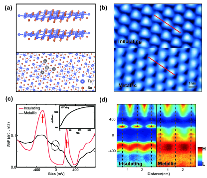
Bulk single crystal 1T-TaSe2 has a CdI2-type layered structure [upper panel of Fig. 1(a)]. In each unit structure, the Ta atomic layer is sandwiched between two Se atomic layers, and the Ta atoms form a triangular lattice in the plane. In the CCDW phase, every Ta atoms are regrouped into a cluster called star-of-David (SD), and the SDs form an enlarged triangular super-lattice [lower panel in Fig. 1(a)]. The center and nearest Ta atoms are labeled by A and B respectively, while the inequivalent next nearest Ta atoms are labeled by C, and C’. The electronic state is strongly modified by the CCDW phase. The bands from Ta atoms are folded into three sub-bands with two filled and one half-filled [23]. In the bulk 1T-TaS2, the half-filled band is split into the LHB and UHB with a Mott insulating gap, consistent with the insulating state in the resistivity measurement. In contrast, the resistivity measurement of 1T-TaSe2 [Fig. 1(c) inset] shows a metallic state at low temperature [1, 2, 3]. The discrepancy of resistivity results of 1T-TaS2 and 1T-TaSe2 has been explained by the different -derived valence bands of S and Se [32, 31, 33, 34, 35]. However, previous ARPES and STM experiment of bulk 1T-TaSe2 also observed that a surface metallic to Mott insulating phase transition occurs when the temperature is reduced to 260 K [25, 26]. The reason for the coexistence of bulk metallic and surface insulating state remains unresolved in 1T-TaSe2.
In our STM experiment, the measurement temperature ( K) is far below the CCDW transition temperature. Insulating and metallic spectra both exist in different areas of each sample we measured. Figure 1(b) are two representative topographies with different electronic states. They share the same triangular SD super-lattice array, with each bright spot corresponding to one SD. Figure 1(c) shows the typical insulating and metallic spectra measured at the center of one SD. The insulating spectrum is very similar to the Mott insulating spectrum measured in bulk 1T-TaS2. The LHB and UHB peaks are located at and mV. The gap size is around mV, about 100 mV larger than that of bulk 1T-TaS2 [35, 36, 37]. The CDW valley roughly at mV shows an approximate zero value, suggesting a strong CDW modulation in 1T-TaSe2 [28]. The metallic spectrum displays a rough linear decay of density-of-state (DOS) around the Fermi energy (zero bias). A weak dip feature appears around the zero bias. The deep valley at mV coincides with the CDW valley in the insulating spectrum.
To show the spatial homogeneity, we present the linecut maps for both the insulating and metallic states. In Fig. 1(d), the horizontal axis is the position along the two red lines crossing three SDs in Fig. 1(b), and the vertical axis is the STM bias ranging from to mV. For the insulating spectra, the LHB and UHB peaks are evident at SD centers, resulting in a periodic intensity variation along the line. The CDW feature above 400 mV also shows an apparent periodic variation, but with maximum peaks shifting by half the period. This phenomenon is similar to that in 1T-TaS2 [35, 36]. The Hubbard bands originate from the central Ta orbital, with LHB and UHB peaks showing maximum values at SD centers. The CDW bands are from the surrounding Ta orbital, with CDW peaks showing maximum values at SD rims. In the linecut map of metallic spectra, the zero-bias dip also shows a periodic variation, and the maximum values are located at SD centers. We expect that the two peaks of the zero-bias dip in the metallic spectrum are also related to the central Ta orbital.
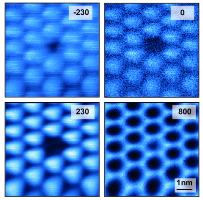
Figure 2 displays the differential conductance maps at several selected energies for a nm2 area with insulating state. A special point defect exists at one SD in the middle of the frame, which is identified to a central Ta vacancy in 1T-TaS2 [22]. The maps reveal more spatial characteristics than the linecut map crossing SDs. With the bias voltage at mV and mV, these two maps are close to the LHB and UHB, respectively. Both maps display a triangular lattice pattern with the bright spots positioned at SD centers, consistent with that the Hubbard band mainly originates from the central Ta orbital. When moving to the lower energy or higher energy, the maps reveal a honeycomb orbital texture (e.g. in the map at mV), consistent with that the CDW bands are from the surrounding Ta orbitals. The energy-dependent orbital texture for the insulating state is similar to that in the bulk 1T-TaS2 [35]. The single-layer MBE-grown 1T-TaSe2 shows a slightly different energy-dependent orbital texture despite of the similar insulating spectrum [29, 30]. The similar insulating spectra in the single-layer and bulk samples suggest that the insulating state is most likely an intrinsic single-layer property.
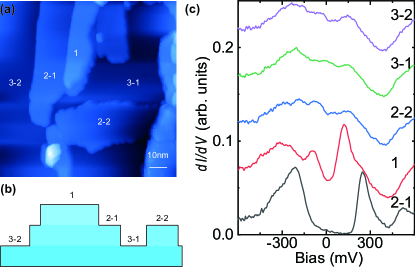
The reason for the different electronic states in different regions is still a mystery. Stacking order has been taken into account in some recent research works [12, 13, 14, 15, 16, 17, 18, 19, 20, 21]. In our other work [22], stacking order has been detailed studied in 1T-TaS2. We apply a similar procedure to study the step areas on cleaved bulk 1T-TaSe2 [22]. Figure 3(a) shows a special large area topography with multi-step environment, taken on the exposed surface of 1T-TaSe2. A schematic side view of this multi-step area is shown in Fig. 3(b), which is derived from the height profiles in topography. As shown in Fig. 3(c), the spectra measured on different step planes exhibits different electronic states.
For the area in Fig. 3(a), the spectrum on the bottom layer (region 3-1 and region 3-2) is a metallic one similar to that in Fig. 1(c). On top of this layer, the spectra exhibit different electronic state, insulating in region 2-1, and metallic in region 2-2. Different electronic states in the same plane (region 2-1 and 2-2) imply different stacking orders exist between the same two layers. Furthermore, the spectrum on region 1 has a reduced gap with peaks at and mV. Although the zero-bias conductance of this type of spectrum is enhanced to a significant value, the curve shape is consistent with the small gap spectrum in 1T-TaS2 [22]. This phenomenon reminds us the similar three types of spectra in the stacking order study in 1T-TaS2 [22].

To study the stacking order, we focus on the flat single-step area which renders a determination of the relative displacement of SD super-lattices in the upper and lower layers. The method is similar to that in our other work [22]. The single-step area also enables us to extend the measurement away from the step edge to check whether the result is more related to the bulk property. In multiple experiments, we only occasionally observe the small-gap spectrum, which also exsits within a small area around the step edge or in a small island area [Fig. 3(a)]. Then we mainly concentrate attention on the large-gap and metallic spectra, which are more related to the intrinsic property of the bulk material. For the following shown examples, they are selected from multiple measurements on different samples.
We first consider the situation with a metallic spectrum on the lower layer. Figure 4(a) and 4(b) show two single-step area topographies, which include triangular SD super-lattices in both the lower layer and the bright upper layer. The spectra measured on the lower and upper layers are shown in Fig. 4(c) and 4(d). On the upper layer, the electronic state shows a metallic spectrum in Fig. 4(c). The metallic spectra of the two layers are basically the same with slight difference near the Fermi level. The corresponding stacking order is the AC-stacking, which means that the SD center of the upper layer is vertically aligned with the outer-corner site of SD in the underlying layer as shown in Fig. 4(e). The metallic-metallic steps are frequently observed during our experiments. Another commonly observed case is the insulating upper layer observed with AA-stacking [Fig.4(d) and 4(f)]. It is worth to mention that although the small-gap spectrum is rarely observed above the metallic layer, the corresponding stacking order is the AB-stacking. Up to our current experiments, the surface electronic states above a metallic layer all shows a one-to-one correspondence with stacking orders.
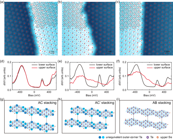
We further consider the situation with an insulating spectrum on the lower layer. The insulating-insulating steps, which are most frequently observed in 1T-TaS2 are also commonly seen in 1T-TaSe2. Different from 1T-TaS2, the AA-stacking of insulating-insulating step only occasionally appears in 1T-TaSe2. The dominate stacking order is the AC-stacking [Fig. 5(a), 5(d), and 5(g)]. Figure 5(b) and 5(c) show two single-step area topographies, with the metallic spectra measured on the upper layers [Fig. 5(e) and 5(f)]. After carefully determining the relative shift of SD super-lattices, the metallic layer in Fig. 5(b) corresponds to the AC’-stacking, which is unequivalent with the AC-stacking in Fig. 5(a). Figure 5(c) corresponds to the AB-stacking order. With multiple measurements, we find that these three cases are all frequent and constantly reproducible.
|
|
stacking order | number | ||||
|---|---|---|---|---|---|---|---|
| metallic | metallic | AC | 6 | ||||
| large-gap insulating | AA | 4 | |||||
| large-gap insulating | large-gap insulating | AC | 7 | ||||
| AA | 1 | ||||||
| metallic | AC’ | 5 | |||||
| AB | 5 |
All different stacking orders and corresponding electronic state of upper and lower layers are summarized in Table 1. As the table shows, the stacking order shows one-to-one correspondence with the upper-layer electronic state, when the lower layer is metallic. When the lower layer is insulating, two different stacking orders can lead to the same upper-layer electronic state. A similar case has happened in 1T-TaS2 [22], in which both AA and AC-stacking lead to the insulating-insulating step. Considering the single-layer property of the large-gap spectrum, both AA and AC-stacking may lead to a negligible interlayer coupling. In contrast, the AC’ and AC-stacking result in a similar perturbed and metallic upper-layer spectrum. The upper-layer spectrum is not only related to the stacking order, but also to the spectrum of the lower layer. The AC-stacking order could correspond to a metalic spectrum in Fig. 4(a) but an insulating spectrum in Fig. 5(a).
There are long-standing puzzles about the insulating state in bulk 1T-TaS2 and 1T-TaSe2. According to the first-principle calculation, there is a conducting band along the direction, which leads to a metallic state near the Fermi level. However, the large insulating gap near the Fermi level has been identified by different experimental methods. Recently, some experiments reveal possible double-layer stacking in 1T-TaS2, which conjures to a band insulator scenario [18, 19, 20]. In our comprehensive results, the AC-stacking in Fig 5(a) corresponds to two large-gap spectra on both the upper and lower terraces, which dispels that the large gap is from the unit-cell doubling of two AA-stacked layers [18, 19, 20]. In fact, different stacking orders appear randomly in our samples. The upper-layer electronic state is determined by the stacking orders and the electronic state of adjacent underlying layer. The large-gap spectrum is most possibly the intrinsic property of a single-layer 1T-TaSe2, similar to that of MBE grown film of 1T-TaSe2. The metallic spectrum is not intrinsic in the single-layer 1T-TaSe2, but a modulated spectrum induced by particular stacking orders.
The metallic spectrum in 1T-TaSe2 shows a rough linear DOS near the Fermi level, different from the V-shaped metallic spectrum in 1T-TaS2. The difference is possibly related to the different valence band of S and Se. The Se atom valence band has a higher energy level than that of S atom, making it easier for the band to hybridize with the band of Ta atoms. On top of the insulating layer, a metallic layer can be induced by the AC’-stacking and AB-stacking orders. Above the metallic layer, the AC-stacking leads to the metallic upper-layer state. When the electron correlation is disturbed, the strong charge transfer between Ta and Se atoms is possibly dominant, leading to the linear DOS decay near the Fermi level. The difference between Se and S bands may also make the metallic perturbed state more stable in terms of energy, while the theoretical explaination is beyond our current capability and needs further investigations.
In 1T-TaSe2, both the metallic and large-gap insulating states can extend all the way at the step edge, although only the large-gap spectrum can extend all the way in 1T-TaS2. The difference is consistent with that both insulating state and metallic state can appear at different regions in the same sample in 1T-TaSe2, while only the insulating state dominates in 1T-TaS2. Please note that although we can only measure the spectrum on exposed terraced areas, the collected information helps to predict the electronic state layer-by-layer when we know the state of underlying layer and the stacking order.
III Conclusion
Combining all above information, we demonstrate that the stacking order plays a crucial role in determining the electronic state in bulk 1T-TaSe2. The main difference between bulk 1T-TaS2 and 1T-TaSe2 is that, the large-gap insulating spectrum dominates in 1T-TaS2. In contrast, many different stacking orders can induce both insulating and metallic states depending on the electronic states of the underlying layer in 1T-TaSe2. A large enough ratio of metallic state can always yield a metallic state in the macroscopic transport measurement.
In pristine 1T-TaSe2, the large-gap insulating state mainly reflects the intrinsic single-layer Mott gap, while some spectral details like the nonzero conductance around the Fermi energy and the slope from LHB to zero bias position may be related to the inter-layer effect along the -axis. In general, the inter-layer coupling plays a stronger role in 1T-TaSe2 than in 1T-TaS2. The extremely easy modulation of the electronic state can also make the MBE film slightly different from the insulating state in bulk sample, possibly related to the substrate-induced effect or the particular growth condition. The Mott physics in TMD materials 1T-TaSe2 and 1T-TaS2 is proved to be exceptionally rich and deserves further exploration.
Acknowledgements.
This work was supported by the National Key Research and Development Program of China (Grants No. 2019YFA0308602), the Key Research and Development Program of Zhejiang Province, China (2021C01002), and the Fundamental Research Funds for the Central Universities in China. Z.L. thanks the National Nature Science Foundation of China (NSFC-11774196) and Tsinghua University Initiative Scientific Research Program. J.J.G., X.L., and Y.P.S. thank the support of the National Key Research and Development Program of China (Grants No. 2016YFA0300404), the National Nature Science Foundation of China (NSFC-11674326 and NSFC-11874357), the Joint Funds of the National Natural Science Foundation of China, and the Chinese Academy of Sciences’ Large-Scale Scientific Facility (U1832141, U1932217, U2032215).References
- [1] J. A. Wilson, F. J. Di Salvo, and S. Mahajan, Charge-Density Waves and Superlattices in the Metallic Layered Transition Metal Dichalcogenides, Adv. Phys. 24, 117 (1975).
- [2] F. J. Di Salvo, J. A. Wilson, B. G. Bagley, and J. V. Waszczak, Effects of Doping on Charge-Density Waves in Layer Compounds, Phys. Rev. B 12, 2220 (1975).
- [3] P. Fazekas and E. Tosatti, Electrical, Structural and Magnetic Properties of Pure and Doped 1T-TaS2, Philos. Mag. B 39, 229 (1979).
- [4] K. Rossnagel, On the Origin of Charge-Density Waves in Select Layered Transition-Metal Dichalcogenides, J. Phys.: Condens. Matter 23, 213001 (2011).
- [5] J. J. Kim, W. Yamaguchi, T. Hasegawa, and K. Kitazawa, Observation of Mott Localization Gap Using Low Temperature Scanning Tunneling Spectroscopy in Commensurate 1T-TaS2, Phys. Rev. Lett. 73, 2103 (1994).
- [6] J. J. Kim, I. Ekvall, and H. Olin, Temperature-Dependent Scanning Tunneling Spectroscopy of 1T-TaS2, Phys. Rev. B 54, 2244 (1996).
- [7] N. V. Smith, S. D. Kevan, and F. J. DiSalvo, Band Structures of the Layer Compounds 1T-TaS2 and 1H-TaSe2 in the Presence of Commensurate Charge-Density Waves, J. Phys. C: Solid State Phys. 18, 3175 (1985).
- [8] B. Sipos, A. F. Kusmartseva, A. Akrap, H. Berger, L. Forró, and E. Tutiš, From Mott State to Superconductivity in 1T-TaS2, Nat. Mater. 7, 960 (2008).
- [9] I. Lutsyk, M. Rogala, P. Dabrowski, P. Krukowski, P. J. Kowalczyk, A. Busiakiewicz, D. A. Kowalczyk, E. Lacinska, J. Binder, N. Olszowska, M. Kopciuszynski, K. Szalowski, M. Gmitra, R. Stepniewski, M. Jalochowski, J. J. Kolodziej, A. Wysmolek, and Z. Klusek, Electronic Structure of Commensurate, Nearly Commensurate, and Incommensurate Phases of 1T-TaS2 by Angle-Resolved Photoelectron Spectroscopy, Scanning Tunneling Spectroscopy, and Density Functional Theory, Phys. Rev. B 98, 195425 (2018).
- [10] E. Lahoud, O. N. Meetei, K. B. Chaska, A. Kanigel, and N. Trivedi, Emergence of a Novel Pseudogap Metallic State in a Disordered 2D Mott Insulator, Phys. Rev. Lett. 112, 206402 (2014).
- [11] N. F. Mott, Metal-Insulator Transition, Rev. Mod. Phys. 40, 677 (1968).
- [12] T. Ritschel, J. Trinckauf, K. Koepernik, B. Bchner, M. v. Zimmermann, H. Berger, Y. I. Joe, P. Abbamonteand, and J. Geck, Orbital Textures and Charge Density Waves in Transition Metal Dichalcogenides, Nat. Phys. 11, 328 (2015).
- [13] T. Ritschel, H. Berger, and J. Geck, Stacking-Driven Gap Formation in Layered 1T-TaS2, Phys. Rev. B, 98, 195134 (2018).
- [14] S. H. Lee, J. S. Goh, and D. Cho, Origin of the Insulating Phase and First-Order Metal-Insulator Transition in 1T-TaS2, Phys. Rev. Lett. 122, 106404 (2019).
- [15] D. B. Shin, T. -D. Nicolas, J. Zhang, M. S. Okyay, A. Rubio, and N. Park, Identification of the Mott Insulating Charge Density Wave State in 1T-TaS2, Phys. Rev. Lett. 126, 196406 (2021).
- [16] L. Ma, C. Ye, Y. Yu, X. F. Lu, X. Niu, S. Kim, D. Feng, D. Tománek, Y. W. Son, X. H. Chen, and Y. B. Zhang, A Metallic Mosaic Phase and the Origin of Mott-Insulating State in 1T-TaS2, Nat. Commun. 7, 10956 (2016).
- [17] D. Cho, S. Cheon, K. S. Kim, S. H. Lee, Y. H. Cho, S. W. Cheong, and H. W. Yeom, Nanoscale Manipulation of the Mott Insulating State Coupled to Charge Order in 1T-TaS2, Nat. Commun. 7, 10453 (2016).
- [18] C. J. Butler, M. Yoshida, T. Hanaguri, and Y. Iwasa, Mottness versus Unit-Cell Doubling as the Driver of the Insulating State in 1T-TaS2, Nat. Commun. 11, 2477 (2020).
- [19] C. J. Butler, M. Yoshida, T. Hanaguri, and Y. Iwasa, Doublonlike Excitations and Their Phononic Coupling in a Mott Charge-Density-Wave System, Phys. Rev. X 11, 011059 (2021).
- [20] J. Lee, K.-H. Jin, H. W. Yeom, Distinguishing a Mott Insulator from a Trivial Insulator with Atomic Adsorbates, Phys. Rev. Lett. 126, 196405 (2021).
- [21] Y. D. Wang, W. L. Yao, Z. M. Xin, T. T. Han, Z. G. Wang, L. Chen, C. Cai, Y. Li, and Y. Zhang, Band Insulator to Mott Insulator Transition in 1T-TaS2, Nat. Commun. 11, 4215 (2020).
- [22] Z. Wu, K. Bu, W. Zhang, Y. Fei, Y. Zheng, J. Gao, X. Luo, Z. Liu, Y.-P. Sun, and Y. Yin, Effect of Stacking Order on the Electronic State of 1T-TaS2, Phys. Rev. B 105, 035109 (2022)
- [23] K. Horiba, K. Ono, J. H. Oh, T. Kihara, S. Nakazono, M. Oshima, O. Shiino, H. W. Yeom, A. Kakizaki, and Y. Aiura, Charge-Density Wave and Three-Dimensional Fermi Surface in 1T-TaSe2 Studied by Photoemission Spectroscopy, Phys. Rev. B 66, 073106 (2002)
- [24] J. J. Kim, W. Yamaguchi, T. Hasegawa, and K. Kitazawa, Site-Specified Tunneling Spectroscopy of Local Sensity of States in the Charge-Density-Wave State of 1T-TaSe2 at 77 K, Phys. Rev. B 50, 4958(R) (1994).
- [25] L. Perfetti, A. Georges, S. Florens, S. Biermann, S. Mitrovic, H. Berger, Y. Tomm, H. Hchst, and M. Grioni, Spectroscopic Signatures of a Bandwidth-Controlled Mott Transition at the Surface of 1T-TaSe2, Phys. Rev. Lett. 90, 166401 (2003).
- [26] S. Colonna, F. Ronci, A. Cricenti, L. Perfetti, H. Berger, and M. Grioni, Mott Phase at the Surface of 1T-TaSe2 Observed by Scanning Tunneling Microscopy, Phys. Rev. Lett. 94, 036405 (2005).
- [27] P. Darancet, A. J. Millis, and C. A. Marianetti, Three-Dimensional Metallic and Two-Dimensional Insulating Behavior in Octahedral Tantalum Dichalcogenides, Phys. Rev. B 90, 045134 (2014).
- [28] Y. Z. Ge and A. Y. Liu, First-Principles Investigation of the Charge-Density-Wave Instability in 1T-TaSe2, Phys. Rev. B 82, 155133 (2010).
- [29] Y. Chen, W. Ruan, M. Wu, S. Tang, H. Ryu, H. Z. Tsai, R. Lee, S. Kahn, F. Liou, C. Jia,Oliver R. Albertini, H. Xiong, Tao Jia, Z. Liu, J. A. Sobota, A. Y. Liu, J. E. Moore, Z. X. Shen, S. G. Louie, S. K. Mo, and M. F. Crommie, Strong Correlations and Orbital Texture in Single-Layer 1T-TaSe2, Nat. Phys. 16, 218 (2020).
- [30] H. Lin, W. Huang, K. Zhao, S. Qiao, Z. Liu, J. Wu, X. Chen, and S. H. Ji, Scanning Tunneling Spectroscopic Study of Monolayer 1T-TaS2 and 1T-TaSe2, Nano Res. 13, 133 (2020).
- [31] F. Clerc, M. Bovet, H. Berger, L. Despont, C. Koitzsch, O. Gallus, L. Patthey, M. Shi, J. Krempasky, M. G. Garnier, and P. Aebi, Spin-Orbit Splitting in the Valence Bands of 1T-TaS2 and 1T-TaSe2, J. Phys. Condens. Matter 16, 3271 (2004).
- [32] M. Bovet, D. Popović, F. Clerc, C. Koitzsch, U. Probst, E. Bucher, H. Berger, D. Naumović, and P. Aebi, Pseudogapped Fermi Surfaces of 1T-TaS2 and 1T-TaSe2: A Charge Density Wave Effect, Phys. Rev. B 69, 125117 (2004).
- [33] Y. Liu, R. Ang, W. J. Lu, W. H. Song, L. J. Li, and Y. P. Sun, Superconductivity Induced by Se-Doping in Layered Charge-Density-Wave System 1T-TaS2-xSex, Appl. Phys. Lett. 102, 192602 (2013)
- [34] R. Ang, Y. Miyata, E. Ieki, K. Nakayama, T. Sato, Y. Liu, W. J. Lu, Y. P. Sun, and T. Takahashi, Superconductivity and Bandwidth-Controlled Mott Metal-Insulator Transition in 1T-TaS2-xSex, Phys. Rev. B 90, 166401 (2003)
- [35] S. Qiao, X. T. Li, N. Z. Wang, W. Ruan, C. Ye, P. Cai, Z. Q. Hao, H. Yao, X. H. Chen, J. Wu, Y. Y. Wang, and Z. Liu, Mottness Collapse in 1T-TaS2-xSex Transition-Metal Dichalcogenide: An Interplay between Localized and Itinerant Orbitals, Phys. Rev. X 7, 041054 (2017).
- [36] D. Cho, Y. H. Cho, S. W. Cheong, K. S. Kim, and H. W. Yeom, Interplay of Electron-Electron and Electron-Phonon Interactions in the Low-Temperature Phase of 1T-TaS2, Phys. Rev. B 92, 085132 (2015).
- [37] K. L. Bu, W. H. Zhang, Y. Fei, Z. X. Wu, Y. Zheng, J. J. Gao, X. Luo, Y. P. Sun, and Y. Yin, Possible Strain Induced Mott Gap Collapse in 1T-TaS2, Commun. Phys. 2, 146 (2019).