Ultrafast charge-transfer dynamics in twisted MoS2/WSe2 heterostructures
Abstract
Two-dimensional transition metal dichalcogenides (TMD) offer a unique platform for creating van-der-Waals heterojunctions with fascinating physical properties and promising applications in optoelectronics and valleytronics. Because of their typical type-II band alignment, photoexcited electrons and holes can separate via interfacial charge transfer. To understand the nature and the dynamics of this charge transfer is of utmost importance for the design and efficiency of potential devices. However, systematic studies concerning the influence of the stacking angle on the charge transfer remain sparse. Here, we apply time- and polarization resolved second-harmonic imaging microscopy to investigate the charge-transfer dynamics for three MoS2/WSe2 heterostructures with different stacking angles at a previously unattainable time-resolution of 6 fs. For 1.70 eV excitation energy, electron transfer from WSe2 to MoS2 is found to depend considerably on the stacking angle with the fastest transfer time observed to be as short as 12 fs. At 1.85 eV excitation energy, ultrafast hole transfer from MoS2 to hybridized states at the -point or to the K-points of WSe2 has to be considered. Surprisingly, the corresponding decay dynamics show only a minor stacking-angle dependence indicating that radiative recombination of indirect -K excitons becomes the dominant decay route for all samples.
Keywords: time-resolved second-harmonic generation, transition metal dichalcogenides, ultrafast charge transfer, heterostructure, pump-probe experiment, nonlinear optical spectroscopy, stacking angle
1 Introduction
Two-dimensional van-der-Waals materials offer a plethora of opportunities for the design and investigation of stacked heterostructures (HS) 1, 2. In particular, heterostructures of transition metal dichalcogenides (TMD) have revealed fascinating properties stimulating fundamental and applied research in the field of optoelectronics and valleytronics 3, 4. Many combinations of different TMD layers form type-II heterojunctions 5 which enables efficient charge separation and results in spatially separated electron-hole pairs following an optical excitation (so called charge-transfer or interlayer excitons) 6, 7, 8, 9, 10, 11, 12, 13, 14, 15, 16, 17. Due to their van-der-Waals coupled nature, structures with arbitrary stacking angles can be designed and manufactured. The relative orientation of the TMDs in turn influences the coupling between the layers and therefore charge transfer, recombination and other properties of the interlayer excitons 18, 19, 20, 11, 21, 22, 23, 24. However, recent experimental studies investigating the influence of the stacking on the ultrafast charge transfer obtained surprisingly diverse results. For MoS2/WSe2 heterostructures, charge transfer has been reported to be faster than the experimental time resolution of 40 fs independent of the examined stacking angles 25. In contrast, much slower charge transfer times of a few hundred femtoseconds and a significant increase for larger rotational mismatch were observed for WS2/WSe2 26.
Thus, the underlying mechanism for the charge transfer process for different van-der-Waals heterostructures still remains elusive and there are several unresolved questions concerning the influence of the stacking configuration on the ultrafast interlayer charge transfer. We have recently shown the capabilities of the experimental method of time- and polarization-resolved second-harmonic (SH) imaging microscopy giving us direct access to the directional ultrafast charge transfer in a rotationally mismatched WSe2/MoSe2 heterostructure 8. In particular, our technique allows for pump-probe experiments in m-sized regions of heterostructures with a time-resolution not accessible in previous studies. Here, we employ this new approach to examine the charge-carrier dynamics in MoS2/WSe2 heterostructures with different stacking angles. The three MoS2/WSe2 samples studied in the present work had been examined beforehand in a systematic study by Kunstmann et al. 11. There it has been conclusively shown that for all stacking configurations photoluminescence from momentum-space indirect -K interlayer excitons is visible after optical excitation with 532 nm (2.33 eV) photons. It is therefore established that for excitation energies significantly exceeding the respective band gaps interlayer charge transfer occurs and that at least some of the excited charge carriers recombine radiatively via a -K transition. Recently, also momentum-space direct K-K photoluminescence at 1.0 eV has been observed for well-aligned MoS2/WSe2 heterostructures 27. In the present study, we want to elucidate the corresponding ultrafast dynamics in dependence of the stacking angle for three selected stacking angles: 9° (referred to as quasi-3R), 52° (quasi-2H) and 16° (misaligned).
2 Results and Discussion
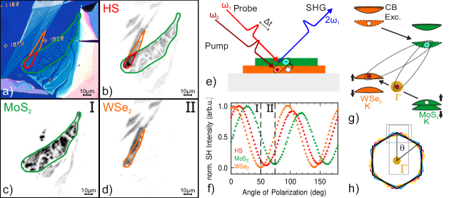
Our method of choice is polarization- and time-resolved second-harmonic imaging microscopy. By careful selection of the polarization angle of the 800-nm (1.55 eV) probe light, we are able to extract changes in the nonlinear susceptibility of individual monolayers inside the TMD heterostructures. For TMD monolayers, the pump-induced changes of the SH response upon resonant optical excitation of intralayer excitons have been shown to be closely correlated to the observed exciton dynamics in linear optical spectroscopy 28. In case of TMD heterostructures, our pump-probe experiments schematically sketched in Fig. 1(e) allow us to access the dynamics of interlayer charge transfer 8. The three studied MoS2/WSe2 samples were mechanically exfoliated and transferred onto a SiO2/Si(001) substrate as described in Ref. 11. Figs. 1(a)-(d) compare an optical microscopy image of one of the studied samples with respective images obtained for different probe polarizations with our SH imaging microscopy. Due to the inherent structural sensitivity of second-harmonic generation (SHG), we are able to directly identify the different monolayer regions and their overlap to determine the position of the heterostructure.
Fig. 1(f) displays the normalized SH response in dependence of the polarization of the probe laser evaluated for the monolayer and heterostructure regions. From these measurements the crystal orientations in relation to the lab coordinates can be determined. The probe polarization for our time-resolved measurements is then chosen to maximize the sensitivity for the MoS2 layer by fully suppressing the SH contribution of WSe2 (polarization I). For 1.70 eV pump-photon energy intralayer A-excitons of WSe2 are resonantly excited 29, 30. Fig. 2(a) shows the corresponding SH-transients of the heterostructures selectively detected by probing the ultrafast nonlinear response of the MoS2 layer in direct comparison with the respective transients obtained from the individual monolayers. All SH transients have been normalized to the signal at negative delays. As expected the MoS2 monolayer transient (filled black data) shows no pump-induced change since the excitation energy is below its A-exciton resonance. In contrast, the SH-intensity of the MoS2 layers of the heterostructures exhibits a clear modulation as a function of the pump-probe delay time. We observe a rapid decrease and a subsequent slower recovery. Since any direct excitation of the MoS2 can be excluded from the monolayer results, we can therefore assign the observed dynamics in the heterostructures to ultrafast electron transfer to MoS2 after optical excitation of WSe2 as sketched in Fig. 2(c). This attribution is also corroborated by the delayed onset of the heterostructure signals in relation to the WSe2 monolayer response and by the ongoing/delayed decrease of the SH intensity, which extends even beyond the duration of the pump pulse (cf. dashed line, CCR).
While there is clear evidence for charge transfer in all heterostructure samples, the observed ultrafast dynamics differ considerably for the three different stackings. Apparently, the fastest electron transfer can be found for the quasi-2H stacked sample (blue data), followed by the quasi-3R (red data) and the misaligned sample (yellow data). This is confirmed quantitatively by a rate-equation model consisting of coupled differential equations in which one energetically higher lying state is filled by a gaussian pump pulse and then subsequently populates the lower lying state with a transfer time . The extracted transfer times for the quasi-3R and the misaligned sample are comparable with values of 6510 fs and 8410 fs, respectively, whereas the transfer time for the quasi-2H stacked sample is more than five times faster (126 fs). This disparity might be surprising since the variation of the lattice separation between the layers, which has a central influence on the tunneling probability 31, is negligible between 2H- and 3R-stacking 11. However, it has also been reported that the wavefunction overlap between the layers plays an important role for the charge transfer across the interface as well as for the subsequent recombination dynamics 19. Accordingly, wavefunction calculations for the interfacial plane in TMD heterostructures have shown strong differences for 3R- and 2H-stacking 32, which then in turn can indeed influence the dynamics 33.
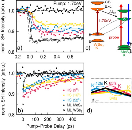
Consequently, we conclude that the faster interlayer electron transfer for the quasi-2H stacked sample is caused by the stronger interlayer interaction of the involved monolayer states at the K-point. In accordance, the observed recombination dynamics shown in Fig. 2(b) also differ significantly for the three heterostructures as determined from a single-exponential fit of the SH transients to extract the individual lifetimes. The misaligned sample shows the longest (46716 ps), the quasi-3R stacked sample an intermediate (30912 ps) and the quasi-2H stacked sample the shortest lifetime (15812 ps). The enhanced lifetime for the misaligned sample could be an indication for the absence of the radiative decay channel as was reported recently27. The difference in lifetime between quasi-2H and quasi-3R can then be explained by the same reasoning as the enhanced transfer. Since the charge transfer via a phonon-assisted tunneling process can be amplified by the spatial overlap of the involved wavefunctions 6, 31, the same should hold for the reversed process of interlayer exciton recombination: A stronger spatial coincidence facilitates the recombination resulting then in a reduced lifetime. Please note, that all three heterostructure lifetimes are considerably extended in comparison to the lifetime observed for the WSe2 monolayer. The latter can be described by a bi-exponential recovery behaviour with much shorter lifetimes of = 3.5 ps and = 30 ps. This enhanced lifetime for the heterostructure signals is in perfect agreement with our interpretation, since the spatially indirect nature of interlayer excitons leads to a strong increase of their lifetimes in comparison to intralayer excitons 34, 15.
In the following, we would like to address open questions concerning the ultrafast hole transfer and the particular influence that hybridized states at the -point have on charge transfer and recombination. In order to elucidate these processes, the pump-photon energy is tuned to 1.85 eV for resonant optical excitation of MoS2 intralayer A-excitons 29, 30. While at this photon energy both materials are excited, the generated exciton density in MoS2 (5.3cm2) is about five times larger than in WSe2 (9.3cm2), as calculated based on energy-dependent absorption of the two layers (see method section). Thus, the pump-induced effects in WSe2 are not negligible, however, the dynamic response measured in MoS2 is mainly dominated by its inherently generated charge carriers. Fig. 3 shows the same time regimes as before using identical colors for the different structures, but now the systems are pumped at 1.85 eV. By comparing the dynamics of Figs. 2(a) and 3(a) striking differences become obvious: First of all, upon 1.85-eV photoexcitation the pump-induced effects now already start to occur precisely at temporal overlap in accordance with a direct excitation in MoS2. With respect to the delayed filling, the SH transients of the quasi-3R and the misaligned sample stay similar, whereas the behaviour of the quasi-2H stacked sample changes drastically. In contrast to the 1.70-eV excitation, where the SH signal of the quasi-2H sample was observed to recover mono-exponentially with a slow recovery rate, the SH response after 1.85-eV excitation begins to recover immediately on a femtosecond timescale. The extracted lifetime is only slightly slower than the corresponding monolayer decay times for 1.85-eV excitation ().
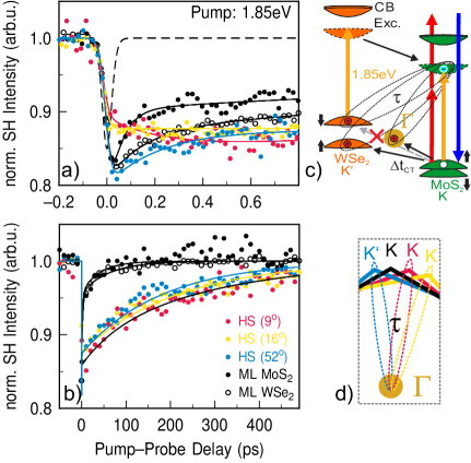
This ultrafast decay process is associated with the coherent radiative recombination of intralayer excitons 35, 36. On the one hand, the slightly slower recovery for the heterostructure signal compared to the monolayer can be explained by the change of the dielectric environment: The enhanced screening for the heterostructure decreases the binding energy of the excitons and therefore increases their Bohr radius and the recombination time. On the other hand, the coherent radiative recombination competes with additional relaxation mechanism in the heterostructure such as hole transfer to the hybridized -point or to the WSe2 layer as illustrated in Fig. 3(c). Since at 1.85-eV excitation electron transfer from the WSe2 into the MoS2 is feasible as well, the detected SH signal in the MoS2 is a mixture of various processes and a clear interpretation of our SH transients becomes more challenging. The competing processes might also explain why we do not observe any clear ultrafast component for the quasi-3R and the misaligned heterostructure sample in our data. Another plausible explanation for the absence of the ultrafast decay in these two heterostructures could also be related to the energy alignment and the spin structure of the involved states. After photoexcitation inside the MoS2 the generated hole has two obvious relaxation pathways alternative to intralayer recombination: it can either be scattered to the hybridized states around the -point or to the K/K’-point in WSe2. In the case of 2H-stacking, transfer to the valence band maximum of WSe2 at K’ is spin forbidden as sketched in Fig. 3(c). For the misaligned sample, scattering to K/K’ should also be reduced due to the large momentum mismatch. In contrast, hole transfer to the valence band maximum at the K-point should be most efficient in case of 3R-stacking. Assuming the hole transfer to K/K’ to be a competing process to the coherent recombination and taking place on a similar or faster timescale, the decreasing efficiency of the hole transfer to K/K’ from quasi-3R, misaligned to quasi-2H could then explain the increasing manifestation of the coherent recombination.
The comparison of the SH transients at large pump-probe delays for both excitation energies in Figs. 2(b) and 3(b) reveals a surprising change in the dynamics caused by the higher excitation energy. For 1.70-eV excitation the recovery rates of the three heterostructure samples differ considerably as discussed above. In the case of 1.85-eV excitation, however, the lifetimes become very similar for all samples (quasi-2H: 1789 ps, quasi-3R: 2178 ps, misaligned: 2197 ps). For 1.70-eV excitation, the quasi-2H configuration showed the fastest recovery time due to the larger wavefunction overlap between the layers. For 1.85 eV, however, the lack of interaction between the layers for the other two samples is compensated by the additional decay routes of the charge carriers generated in the MoS2. The central difference between the two excitation energies is that for 1.85-eV excitation the hole states around the -point become energetically available. Photoluminescence from momentum-space indirect -K interlayer excitons has been observed for all examined stacking configurations of MoS2/WSe2 11. Therefore, we attribute our observed decay dynamics to the radiative recombination of -K interlayer excitons. Due to the fact that the states around the -point consist inherently of orbitals which are delocalized and therefore spread out over both layers the overlap of the wavefunctions of electron and hole is enhanced and, thus, radiative recombination is facilitated. This overall enhancement of the recombination compensates the reduced overlap for the quasi-3R and misaligned sample equalizing the lifetimes of the excitation independent of the stacking configuration.
3 Conclusion
In conclusion, we have employed time- and polarization-resolved second-harmonic imaging microscopy to study the ultrafast charge-carrier dynamics across the MoS2/WSe2 heterostructure interface for different stacking configurations. For lower excitation energies of 1.70 eV, electron transfer from WSe2 to MoS2 is found to depend considerably on the stacking angle and the transfer time is reduced by a factor of seven when going from a larger rotational mismatch towards 2H-stacking. At higher excitation energies, ultrafast hole transfer from MoS2 to hybridized states at the -point and to the K-points of WSe2 has to be considered. The respective decay dynamics, however, does not show a significant dependence on the stacking angle indicating that radiative recombination of indirect -K excitons becomes the dominant decay route for all samples.
4 Methods
The experiments were performed under ambient conditions using a Yb:KGW-based ultrashort pulse laser system (Light Conversion Carbide) feeding two optical parametric amplifiers (Orpheus-F Twin, Orpheus-N) providing photon energies in the range from 1.3-1.9 eV at pulse lengths routinely shorter than 35 fs at a repetition rate of 200 kHz. The photon energy of the probe pulse was chosen to be 1.55 eV well below the bandgap of both materials in order to exclude optical excitation by the probe beam. Our temporal resolution is only limited by the laser system and can be estimated by measurement of the cross-correlation on the sample. The CCR is measured to be 30 fs. The minimal time-resolution is estimated to be 1/5th of the CCR and corresponds to 6 fs. Both beams are focussed collinearly onto the sample under an angle of 18°. After passing a 400-nm dielectric filter, the specular reflected SH response of the probe beam is imaged optically magnified by a camera lens on an electron-multiplied CCD chip (Princeton Instruments ProEM-HS). Typical exposure times are 10 seconds. The applied magnification was M35-40. The overall resolution of our imaging microscopy setup is better than 4 m. The time-delay between pump and probe beam is varied by a motorized delay stage. The polarization of pump and probe beam can be varied by means of /2-plates. The typically detected p-polarization of the second-harmonic light is separated by an analyzer. The applied pump fluence was fixed to 50 J/cm2 for 1.85 eV and 38 J/cm2 for 1.70 eV on the sample (spot diameter 1/e). The applied probe fluence was fixed to 250 J/cm2. These fluences lead to an initial exciton density of 3.651012/cm2 (WSe2) for 1.70 eV and 9.31011/cm2 (WSe2) as well as 5.31012/cm2 (MoS2) for 1.85 eV pump energy (calculated with data from 30 with the tmm package 37). These excitation densities are below the calculated Mott-density 38 ensuring that we are measuring exciton and not plasma dynamics. Long term measurements with these fluences applied did not exhibit any multishot damage. A more detailed description of the setup can be found elsewhere 28. Sample preparation and characterization is described in detail in Ref. 11.
References
- 1 A. K. Geim and I. V. Grigorieva. Van Der Waals Heterostructures. Nature, 499:419–25, 2013.
- 2 H. Lim, S. I. Yoon, G. Kim, A. R. Jang, and H. S. Shin. Stacking of Two-Dimensional Materials in Lateral and Vertical Directions. Chem. Mater., 26:4891–903, 2014.
- 3 K. F. Mak and J. Shan. Photonics and Optoelectronics of 2d Semiconductor Transition Metal Dichalcogenides. Nat. Photonics, 10:216–26, 2016.
- 4 X. D. Xu, W. Yao, D. Xiao, and T. F. Heinz. Spin and Pseudospins in Layered Transition Metal Dichalcogenides. Nat. Phys., 10:343–50, 2014.
- 5 V. O. Özcelik, J. G. Azadani, C. Yang, S. J. Koester, and T. Low. Band alignment of two-dimensional semiconductors for designing heterostructures with momentum space matching. Phys. Rev. B, 94:035125, 2016.
- 6 Z. Wang, P. Altmann, C. Gadermaier, Y. Yang, W. Li, L. Ghirardini, C. Trovatello, M. Finazzi, L. Duò, M. Celebrano, R. Long, D. Akinwande, O. V. Prezhdo, G. Cerullo, and C. S. Dal. Phonon-Mediated Interlayer Charge Separation and Recombination in a MoSe2/WSe2 Heterostructure. Nano Letters, 21:2165–2173, 2021.
- 7 S.-W. Zheng, H.-Y. Wang, L. Wang, H. Wang, and H.-B. Sun. Layer-Dependent Electron Transfer and Recombination Processes in MoS2/WSe2 Multilayer Heterostructures. The Journal of Physical Chemistry Letters, 11(22):9649–9655, 2020.
- 8 J. E. Zimmermann, Y. D. Kim, J. C. Hone., U. Höfer, and G. Mette. Directional ultrafast charge transfer in a WSe2/MoSe2 heterostructure selectively probed by time-resolved SHG imaging microscopy. Nanoscale Horiz., 5:1603–1609, 2020.
- 9 E. V. Calman, L. H. Fowler-Gerace, D. J. Choksy, L. V. Butov, D. E. Nikonov, I. A. Young, S. Hu, A. Mishchenko, and A. K. Geim. Indirect Excitons and Trions in MoSe2/WSe2 Van Der Waals Heterostructures. Nano Lett., 20:1869–75, 2020.
- 10 S. Ovesen, S. Brem, C. Linderalv, M. Kuisma, T. Korn, P. Erhart, M. Selig, and E. Malic. Interlayer Exciton Dynamics in Van Der Waals Heterostructures. Commun. Phys., 2:23, 2019.
- 11 J. Kunstmann, F. Mooshammer, P. Nagler, A. Chaves, F. Stein, N. Paradiso, G. Plechinger, C. Strunk, C. Schüller, G. Seifert, D. R. Reichman, and T. Korn. Momentum-Space Indirect Interlayer Excitons in Transition-Metal Dichalcogenide Van Der Waals Heterostructures. Nat. Phys., 14:801–805, 2018.
- 12 P. Rivera, H. Yu, K. L. Seyler, N. P. Wilson, W. Yao, and X. Xu. Interlayer Valley Excitons in Heterobilayers of Transition Metal Dichalcogenides. Nat. Nanotechnol., 13:1004, 2018.
- 13 B. Miller, A. Steinhoff, B. Pano, J. Klein, F. Jahnke, A. Holleitner, and U. Wurstbauer. Long-Lived Direct and Indirect Interlayer Excitons in Van Der Waals Heterostructures. Nano Lett., 17:5229–37, 2017.
- 14 J. R. Schaibley, P. Rivera, H. Y. Yu, K. L. Seyler, J. Q. Yan, D. G. Mandrus, T. Taniguchi, K. Watanabe, W. Yao, and X. D. Xu. Directional Interlayer Spin-Valley Transfer in Two-Dimensional Heterostructures. Nat. Commun., 7:13747, 2016.
- 15 P. Rivera, J. R. Schaibley, A. M. Jones, J. S. Ross, S. F. Wu, G. Aivazian, P. Klement, K. Seyler, G. Clark, N. J. Ghimire, J. Q. Yan, D. G. Mandrus, W. Yao, and X. D. Xu. Observation of Long-Lived Interlayer Excitons in Monolayer MoSe2-WSe2 Heterostructures. Nat. Commun., 6:6242, 2015.
- 16 H. Fang, C. Battaglia, C. Carraro, S. Nemsak, B. Ozdol, J. S. Kang, H. A. Bechtel, S. B. Desai, F. Kronast, A. A. Unal, G. Conti, C. Conlon, G. K. Palsson, M. C. Martin, A. M. Minor, C. S. Fadley, E. Yablonovitch, R. Maboudian, and A. Javey. Strong Interlayer Coupling in Van Der Waals Heterostructures Built from Single-Layer Chalcogenides. P. Natl. Acad. Sci. USA, 111:6198–202, 2014.
- 17 X. P. Hong, J. Kim, S. F. Shi, Y. Zhang, C. H. Jin, Y. H. Sun, S. Tongay, J. Q. Wu, Y. F. Zhang, and F. Wang. Ultrafast Charge Transfer in Atomically Thin MoS2/WS2 Heterostructures. Nat. Nanotechnol., 9:682–86, 2014.
- 18 M. Brotons-Gisbert, H. Baek, A. Molina-Sánchez, A. Campbell, E. Scerri, D. White, K. Watanabe, T. Taniguchi, C. Bonato, and B. D. Gerardot. Spin–layer locking of interlayer excitons trapped in moiré potentials. Nat. Materials, 19:630–636, 2020.
- 19 P. Merkl, F. Mooshammer, S. Brem, A. Girnghuber, K.-Q. Lin, L. Weigl, M. Liebich, C.-K. Yong, R. Gillen, J. Maultzsch, J. M. Lupton, E. Malic, and R. Huber. Twist-Tailoring Coulomb Correlations in Van Der Waals Homobilayers. Nat. Commun., 11:2167, 2020.
- 20 P. K. Gogoi, Y. C. Lin, R. Senga, H. P. Komsa, S. L. Wong, D. Z. Chi, A. V. Krasheninnikov, L. J. Li, M. B. H. Breese, S. J. Pennycook, A. T. S. Wee, and K. Suenaga. Layer Rotation-Angle-Dependent Excitonic Absorption in Van Der Waals Heterostructures Revealed by Electron Energy Loss Spectroscopy. ACS Nano, 13:9541–50, 2019.
- 21 W.-T. Hsu, L.-S. Lu, P.-H. Wu, M.-H. Lee, P.-J. Chen, P.-Y. Wu, Y.-C. Chou, H.-T. Jeng, L.-J. Li, M.-W. Chu, and W.-H. Chang. Negative Circular Polarization Emissions from WSe2/MoSe2 Commensurate Heterobilayers. Nat. Commun., 9:1356, 2018.
- 22 P. C. Yeh, W. Jin, N. Zaki, J. Kunstmann, D. Chenet, G. Arefe, J. T. Sadowski, J. I. Dadap, P. Sutter, J. Hone, and R. M. Osgood. Direct Measurement of the Tunable Electronic Structure of Bilayer MoS2 by Interlayer Twist. Nano Lett., 16:953–59, 2016.
- 23 S. J. Zheng, L. F. Sun, X. H. Zhou, F. C. Liu, Z. Liu, Z. X. Shen, and H. J. Fan. Coupling and Interlayer Exciton in Twist-Stacked WS2 Bilayers. Adv. Opt. Mater., 3:1600–05, 2015.
- 24 K. H. Liu, L. M. Zhang, T. Cao, C. H. Jin, D. A. Qiu, Q. Zhou, A. Zettl, P. D. Yang, S. G. Louie, and F. Wang. Evolution of Interlayer Coupling in Twisted Molybdenum Disulfide Bilayers. Nat. Commun., 5:4966, 2014.
- 25 H. M. Zhu, J. Wang, Z. Z. Gong, Y. D. Kim, J. Hone, and X. Y. Zhu. Interfacial Charge Transfer Circumventing Momentum Mismatch at Two-Dimensional Van Der Waals Heterojunctions. Nano Lett., 17:3591–98, 2017.
- 26 P. Merkl, F. Mooshammer, P. Steinleitner, A. Girnghuber, K. Q. Lin, P. Nagler, J. Holler, C. Schüller, J. M. Lupton, T. Korn, S. Ovesen, S. Brem, E. Malic, and R. Huber. Ultrafast Transition between Exciton Phases in Van Der Waals Heterostructures. Nat. Mater., 18:691–696, 2019.
- 27 O. Karni, E. Barré, S. C Lau, R. Gillen, E. Y. Ma, B. Kim, K. Watanabe, T. Taniguchi, J. Maultzsch, K. Barmak, R. H. Page, and T. F. Heinz. Infrared Interlayer Exciton Emission in MoS2/WSe2 Heterostructures. Phys. Rev. Lett., 123:247402, 2019.
- 28 J. E. Zimmermann, B. Li, J. C. Hone, U. Höfer, and G. Mette. Second-harmonic imaging microscopy for time-resolved investigations of transition metal dichalcogenides. Journal of Physics: Condensed Matter, 32(48):485901, 2020.
- 29 D. Kozawa, R. Kumar, A. Carvalho, K. K. Amara, W. J. Zhao, S. F. Wang, M. L. Toh, R. M. Ribeiro, A. H. C. Neto, K. Matsuda, and G. Eda. Photocarrier Relaxation Pathway in Two-Dimensional Semiconducting Transition Metal Dichalcogenides. Nat. Commun., 5:4543, 2014.
- 30 Y. L. Li, A. Chernikov, X. Zhang, A. Rigosi, H. M. Hill, A. M. van der Zande, D. A. Chenet, E. M. Shih, J. Hone, and T. F. Heinz. Measurement of the Optical Dielectric Function of Monolayer Transition-Metal Dichalcogenides: MoS2, MoSe2, WS2, and WSe2. Phys. Rev. B, 90:205422, 2014.
- 31 H. Z. Zhou, Y. D. Zhao, W. J. Tao, Y. J. Li, Q. H. Zhou, and H. M. Zhu. Controlling Exciton and Valley Dynamics in Two-Dimensional Heterostructures with Atomically Precise Interlayer Proximity. ACS Nano, 14:4618–25, 2020.
- 32 H. Wang, J. Bang, Y. Sun, L. Liang, D. West, V. Meunier, and S. Zhang. The Role of Collective Motion in the Ultrafast Charge Transfer in Van Der Waals Heterostructures. Nat. Commun., 7:11504, 2016.
- 33 H. Zeng, X. Liu, H. Zhang, and X. Cheng. New theoretical insights into the photoinduced carrier transfer dynamics in WS2/WSe2 van der Waals heterostructures. Phys. Chem. Chem. Phys., 23:694–701, 2021.
- 34 F. Ceballos, M. Z. Bellus, H. Y. Chiu, and H. Zhao. Ultrafast Charge Separation and Indirect Exciton Formation in a MoS2-MoSe2 Van Der Waals Heterostructure. ACS Nano, 8:12717–24, 2014.
- 35 M. Selig, G. Berghäuser, M. Richter, R. Bratschitsch, A. Knorr, and E. Malic. Dark and Bright Exciton Formation, Thermalization, and Photoluminescence in Monolayer Transition Metal Dichalcogenides. 2D Mater., 5:035017, 2018.
- 36 C. Poellmann, P. Steinleitner, U. Leierseder, P. Nagler, G. Plechinger, M. Porer, R. Bratschitsch, C. Schüller, T. Korn, and R. Huber. Resonant Internal Quantum Transitions and Femtosecond Radiative Decay of Excitons in Monolayer WSe2. Nat. Mater., 14:889–893, 2015.
- 37 Steven J. Byrnes. Multilayer optical calculations. arXiv:1603.02720, 2020.
- 38 L. Meckbach, T. Stroucken, and S. W. Koch. Giant Excitation Induced Bandgap Renormalization in TMDC Monolayers. Appl. Phys. Lett., 112:061104, 2018.