First principles studies of the surface and opto-electronic properties of ultra-thin t-Se
Abstract
Selenium is an important earth-abundant and non-toxic semiconductor with numerous applications across the semiconductor industries. Selenium has drawn attention from scientific communities for photovoltaics and imaging devices. Its usage as a photosensitive material largely involves the synthesis of the amorphous phase (a-Se) via various experimental techniques. However, the ground state crystalline phase of this material, known as the trigonal selenium (t-Se), has not been extensively studied for its optimum electronic and optical properties. In this work, we present systematic studies based on density functional theory (DFT) for ultra-thin surface slabs of t-Se. We report the surface energies, work function, electronic and optical properties as a function of number of layers for surface slabs to access its suitability for applications as a photosensitive material.
keywords:
Selenium, ultra-thin-film, surface, DFT, surface energy, work function, optical and electronic properties1 Introduction
Selenium (Se) is a well known photovoltaic material, with its first studies dating back to the late 1800’s [1, 2]. Commonly found in metal sulfide ores [3], Se is an earth-abundant material with a low melting point of C, a relatively simple and stable crystalline structure, and a relatively large direct band-gap [4]. There are a few allotropes of Se, among them the thermodynamically stable triagonal Se (t-Se)111sometimes referred to as hexagonal or crystalline Se. t-Se has been observed to have a large optical absorption coefficient across a wide range of wavelengths. A large absorption coefficient and a low melting point are attractive properties that facilitate the fabrication of large scale amorphous Se (a-Se) photovoltaic devices through vacuum deposition techniques.
Amorphous selenium has been the subject of research firstly for its application in xerographic photocopiers [5, 6], then as a medium for direct X-ray imaging [7, 8, 9, 10], as well as for applications in composite films used in photocells [11, 12, 13]. More recently research into Se’s potential application as a general use photon detector with a potential wide wavelength application from the visible to UV [14, 15]; see [16] for a useful summary.
A new application of Se as a photon detector is foreseen in gas and liquid based noble element particle detectors. Noble element detectors have become ubiquitous in searches for dark matter and as a medium for detection of neutrino-nucleus interactions [17, 18]. The detection of the scintillation light arising from particle interactions is a key component. The scintillation light for the most common noble element detectors (Argon & Xenon) sits in the vacuum ultraviolet (VUV) spectrum (128nm – 175nm) or (9.7 eV – 7.1 eV). Conventional photon detectors such as photo-multiplier tubes (PMT’s) and multi-pixel photon counters (MPPC’s) have diminished quantum efficiency at these wavelengths prompting both alternative detection techniques utilizing wavelength shifting coatings [19] and the development of new VUV sensitive MPPC’s [20]. Each of these approaches comes with their own complications, from the unintended behavior of the wavelength shifters [21, 22] to the small active surface areas of the individual VUV sensitive detectors [23]. In this landscape, techniques utilizing thin films of photosensitive semiconductors offers an opportunity for the development of alternative photon detector designs using new materials, such as a-Se.
Some experimental work measuring the properties of Se based photon detector in the UV spectrum has taken place [24, 25, 9, 14, 15], but little theoretical work modeling and understanding the opto-electronic properties of Se exists for photons in this frequency range. This work serves as a starting point for such calculations to better understand the properties that a selenium based detector might have for photons in the VUV spectrum. We begin with calculations for t-Se modeling ultra-thin films which can be configured as fully relaxed free-standing layers. From these calculations, the surface energies can show the stability of ultra-thin layers of t-Se and the density of states (DOS), band structures, band gaps, and work function. These can illuminate the optoelectronic properties, such as absorption coefficient, reflectivity, refractive index, and electron loss function for Se in the wavelength range most relevant for noble element detectors. In future works, the transition from t-Se to a-Se structures will be enabled by the theoretical calculations presented here.
In this work, we present density functional theory based first principles studies of t-Se surface slabs having up to 15 atomic layers (45 atoms per unit cell). The paper is structured into three sections, the first describes the method of simulation for t-Se (bulk and surface) using density functional theory (DFT) and the details of computational, thermodynamic, and optical modeling. The next section overviews the most important results pertaining to the optoelectronic properties. We conclude by outlining the next phase of the work. A supplemental section is provided at the end to give additional numerical and graphical details where relevant.
2 Methods
The theoretical framework of this work is based on the density functional theory (DFT) [26, 27] implemented with the projector augmented wave method (PAW) [28, 29] as in Vienna ab initio simulation package (VASP) [30, 31]. Even though local magnetic structures are not expected, all the calculations performed in this work with spin polarization to allow additional freedom in electronic relaxations. For crystal structures and slabs visualization, VESTA [32] was used throughout the work.
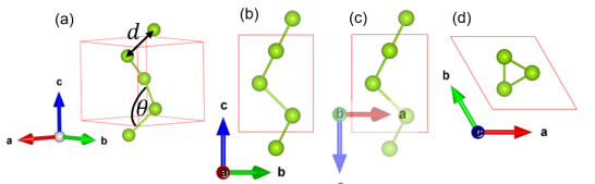
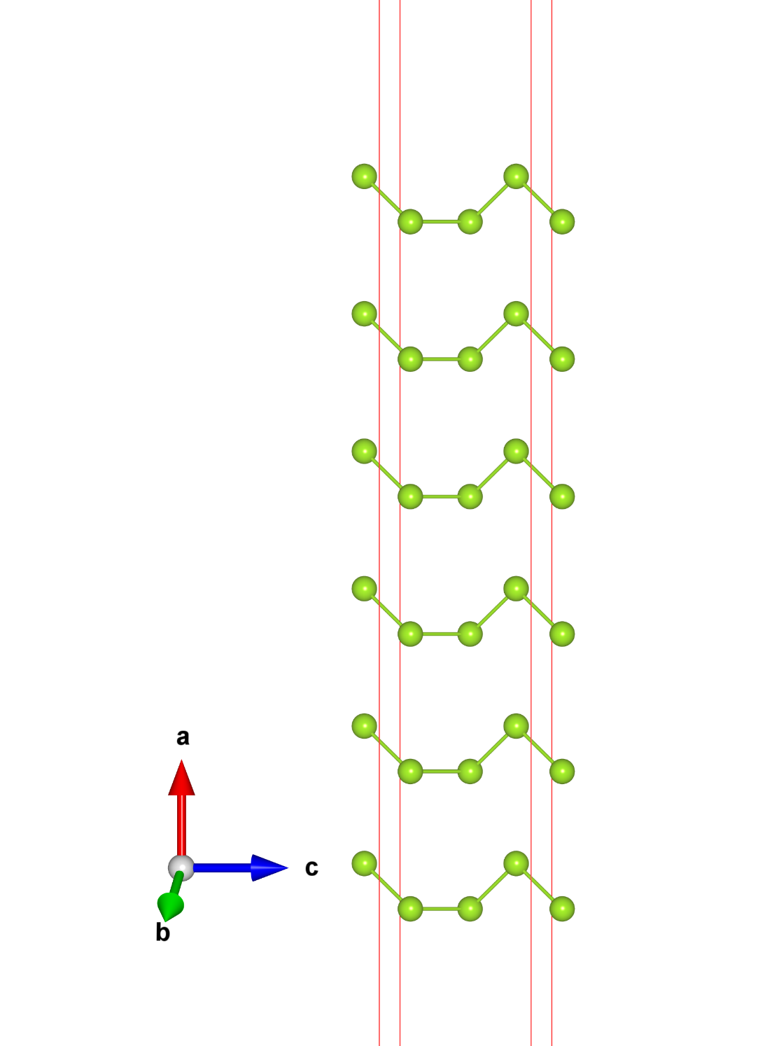
Figure 1 shows the crystal structure of t-Se which contains three selenium atoms per unit cell. Figure 2 shows a typical slab geometry of stacked t-Se used in the calculations.
2.1 Computational Details
In this work, generalized gradient approximation (GGA) functional by Perdew–Burke–Ernserhof (PBE) [33, 34] for the exchange-correlation energy is deployed. Since selenium atoms in t-Se are layered along and directions, as shown in Figure 1, and the inter-layer distance is over 4 Å, we have included van der Waals corrections (vdW) to GGA-DFT through zero damping DFT-D3 method of Grimme [35]. The crystal structure of trigonal selenium with experimental lattice constants and bond lengths [4, 36, 37, 38] and GGA and GGA+vdW optimized lattice parameters are summarized in Tables 1 and 2.
| Lattice parameters for t-Se | ||||||
| a (Å) | b (Å) | c (Å) | ||||
| Experiment [4, 37, 38] | 4.366 | 4.366 | 4.954 | 90 | 90 | 120 |
| GGA | 4.504 | 4.504 | 4.504 | 90 | 90 | 120 |
| GGA + vdW | 4.184 | 4.184 | 5.127 | 90 | 90 | 120 |
| Bond length, d (Å) | Bond angle, | |
|---|---|---|
| Experiment [4, 37, 38] | 2.373 | 103.07 |
| GGA | 2.405 | 103.62 |
| GGA + vdW | 2.431 | 103.98 |
In the analysis of the simulation, we find that the inter-layer separation decreased after van der Waals corrections were applied due to enhanced long-range interactions. In addition, the cohesive energy per atom calculated by GGA + vdW (2.734 ) for bulk t-Se is 0.203 lower than the GGA (2.937 ) computed value. The cohesive energy per atom was calculated using the following formula:
| (1) |
where is the total energy of bulk selenium per unit cell, is the total number of atoms in a unit cell, and is the energy of a single selenium atom in a cubic box of dimension 10 Å. The experimental cohesive energy is 2.25 /atom [39], which indicate that GGA+vdW agrees better with the experimental value compared to the GGA-only calculation of cohesive energy. The binding between the Se atoms in the t-Se crystals is significantly weaker when compared to the binding, for example, of Si (4.62 /atom) [40].
Since selenium atomic layers along and directions are arranged in the same geometric fashion in t-Se crystals, atomic layers from a unit cell were stacked along direction only with a 25 Å vacuum for modeling slabs. A schematic of a six-layers slab oriented in the direction is presented in Figure 2.
All slabs considered in this work for surface properties calculations were geometrically optimized without any symmetry constrained. Atoms in the simulation box could relax in all three lattice directions, and we name these relaxed layers as “free-standing” layers. Throughout the relaxation, cell volumes with vacuum layers (25 Å) were kept fixed. The convergence criteria for the electronic self-consistent loop was set equal to or less than 110-8 eV/Å. All the ions were relaxed until the Hellman-Feynman force was equal to or less than 0.001 Å. The kinetic energy cut off for the plane-wave basis set was 400 eV. Se 4s2 4p4 is the valence electrons configuration considered for this work. Each atomic layer in a (11) slab contains three selenium atoms. In this work, the largest (11) slab contains 15 atomic layers (45 atoms). The Brillouin zone was sampled by a 12121 gamma centered k-mesh for slabs having up to 10 layers (30 atoms) and by a 11515 gamma centered k-mesh for slabs containing more than 10 layers.
2.2 Modeling of Surface Stability
For the characterization of the stability of the surface of t-Se, the surface energy, was calculated using the following formula:
| (2) |
where is the total energy of bulk selenium per unit cell, is the number of layers, is the total energy of -number of layers, and is the surface area.
To avoid inconsistencies in the surface energies, in Eq. (2) resulting from a separate bulk calculation for [41], a well-established method is to derive from a least square fitting of curve by re-writing the Eq. (2) in the form :
| (3) |
The slope in Eq. (3) provides the required to calculate from Eq.(2). This method is tested throughly in previous works [42, 43, 44]. In our case, the fitted values and separate bulk calculations for are very close to one another as summarized in Table 3. In particular, for both GGA and GGA + vdW calculated energies, the difference is within 0.01 eV. Details of the convergence for the surface energies and the least square fitting techniques are given in Figure 4 and section 3.1.
2.3 Modeling of Optical Properties
In order to calculate the optical properties, we calculated the frequency-dependent complex dielectric function in the independent particle picture using VASP. The expression for the real () and imaginary () parts of the dielectric function () as a function of photon frequency () were as in ref.[45]. Using the following formulas, the optical absorption coefficient (, reflectivity (), refractive index ( and the electron energy loss function () were calculated for all the surface slabs and bulk t-Se:
| (4) |
| (5) |
| (6) |
| (7) |
Where the extinction coefficient is defined as
| (8) |
3 Results and Discussion
The results of the simulation are discussed in four subsections. Section 3.1 focuses on the stability analysis and reports the surface energies of surface for t-Se slabs containing up to 15 atomic layers. Section 3.2 shows the calculated work function to further understand the stability of those layers. Section 3.3 reports the calculated electronic properties such as band structures, band gaps and the density of states. Lastly, Section 3.4 presents the calculated optical properties for all the relaxed layers considered in this work. As described above, all the calculations have considered the van der Waals corrections separately, along with GGA-DFT.
3.1 Surface Energies
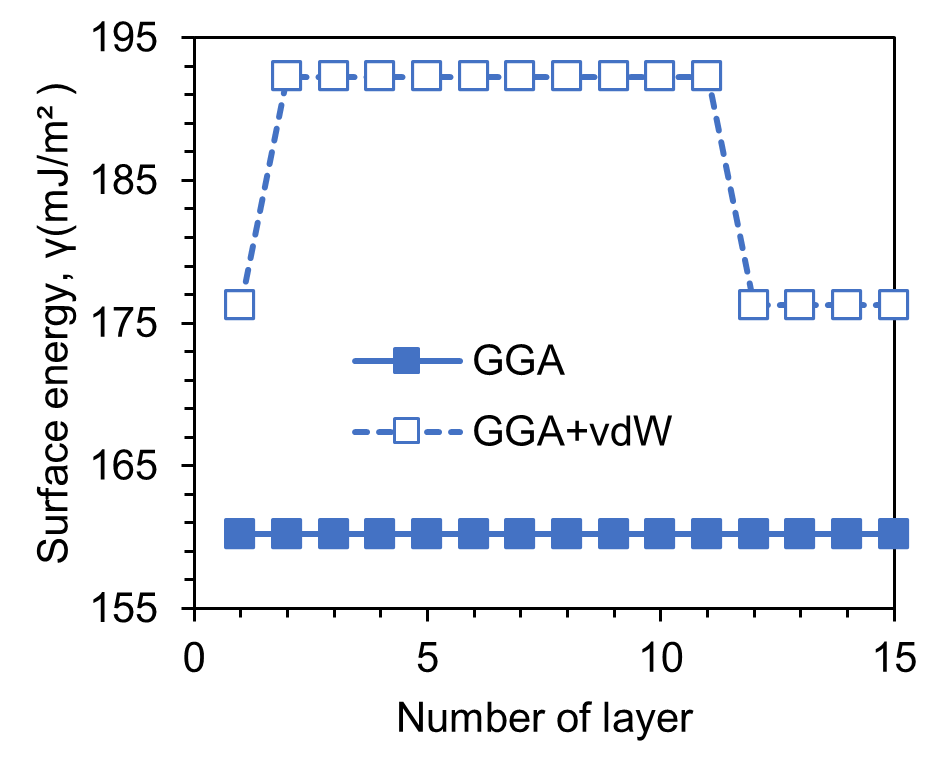
The GGA calculated converged surface energy for free standing t-Se surface slabs is 160.22 . When van der Waals interactions are added, the converged energy becomes approximately 16 higher, which is 176.24 . This increment is expected due to the long-range vdW interaction term added to the Kohn-Sham Hamiltonian. Our calculated values are in reasonably good agreement with experimentally measured surface energies of selenium (175 - 291 ) [46, 47]. The surface energies shown in Figure 3 are calculated values with respect to the number of layers in the slab model; numerical values are presented in Table 5 of Supplemental Material.
As a convergence criteria of surface energies calculation, the incremental energy per formula unit, or atomic layer, was calculated using the following formula
| (9) |
where (for both GGA and GGA + vdW). This is reported as a function of the number of layers, as shown in Figures 4(b).
In addition, the total energies of layers are reported as a function of the number of layers, see Figures 4(c), to obtain the slope from a least square fitting to estimate for the energies of bulk selenium ().
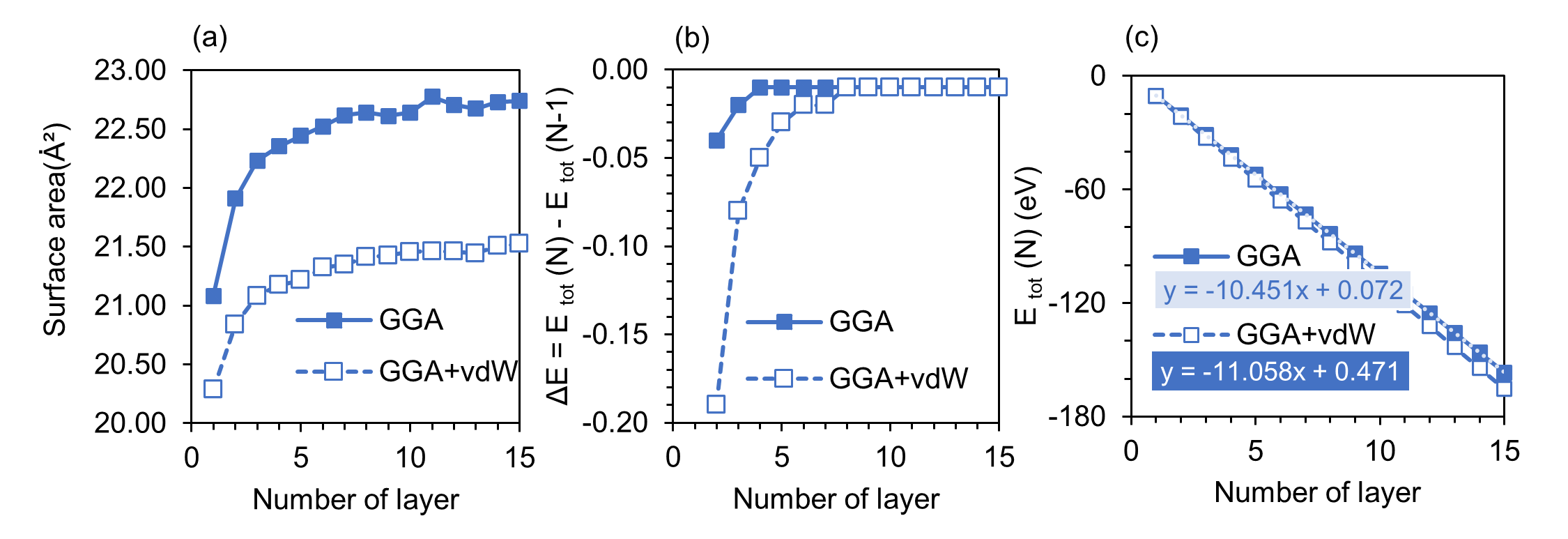
Once is found, was calculated following Equation 2 and were tabulated in Table 5. From Figure 4, the layer-to-layer incremental energy saturates after seven layers for both GGA and GGA+vdW. However, the surface energy does not converge for GGA+vdW till twelve layers; there is a small fall in the value after eleven layers. The fall is due to the combined effect of larger surface area and higher layer-thickness per unit layer as the number of layers increased.
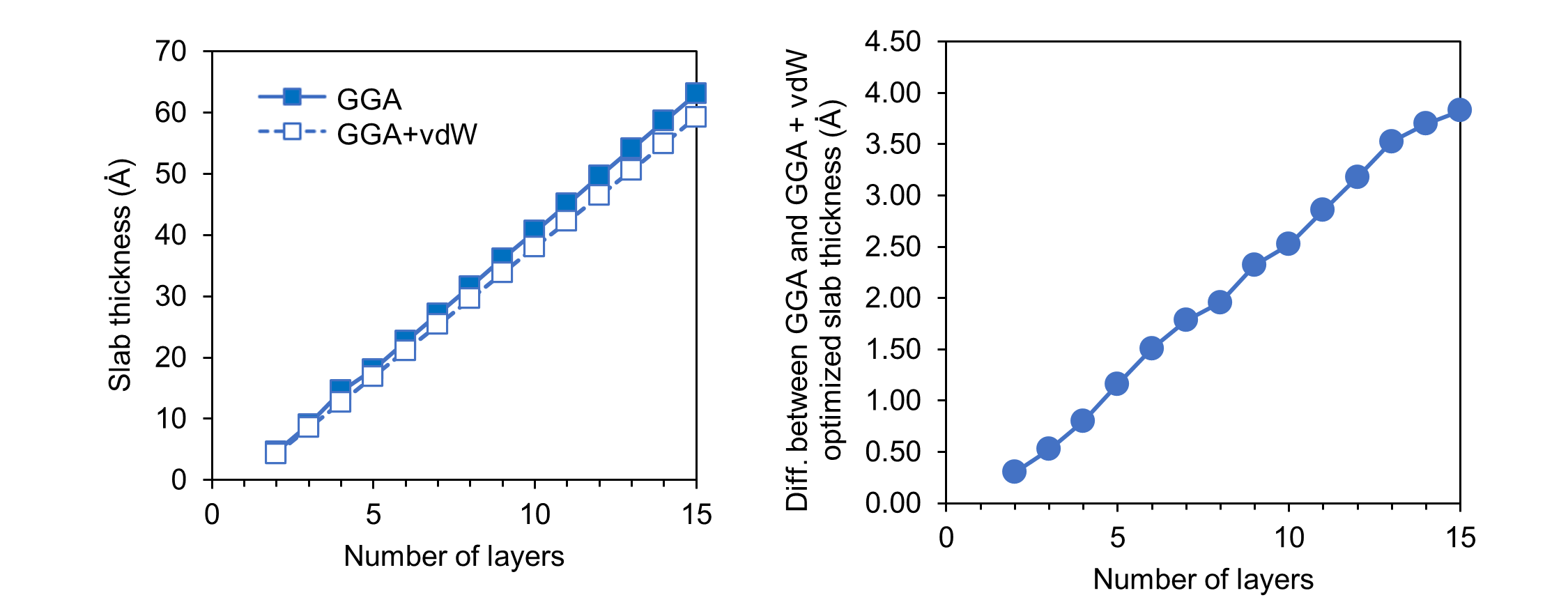
The higher surface energy resulting from GGA + vdW calculations can also be explained from Figure 5 which shows that the rate at which the layer thickness increases with subsequent number of layers is higher for GGA calculated values than the GGA + vdW. This is due to the layer thickness for GGA + vdW-relaxed slabs being less and thus the inter-layer interaction increases, resulting in slightly higher surface energies.
| Total Energy (eV) of t-Se per atomic layer or formula unit | ||
|---|---|---|
| GGA | GGA + vdW | |
| Bulk | -10.450 | -11.059 |
| Least square fitting | -10.451 | -11.058 |
3.2 Work Function
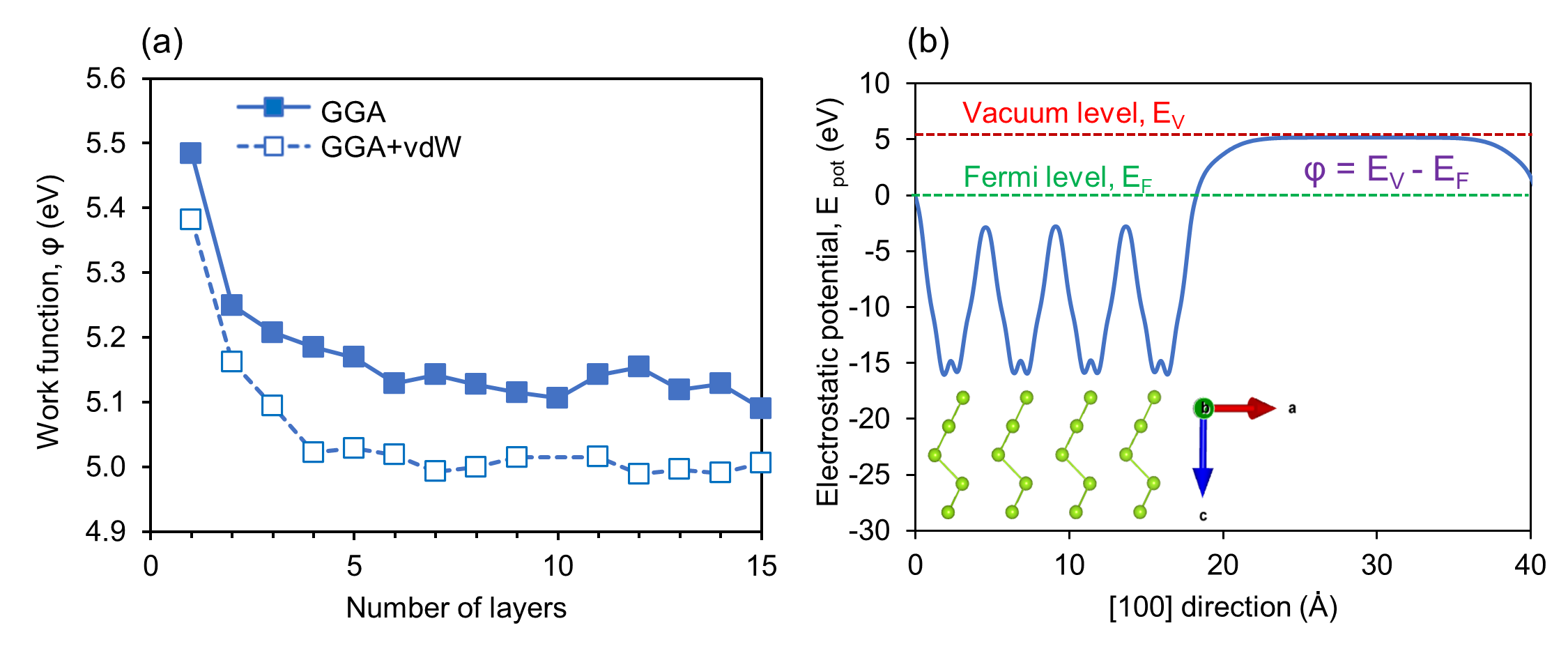
To assess the surface stability further, we have calculated the work function of surface of t-Se. The work function of a semiconductor corresponds to the least amount of energy required to remove an electron from the bulk through the surface so that the electron no longer interacts with the material. It can be calculated as
| (10) |
where is a vacuum level energy, a reference value within the slab model, and is the Fermi level. Within the slab model employed for the present study, the is defined as the saturated electrostatic potential energy as depicted in Figure 6(b). A higher work function indicates a higher stability of a surface, i.e., the surface is less reactive. The calculated work function for surface slabs are presented in Figure 6(a) as a function of the number of layers. A single atomic layer of selenium has the highest work function (5.4 - 5.5 eV). As the number of layers increases, the work function decreases and tends to converge toward 5.1 eV for GGA optimized slabs. For GGA + vdW optimized slabs, this value is slightly lower but comparable to the bulk selenium surface work function (5.11 eV). Since minute changes in the surface configuration can change work function significantly, GGA + vdW optimized layers have lower values than the GGA relaxed layers. However, such higher values of work function for both cases (GGA and GGA+vdW) show good surface stability of the slabs considered for this work. Note, from four atomic layers, free-standing slabs have almost the same work functions as the bulk surface.
3.3 Electronic Properties
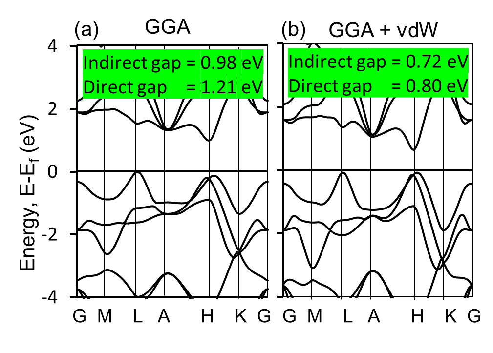
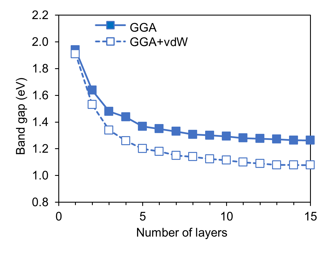
Here the electronic properties of surface t-Se slabs are presented. We begin with the band gap which are calculated through GGA and GGA + vdW formalism. These are shown in Figure 7. We find that the band gap () is the highest for one atomic layer, 1.94 from GGA and 1.91 from GGA+vdW calculations, and much higher than the bulk band gaps (see Figure 15 in Supplemental Material). As the number of layers increases, the band gap decreases and tends to reach the limit of the bulk selenium. The results can be justifies by the quantum confinement effect. Note, the calculated band gaps by either GGA or GGA+vdW method is an underestimation of the experimental band gap of 1.86 eV for t-Se. [39] The underestimation of band gaps is a well-known features by the standard DFT functionals. [48, 49]
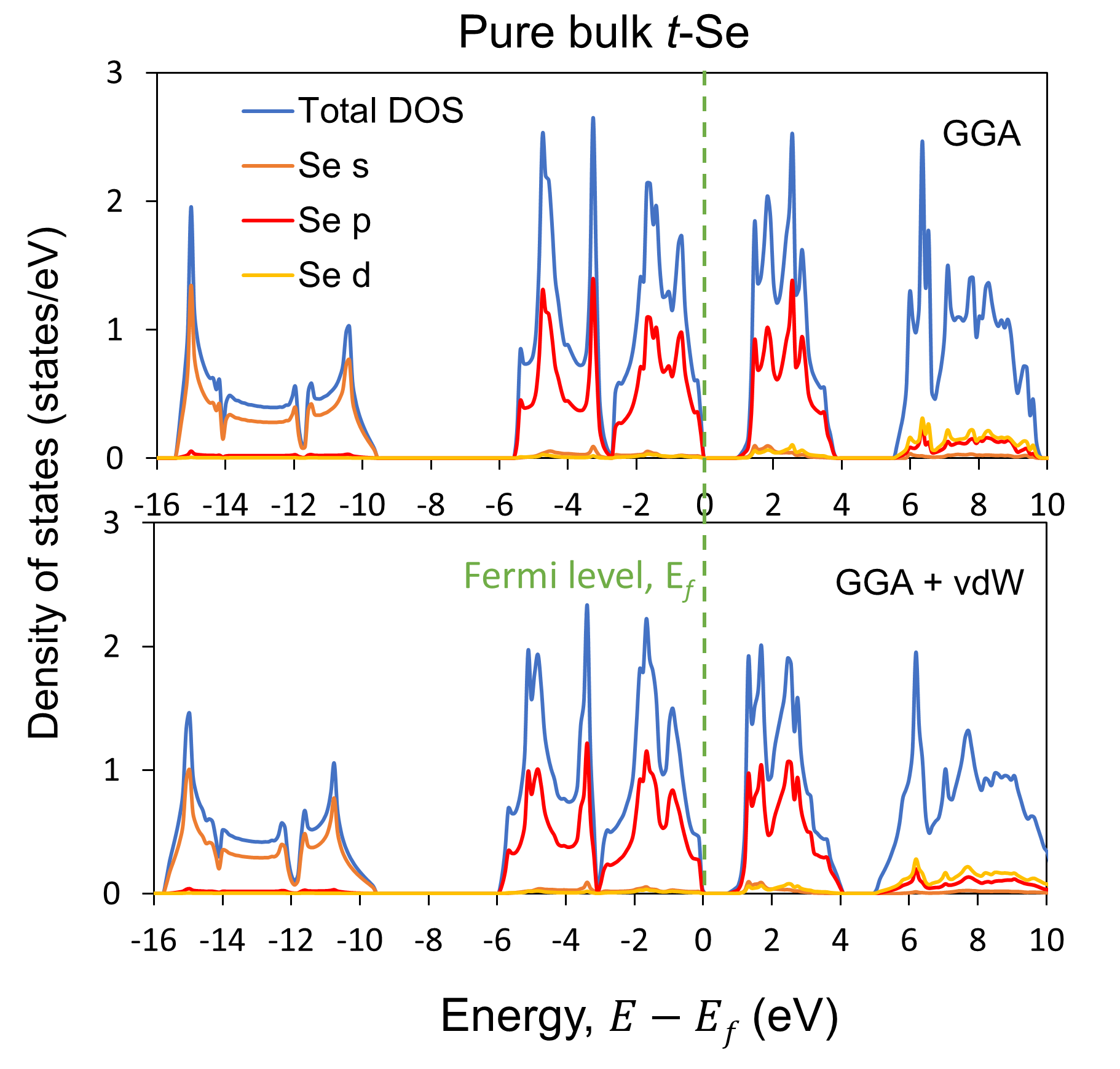
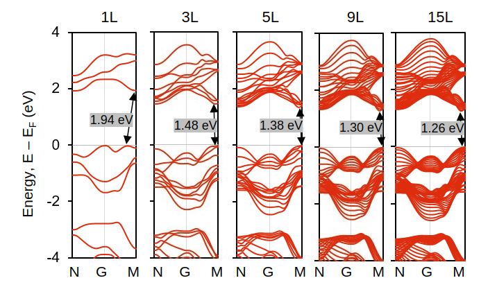
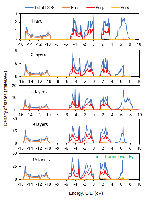
Figures 8 and 9 show the GGA calculated band structure and density of states (DOS) respectively for the free-standing t-Se surface slabs at one, three, five, nine, and fifteen layers. Analysis of these plots shows that the top of the valence band and the bottom of the conduction bands are dominated by the Se orbitals as like the case of the bulk Se. As the number of layers increases, the overall features of band composition and the density of states remain similar except the valence band maximum (VBM) shifting from G to M. However, the conduction band minimum (CBM) remains at the same point (near to M). There is an indirect to direct band gap transition as the number of layer increases.
The calculations of the bulk t-Se electronic properties including the direct and indirect band gaps and the corresponding DOS are shown in Section 5.2 of the Supplemental Material in Figures 15 and 16. Starting from few atomic layers, the DOS at the Fermi level and near CBM are very similar to that of the bulk. GGA + vdW calculated band structures and DOS are similar to the GGA calculated features with a slightly lower band gaps.
3.4 Optical Properties
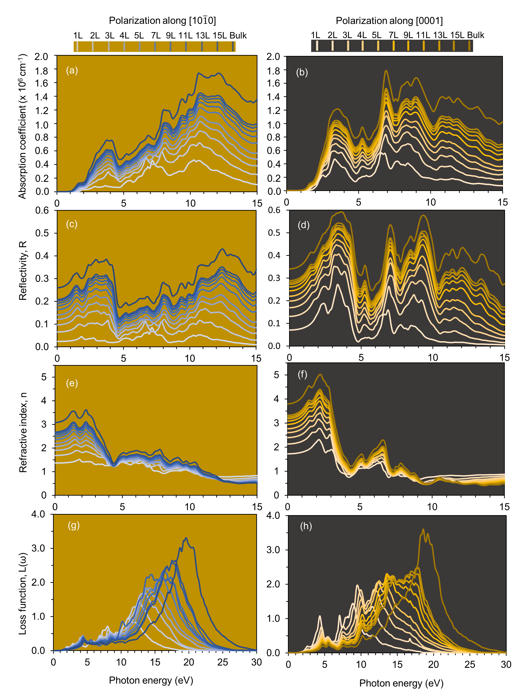
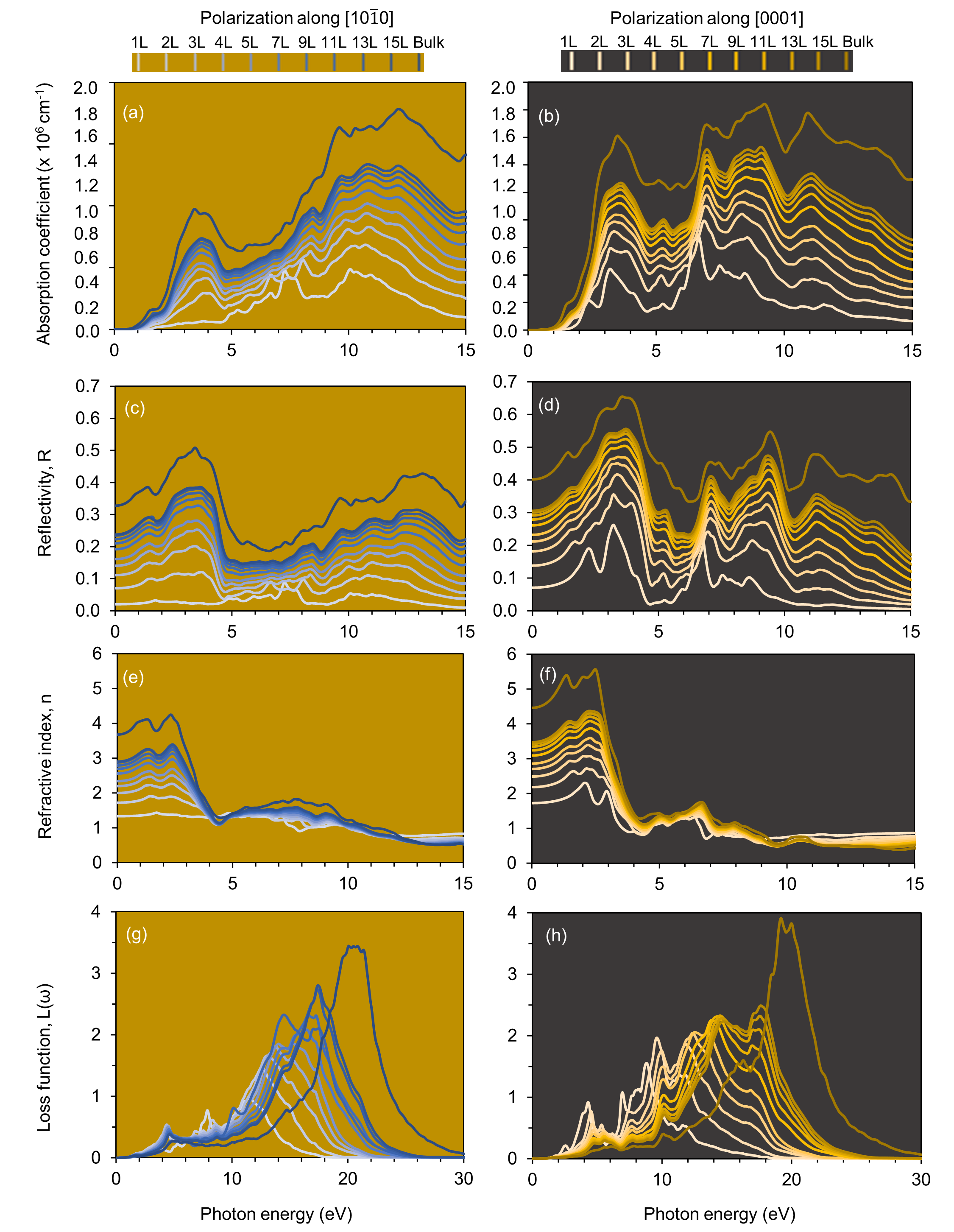
Using the analysis presented above, the optical properties of t-Se are calculated using GGA and GGA+vdW across the photon energy range of interest and along the orientations and [0001], as shown in Figures 10 and 11 for relaxed free standing layers. We focus our analysis on the behavior of the optical absorption coefficient (), the reflectivity (R), the refractive index (n), and the loss function (L).
Some important observations which are apparent when comparing the optical absorption coefficient in the range relevant for the VUV spectrum of noble element detectors (e.g. 7.1 - 9.7 eV): i) after only a few atomic layers the behavior quickly begins to mimic the bulk properties suggesting that extremely thin-films will have a favorable absorption coefficient, ii) the absorption peaks near the area of our interest (9 eV) in both polarizations and thus should have very favorable properties sought in their application as a VUV photodetector.
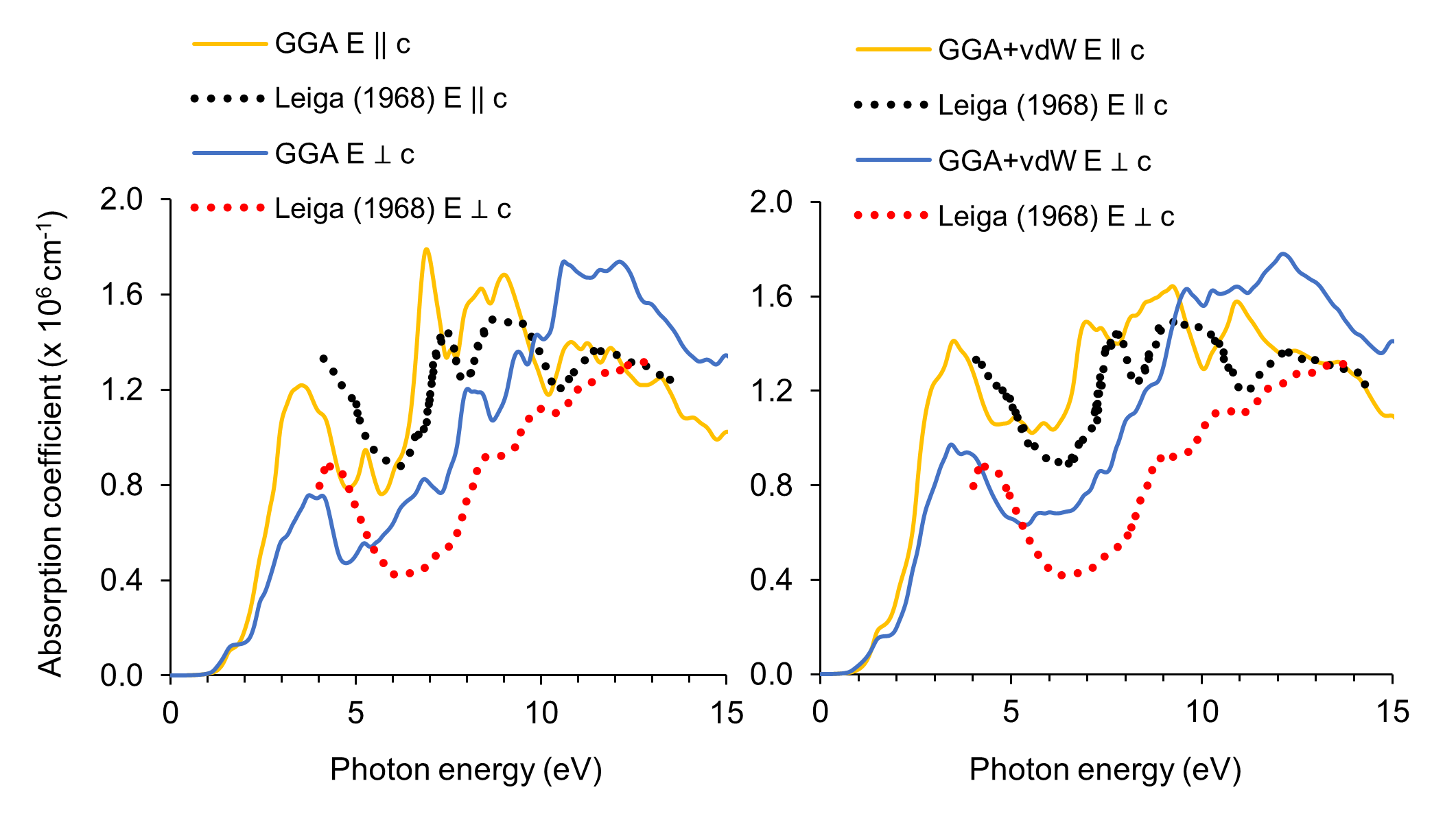
Figure 12 shows the bulk calcuations compared to data from references [24] and [25] taken for -Se when the incident radiation is parallel and perpindicular to the Se crystal over the photon energy range of 4-14 eV. The broad spectral features show general agreement while the two data sets differ from the GGA and GGA+vdW values by 10-20% with the data being generally higher than the calculation for photon energies <5 eV and the calculations being higher than the data above 5 eV.
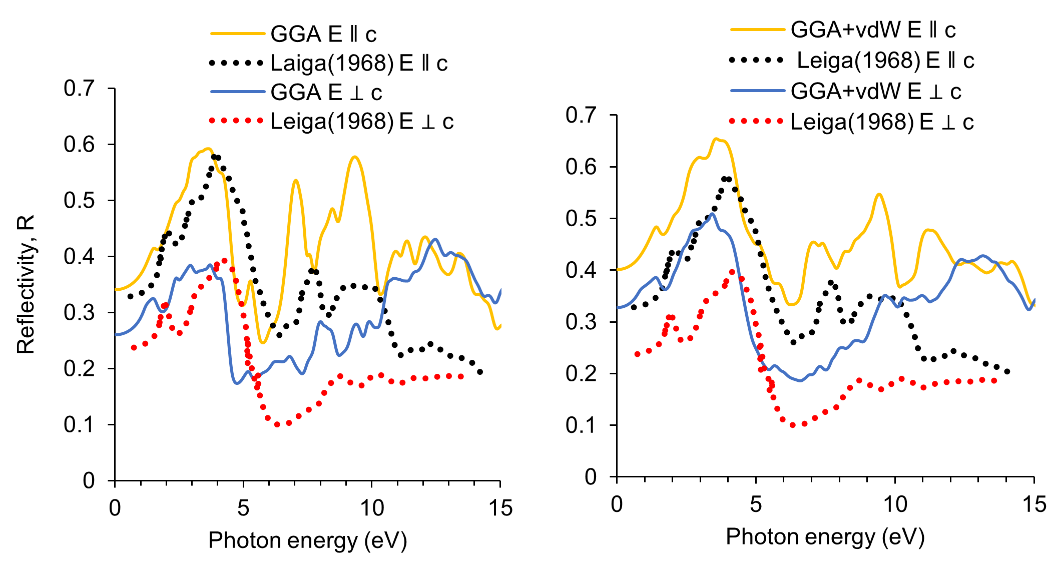
A similar analysis of the reflectance in Figure 10 and 11 shows: i) again, after only a few atomic layers the behavior quickly begins to mimic the bulk properties, ii) the reflectivity is 30% higher for the [0001] orientation compared to the for both GGA and GGA+vdW, iii) the GGA+vdW calculation has a higher predicted reflectance in the region between 1-6 , above which GGA and GGA+vdW agree with one another. Comparing our results to data a few conclusions can be drawn. Firstly, the broad spectral features show a similarity between the GGA calculation, GGA+vdW, and the data with peaks and drops occurring in roughly the same energies. In t-Se the dip shown in the data around 6.5 eV and its rise thereafter is interpreted as a gap in the valence band. A similar, albeit, shifted phenomenon is seen in both the GGA and GGA+vdW calculation with the GGA+vdW more closely matching the data in the region of the dip. Secondly, the magnitude of the reflectance in the region of interest (7 eV - 9 eV) seems to be lower in the GGA calculation than the data by about 40% and slightly less low in the GGA+vdW.
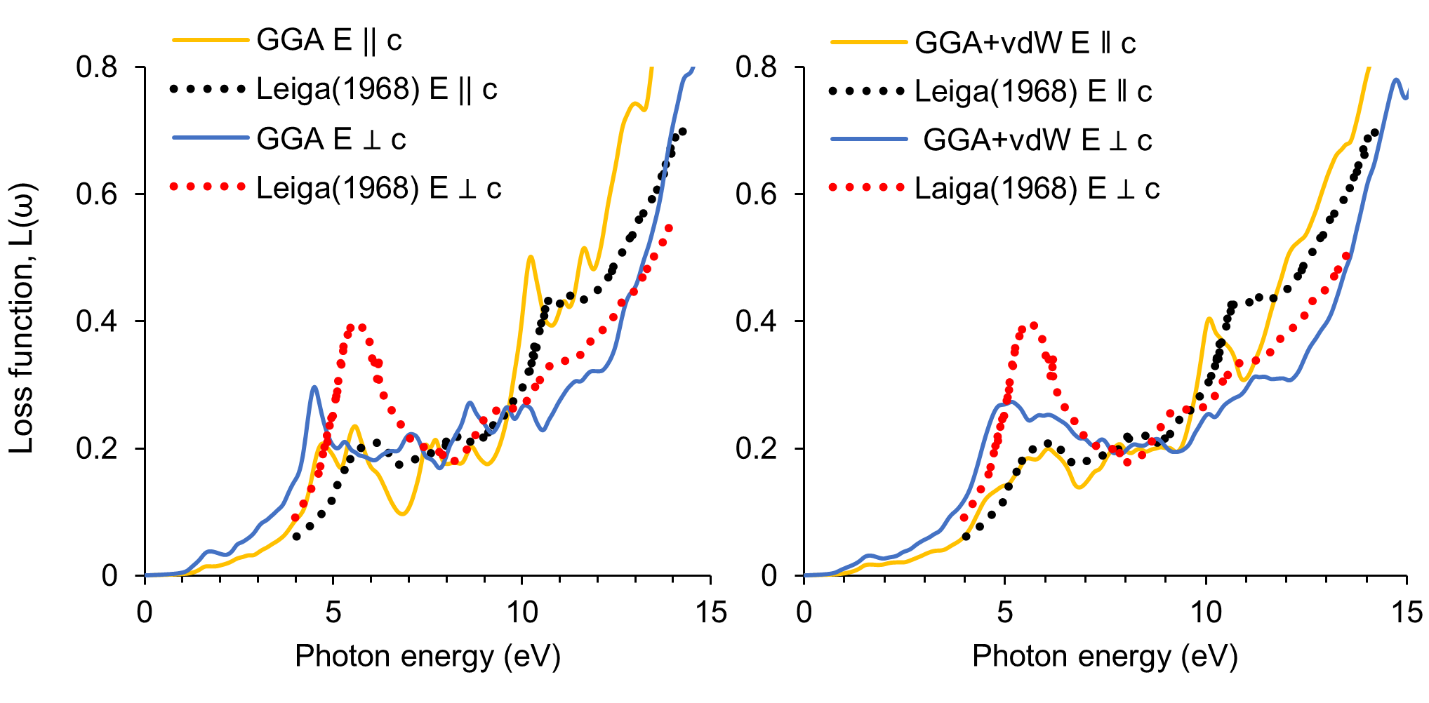
Similar comparisons for the index of refraction and the loss function follow with subsequent comparisons to data in Figure 14 having generally the same conclusions as those given above.
4 Conclusion
In this work, we have employed density functional theory to systematically investigate the thermodynamic, electronic and optical properties of surface layers of trigonal selenium (t-Se). We find that within few atomic layers of t-Se, free standing thin films started to have bulk like properties. From the electronic structures calculations, both the valence and the conduction bands’ extrema (VBM and CBM) have Se- characters, so optical absorption across the band gap is highly suppressed. In addition, an indirect to direct band gap transition was observed as the number of layers increases within the slab. Overall, the optical properties matches well with the experimental results when Van der Waals corrections are included in the DFT Hamiltonian. The optical absorption peaks near the area of our interest (9 eV) and thus should have very favorable properties sought in their application as a VUV photodetector.
This work serves as a foundational starting point for theoretical calculations to better understand the properties a selenium based detector will have for photons in the VUV spectrum. The calculations have shown the surface energy, work function, electronic, and optical properties which can be derived for t-Se. Where possible, the calculations are compared to existing data. The general agreement found between the existing data for t-Se and the work done here opens up the doorway to further analysis of the amorphous state (a-Se), which is most commonly used in photon detectors and helps better understand the fundamental properties of the thin film selenium detectors which can be employed for VUV photon detection given Se’s favorable properties of high absorption coefficient, low loss function, and favorable transport properties.
Acknowledgments
All computations for this work were executed in Texas Advanced Computing Center (TACC) at Austin, TX. This work was supported by a grant from the U.S. Department of Energy, Office of Science, Office of High Energy Physics under Award Number DE-SC 0000253485.
Conflict of Interest and Data Sharing
The authors declare no conflict of interest in this work. The data that support the findings of this study are available from the corresponding author upon reasonable request.
References
- [1] Effect of light on selenium during the passage of an electric current, Nature 7 (Feb, 1873) 303–303.
- [2] W. Smith, The action of light on selenium, Journal of the Society of Telegraph Engineers 2 (Feb, 1873) 31–33.
- [3] F. Fordyce, Selenium Geochemistry and Health, AMBIO: A Journal of the Human Environment 36 (2007), no. 1 94 – 97.
- [4] S. Tutihasi and I. Chen, Optical properties and band structure of trigonal selenium, Phys. Rev. 158 (Jun, 1967) 623–630.
- [5] H. T. Li and P. J. Regensburger, Photoinduced discharge characteristics of amorphous selenium plates, Journal of Applied Physics 34 (1963), no. 6 1730–1735, [https://doi.org/10.1063/1.1702669].
- [6] R. P. Sechak, Tri-layer selenium doped photoreceptor, 1972.
- [7] J. Rowlands and S. Kasap, Amorphous semiconductors usher in digital x-ray imaging, Physics Today 50 no. 11 24.
- [8] S. Kasap and J. Rowlands, Review x-ray photoconductors and stabilized a-se for direct conversion digital flat-panel x-ray image-detectors, Journal of Materials Science: Materials in Electronics 11 (2000), no. 6 179–198, [https://doi.org/10.1023/A:1008993813689].
- [9] T. Masuzawa, I. Saito, T. Yamada, M. Onishi, H. Yamaguchi, Y. Suzuki, K. Oonuki, N. Kato, S. Ogawa, Y. Takakuwa, and et al., Development of an amorphous selenium-based photodetector driven by a diamond cold cathode, Sensors 13 (Oct, 2013) 13744–13778.
- [10] W. Zhao, D. Li, A. Reznik, B. J. M. Lui, D. C. Hunt, J. A. Rowlands, Y. Ohkawa, and K. Tanioka, Indirect flat-panel detector with avalanche gain: Fundamental feasibility investigation for sharp-amfpi (scintillator harp active matrix flat panel imager), Medical Physics 32 (2005), no. 9 2954–2966, [https://aapm.onlinelibrary.wiley.com/doi/pdf/10.1118/1.2008428].
- [11] T. Nakada and A. Kunioka, Polycrystalline thin-film TiO2/se solar cells, Japanese Journal of Applied Physics 24 (jul, 1985) L536–L538.
- [12] H. Ito, M. Oka, T. Ogino, A. Takeda, and Y. Mizushima, Selenium thin film solar cell, Japanese Journal of Applied Physics 21 (jan, 1982) 77.
- [13] T. K. Todorov, S. Singh, and et. al, Ultrathin high band gap solar cells with improved efficiencies from the world’s oldest photovoltaic material, Nature Communications 8 (Sept, 2017).
- [14] T. Masuzawa, M. Onishi, I. Saito, T. Yamada, A. T. T. Koh, D. H. C. Chua, S. Ogawa, Y. Takakuwa, Y. Mori, T. Shimosawa, and K. Okano, Cover picture: High quantum efficiency uv detection using a-se based photodetector (phys. status solidi rrl 7/2013), physica status solidi (RRL) – Rapid Research Letters 7 (2013), no. 7 [https://onlinelibrary.wiley.com/doi/pdf/10.1002/pssr.201370438].
- [15] S. Abbaszadeh, K. S. Karim, and V. Karanassios, Measurement of uv from a microplasma by a microfabricated amorphous selenium detector, IEEE Transactions on Electron Devices 60 (2013), no. 2 880–883.
- [16] M. Zhu, G. Niu, and J. Tang, Elemental se: fundamentals and its optoelectronic applications, J. Mater. Chem. C 7 (2019) 2199–2206.
- [17] K. Majumdar and K. Mavrokoridis, Review of liquid argon detector technologies in the neutrino sector, Applied Sciences 11 (2021), no. 6.
- [18] L. Baudis, Wimp dark matter direct-detection searches in noble gases, Physics of the Dark Universe 4 (2014) 50–59. DARK TAUP2013.
- [19] M. Kuźniak and A. M. Szelc, Wavelength shifters for applications in liquid argon detectors, Instruments 5 (2021), no. 1.
- [20] K. Ieki et al., Large-Area MPPC with Enhanced VUV Sensitivity for Liquid Xenon Scintillation Detector, Nucl. Instrum. Meth. A 925 (2019) 148–155, [arXiv:1809.08701].
- [21] J. Asaadi, B. J. P. Jones, A. Tripathi, I. Parmaksiz, H. Sullivan, and Z. G. R. Williams, Emanation and bulk fluorescence in liquid argon from tetraphenyl butadiene wavelength shifting coatings, JINST 14 (2019), no. 02 P02021, [arXiv:1804.00011].
- [22] Y. Abraham et al., Wavelength-Shifting Performance of Polyethylene Naphthalate Films in a Liquid Argon Environment, arXiv:2103.03232.
- [23] W. Ootani, K. Ieki, T. Iwamoto, D. Kaneko, T. Mori, S. Nakaura, M. Nishimura, S. Ogawa, R. Sawada, N. Shibata, Y. Uchiyama, K. Yoshida, K. Sato, and R. Yamada, Development of deep-uv sensitive mppc for liquid xenon scintillation detector, Nuclear Instruments and Methods in Physics Research Section A: Accelerators, Spectrometers, Detectors and Associated Equipment 787 (2015) 220–223. New Developments in Photodetection NDIP14.
- [24] A. G. Leiga, Optical properties of trigonal selenium in the vacuum ultraviolet, J. Opt. Soc. Am. 58 (Jul, 1968) 880–884.
- [25] A. G. Leiga, Optical properties of amorphous selenium in the vacuum ultraviolet, J. Opt. Soc. Am. 58 (Nov, 1968) 1441–1445.
- [26] P. Hohenberg and W. Kohn, Inhomogeneous electron gas, Phys. Rev. 136 (Nov, 1964) B864–B871.
- [27] W. Kohn and L. J. Sham, Self-Consistent Equations Including Exchange and Correlation Effects, Physical Review 140 (nov, 1965) A1133–A1138, [PhysRev.140.A1133].
- [28] P. E. Blöchl, Projector augmented-wave method, Phys. Rev. B 50 (Dec, 1994) 17953–17979.
- [29] G. Kresse and D. Joubert, From ultrasoft pseudopotentials to the projector augmented-wave method, Phys. Rev. B 59 (Jan, 1999) 1758–1775.
- [30] G. Kresse and J. Furthmüller, Efficiency of ab-initio total energy calculations for metals and semiconductors using a plane-wave basis set, Computational Materials Science 6 (1996), no. 1 15 – 50.
- [31] G. Kresse and J. Furthmüller, Efficient iterative schemes for ab initio total-energy calculations using a plane-wave basis set, Phys. Rev. B 54 (Oct, 1996) 11169–11186.
- [32] K. Momma and F. Izumi, VESTA3 for three-dimensional visualization of crystal, volumetric and morphology data, Journal of Applied Crystallography 44 (Dec, 2011) 1272–1276.
- [33] J. P. Perdew, K. Burke, and M. Ernzerhof, Generalized gradient approximation made simple, Phys. Rev. Lett. 77 (Oct, 1996) 3865–3868.
- [34] J. P. Perdew, K. Burke, and M. Ernzerhof, Generalized gradient approximation made simple [phys. rev. lett. 77, 3865 (1996)], Phys. Rev. Lett. 78 (Feb, 1997) 1396–1396.
- [35] S. Grimme, J. Antony, S. Ehrlich, and H. Krieg, A consistent and accurate ab initio parametrization of density functional dispersion correction (dft-d) for the 94 elements h-pu, The Journal of Chemical Physics 132 (2010), no. 15 154104, [https://doi.org/10.1063/1.3382344].
- [36] S. Grimme, J. Antony, S. Ehrlich, and H. Krieg, A consistent and accurate ab initio parametrization of density functional dispersion correction (dft-d) for the 94 elements h-pu, The Journal of Chemical Physics 132 (2010), no. 15 154104, [https://doi.org/10.1063/1.3382344].
- [37] R. Wyckoff, Crystal structures, selenium, .
- [38] P. Cherin and P. Unger, The crystal structure of trigonal selenium, Inorganic Chemistry 6 (1967), no. 8 1589–1591, [https://doi.org/10.1021/ic50054a037].
- [39] D. Vanderbilt and J. D. Joannopoulos, Total energies in se. i. the trigonal crystal, Phys. Rev. B 27 (May, 1983) 6296–6301.
- [40] B. Farid and R. W. Godby, Cohesive energies of crystals, Phys. Rev. B 43 (Jun, 1991) 14248–14250.
- [41] J. C. Boettger, Nonconvergence of surface energies obtained from thin-film calculations, Phys. Rev. B 49 (Jun, 1994) 16798–16800.
- [42] S. K. Barman and M. N. Huda, Mechanism behind the easy exfoliation of ga2o3 ultra-thin film along (100) surface, physica status solidi (RRL) – Rapid Research Letters 13 (2019), no. 5 1800554, [https://onlinelibrary.wiley.com/doi/pdf/10.1002/pssr.201800554].
- [43] S. A. Moten, R. Atta-Fynn, A. K. Ray, and M. N. Huda, Size effects on the electronic and magnetic properties of puo2 (111) surface, Journal of Nuclear Materials 468 (2016) 37 – 45.
- [44] E. Bainglass and M. N. Huda, Low-index stoichiometric surfaces of cubiw2o8, Surface Science 705 (2021) 121762.
- [45] N. D. Alkhaldi, S. K. Barman, and M. N. Huda, Crystal structures and the electronic properties of silicon-rich silicon carbide materials by first principle calculations, Heliyon 5 (2019), no. 11 e02908.
- [46] L.-H. Lee, Solid surface tensions of amorphous and crystalline selenium, Journal of Non-Crystalline Solids 6 (1971), no. 3 213–220.
- [47] G. Guisbiers, S. Arscott, and R. Snyders, An accurate determination of the surface energy of solid selenium, Applied Physics Letters 101 (2012), no. 23 231606, [https://doi.org/10.1063/1.4769358].
- [48] J. P. Perdew, Density functional theory and the band gap problem, International Journal of Quantum Chemistry 28 (1985), no. S19 497–523, [https://onlinelibrary.wiley.com/doi/pdf/10.1002/qua.560280846].
- [49] J. P. Perdew, W. Yang, K. Burke, Z. Yang, E. K. U. Gross, M. Scheffler, G. E. Scuseria, T. M. Henderson, I. Y. Zhang, A. Ruzsinszky, H. Peng, J. Sun, E. Trushin, and A. Görling, Understanding band gaps of solids in generalized kohn–sham theory, Proceedings of the National Academy of Sciences 114 (2017), no. 11 2801–2806, [https://www.pnas.org/content/114/11/2801.full.pdf].
5 Supplemental Material
First principles studies of the surface and opto-electronic properties of ultra-thin t-Se
S. K. Barman, M. N. Huda, J. Asaadi, E. Gramellini, D. Nygren
5.1 Surface Properties
| Surface area of free-standing laryers (Å2) | ||
|---|---|---|
| Number of layers | GGA | GGA + vdW |
| 1 | 21.08 | 20.29 |
| 2 | 21.91 | 20.84 |
| 3 | 22.23 | 21.08 |
| 4 | 22.36 | 21.17 |
| 5 | 22.44 | 21.22 |
| 6 | 22.52 | 21.32 |
| 7 | 22.62 | 21.35 |
| 8 | 22.64 | 21.41 |
| 9 | 22.61 | 21.43 |
| 10 | 22.64 | 21.46 |
| 11 | 22.77 | 21.46 |
| 12 | 22.71 | 21.46 |
| 13 | 22.68 | 21.44 |
| 14 | 22.73 | 21.51 |
| 15 | 22.74 | 21.53 |
| Surface energies, ) for surface slabs of t-Se | ||
|---|---|---|
| Number of layers in slabs | GGA | GGA |
| 1 | 160.22 | 176.24 |
| 2 | 160.22 | 192.26 |
| 3 | 160.22 | 192.26 |
| 4 | 160.22 | 192.26 |
| 5 | 160.22 | 192.26 |
| 6 | 160.22 | 192.26 |
| 7 | 160.22 | 192.26 |
| 8 | 160.22 | 192.26 |
| 9 | 160.22 | 192.26 |
| 10 | 160.22 | 192.26 |
| 11 | 160.22 | 192.26 |
| 12 | 160.22 | 176.24 |
| 13 | 160.22 | 176.24 |
| 14 | 160.22 | 176.24 |
| 15 | 160.22 | 176.24 |
| Slab Thickness (Å) | ||
|---|---|---|
| Number of layers in slabs | GGA | GGA + vdW |
| 2 | 4.583 | 4.283 |
| 3 | 9.056 | 8.531 |
| 4 | 14.592 | 12.690 |
| 5 | 18.065 | 16.903 |
| 6 | 22.628 | 21.123 |
| 7 | 27.150 | 29.614 |
| 8 | 31.568 | 29.614 |
| 9 | 36.109 | 33.788 |
| 10 | 40.604 | 38.081 |
| 11 | 45.087 | 42.232 |
| 12 | 49.604 | 46.427 |
| 13 | 54.102 | 50.576 |
| 14 | 58.617 | 54.919 |
| 15 | 63.045 | 59.217 |
5.2 Bulk Electronic Properties