From English to PCSEL: LLM helps design and optimize photonic crystal surface emitting lasers
Abstract
Conventional design and optimization of Photonic Crystal Surface Emitting Lasers (PCSEL) usually requires expert knowledge in semiconductor physics and optimization algorithms, which is also known as the inverse design problem. However, with the trend towards automation and depersonalization of the entire integrated circuits (IC) industry, the conventional method, with the drawback of being relatively labor-intensive and sub-optimal, warrants further refinement. This technical dilemma remained until the emergence of Large Language Models (LLMs), such as OpenAI’s ChatGPT and Google’s Bard. This paper explores the possibility of applying LLMs to machine learning-based design and optimization of PCSELs. Specifically, we utilize GPT-3.5 and GPT-4. By simply having conversations, GPT assisted us with writing Finite Difference Time Domain (FDTD) simulation code and deep reinforcement learning code to acquire the optimized PCSEL solution, spanning from the proposition of ideas to the realization of algorithms. Given that GPT will perform better when given detailed and specific questions, we break down the PCSEL design problem into a series of sub-problems and converse with GPT by posing open-ended heuristic questions rather than definitive commands. This paper shows that LLMs, such as ChatGPT, can guide the nanophotonic design and optimization processes, on both the conceptual and technical level, and we propose new human–AI co-design strategies and show their practical implications. We achieve a significant milestone for the first step towards an automated end-to-end nanophotonic design and production pipeline.
1 Introduction
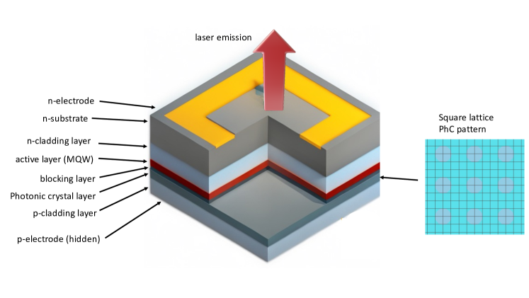
Trends of design automation and depersonalization (i.e., human out of the loop) in the integrated circuit (IC), nanotechnology, and semiconductor industries [1, 2] are emerging rapidly. Aided by artificial intelligence (AI), machine automation is beginning to replace conventional design and fabrication processes involving humans that had existed for over half a century. The nanophotonics industry [3, 4], however, has not yet been sufficiently depersonalized due to its unique fabrication precision requirements [5, 6] and relatively complex theoretical models [7, 8]. As an important example of nanophotonics, the design of photonic-crystal-surface-emitting-lasers (PCSEL) [9, 16, 17, 18, 19, 20, 21, 22, 23, 10, 11, 12, 13, 14, 15, 8], such as the one shown in Figure 1, demand rigorous physical modelling and calculations with Finite Difference Time Domain (FDTD) or Finite Element Analysis (FEA) simulation tools. However, the inverse design and optimization [24, 25] of PCSEL suffers from three aspects: the one-to-many mapping nature and non-convexity of this inverse problem, a high demand for expert knowledge in semiconductor physics and theoretical modelling/simulation (and thus human involvement), and a lack of ready-to-use machine learning algorithms. The above challenges make it difficult to achieve an ene-to-end depersonalized design pipeline for PCSELs.
Luckily, recent advancements in machine learning [26] and optimization algorithms [27] have propelled the progress of depersonalized nanophotonics design. Early in the 90s, heuristic, evolutionary [28], and gradient-based [29] optimization algorithms began to emerge prolifically. Key algorithms include Newton’s method [30], particle swarm [31], genetic algorithm [32], Bayesian optimization [33], Monte Carlo method [34], and simulated annealing [35] etc. These algorithms provide a new way of thinking when facing these non-convex optimization problems, which act as a solid foundation for continued research. But the problem remains for heavy human involvement due to sophisticated trial-and-error iterations. To solve this, at around 2012, researchers proposed deep-learning (DL) [36, 26] frameworks in order to construct a mapping relationship between input parameters and output targets. In particular, DL consists of supervised, unsupervised, and reinforcement learning (RL) [37]. These DL models greatly bolstered the efficiency of nanophotonic inverse design, pushing the possibility of automated and depersonalized design into a new stage [38, 25, 39, 40]. Circa 2023, a new DL framework based on RL (e.g., deep Q-learning (DQN) [41]), called Learning to Design Optical-Resonators (L2DO) [42], provides the solution for autonomous inverse design of photonic crystal nanocavities without human intervention. With two orders of magnitude higher sample efficiency compared to supervised learning, L2DO has preliminarily realized photonics design automation on an algorithmic level. However, since both the simulation code and DL code in L2DO were still created by the human designer, we were still a distance away from depersonalized photonic design.
Development of large language models (LLMs) [43, 44, 45, 46, 47] is the final building block of depersonalized nanophotonics designs. LLMs are recent advances in deep learning to work on human languages and natural language processing. Behind the scene, it is a large-scale pre-trained attention-based transformer model that predicts and generates human-like text output. LLMs are trained on massive amounts of text data collected from the internet, which includes books, articles, websites, google searches, and various other sources. LLMs have been rapidly evolving in the last few years. Word2Vec [48], developed by Google’s Tomas Mikolov in 2013, is a milestone in the development of LLM. It generates high-quality word embeddings (representing words as vectors in a high-dimensional space) to capture semantic meaning and relationships. Following this model were The Global Vectors for Word Representation (GloVe) [49] model, developed by Stanford researchers in 2014, and Seq2Seq [50] models, which was also introduced by Google. These two models perform better at scalability than the former and could be trained in parallelized way, thus more efficient. Along with these two models, the concept of attention mechanism was proposed, introducing weight coefficients to words in different positions. In 2018, BERT [51] were brought to us by Google. However, LLMs did not take center stage of the world until these last few months, with the introduction of GPT-3 [52], followed by GPT-3.5 and eventually GPT-4. GPT-4 is undoubtedly a pioneering breakthrough which is bound to bring a revolutionary change in many scientific and engineering realms.
A limited handful of researchers have found the potential for using LLMs in hardware design and implementation at an early time. In 2020, researchers utilized an improved GPT-2 model called "DAVE" for Verilog code snippets generation and output evaluation [53], which is a crucial component in IC design pipeline. A more recent model named "Chip-chat" [2] came out in 2023, which is an LLM-driven method for IC Verilog code generation and is one of the first wholly-AI-written Hardware Description Language (HDL) for chip tape-out. Meanwhile, LLMs have also contributed significantly to the design and control of robots. Researchers have shown the guidance value of LLM in a robotic gripper design process [54], both conceptually and technically. By means of simply conversing with GPT, they successfully designed a robotic gripper capable of reaping the tomato plant. Last but not least, a method based on LLMs called "SayCan" [55], proposed by a team from Google, has recently enabled leveraging and grounding the rich knowledge in large language models to complete embodied tasks by robot.
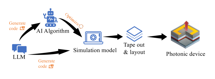
In this work, we propose a new human–AI co-design strategy for PCSELs and show the practical implications of LLMs for nanophotonic design methodology in general. Specifically, we explored and verified the potential of applying LLMs to machine learning-based design and optimization of PCSELs, during which we seek to maintain as less human involvement as possible. In other words, the human is merely a facilitator rather than the person in charge. By simply having conversations spanning from the proposition of initial ideas to the implementation of final algorithms, GPT-4 assisted us with writing FDTD simulation code and deep RL (e.g. DQN) code to acquire the optimized PCSEL solution. The resulting PCSEL is single-mode, high-power, large-area, and small-divergence angle. The whole design pipeline is illustrated in Figure 2. Given that GPT will perform better when given detailed and specific questions, we break down the PCSEL design problem into a series of sub-problem modules and converse with GPT by strictly posing open-ended heuristic questions rather than definitive commands. This paper shows that LLMs, such as ChatGPT, can guide the nanophotonic design and optimization processes, on both the conceptual and technical level. All in all, we achieve a significant milestone for the first step towards an automated end-to-end nanophotonic design and optimization pipeline.
2 Methods
2.1 Objective overview
Photonic Crystal Surface Emitting Lasers (PCSELs) [9, 17, 16] are a type of laser that combines the benefits of photonic crystals (PhC) [7] and Vertical Cavity Surface Emitting Lasers (VCSELs) [57]. PhCs are artificial structures that have a periodic refractive index modulation in one, two, or three dimensions. This periodicity creates a bandgap that inhibits the propagation of light in certain frequency ranges. VCSELs are lasers that emit light perpendicular to the surface of the semiconductor structure, which allows for efficient coupling to optical fibers and other optical components. PCSELs combine these two technologies to create lasers that have several advantages over traditional lasers and therefore has the best of both worlds.
The basic design of a PCSEL consists of a PhC layer, an active layer, and several other cladding layers and substrates along with p-n junctions and electrodes at the ends (Figure 1). The PhC layer typically functions as a resonance cavity. The active layer, usually composed of III-V materials (InP/InGaP, GaAs/InGaAs/AlGaAs, GaN/InGaN etc.) which can create a population inversion of charge carriers when the threshold is reached, is placed in the middle of a PCSEL and serves to produce the light that is emitted from the laser. Population inversion means that there are more electrons in higher energy levels than in lower energy levels, which allows for stimulated emission of photons when an electrical current is applied [58, 9]. So when an electrical pumping current is injected into the active layer material, it emits laser light that is ideally confined and amplified within the resonant cavity. Additionally, the active layer could contain quantum dots or quantum wells that increase the recombination rate of spontaneous emission and thus substantially enhance the lasing effect. So the bottom line is that the PhC layer is used to control the amplitude and direction of the emitted light, but the active layer is what actually generates the light. Therefore, proper design of the PhC layer and the active layer plays a central role in the overall quality of a PCSEL.
| Metric/Figure of merit | Target values |
|---|---|
| Lasing area | >= 3.6e-13 |
| Operating wavelength | = 980 nm |
| Output power/injecting power | >= 30% |
| Divergence angle | <= 1 degree |
In this article, we investigate the potential of an LLM-based depersonalized PCSEL design and optimization pipeline (Figure 2). The target metrics or figure of merit of the PCSEL to be designed and optimized are listed in Table 1. We set the target values according to our own experiments and surveying the literature for what is ideal for high-quality PCSEL lasing. For example, the wavelength of 980 nm is important for applications in telecommunications and satellites, a high output power is important for applications like autonomous driving, machining, and medicine, and a small divergence angle is important for achieving high beam quality and long-distance light propagation.
2.2 Human-AI co-design philosophy
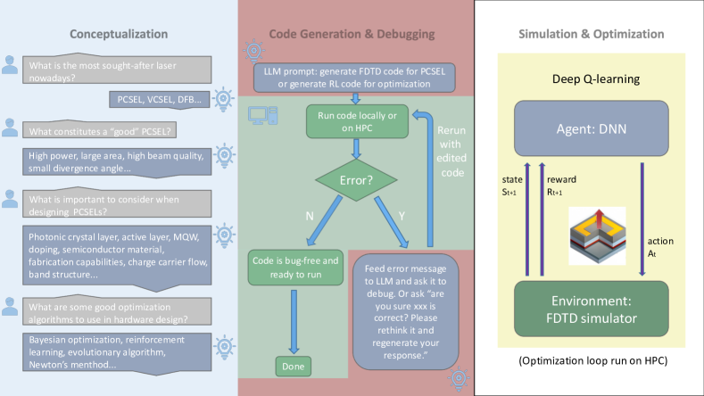
In the near future, LLMs are bound to fundamentally change the design flow in many fields, for its ability to internalize an extensive dataset in different types and generate proper responses using the acquired knowledge. Such potential has been discovered by researchers in the fields of medicine, robotics, literature, topology etc. In this article, we propose a new paradigm for applying LLMs in PCSEL design and optimization, called the "human-AI co-design" methodology (Figure 2 & 3). As illustrated in Figure 3, we divide the design process into three steps: conceptualization, code generating and debugging, and simulation and optimization. Due to the limitation of the status quo of LLMs, the AI agent usually cannot give out the perfect solution all at once. Therefore, the human needs to act as a liaison to help administer/facilitate the design work while simultaneously bearing in mind that excessive human involvement could compromise the integrity of the AI agent’s decisions. So for example if a large proportion of the design task is dominated/controlled by humans, it does not reflect the human-AI co-design philosophy and thus should be avoided as much as possible. Overall, the design flow should follow these rules and restrictions:
1. The whole design process should start with the human providing an open-ended question to GPT rather than giving definitive commands. This is the beginning of an important conceptualization process, where the human stimulates the LLM to brainstorm and generate creative ideas. For example, you can start a conversation by "What is the most sought-after laser nowadays?" or "What are some good optimization algorithms to use in hardware design?" Subsequent conversations will continue by gradually guiding GPT to arrive at a specific solution for this conceptual question. Sample Q&A rounds are demonstrated in the left column of Figure 3. Once we get to the code generations and debugging stage, questions can become more specific and technical, such as "can you help me design a high-power and large-area PCSEL model using FDTD algorithm written in Python?" or "can you help me improve an existing deep-Q learning code implemented with experience replay that’s written with PyTorch?"
2. A well-described problem should be considered to have only a unique optimized solution. During the conversation, GPT might provide several feasible solutions. The existence of a feasible solution space should be an indicator that our prompt question to GPT has not been phrased well. So the correct action is to narrow down the solution space by adding constraints or target metrics to the question so that we could get a unique solution. One can refine their prompt by adding "considering XXX (your numerical targets or constraints), can you give me an optimized solution among which you gave previously?".
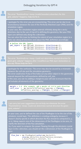
3. Humans should respect the self-correcting mechanism of GPT rather than directly pointing out the problems/errors it has. In the conversations, there might be times when the answers given by LLMs are self-contradictory or simply wrong. This is attributable to GPT’s insufficient understanding of the problem it’s solving, which usually happens at the early stage of a conversation. To properly respect the self-correcting mechanism of GPT, one should report the error by saying "you have just mentioned XXX, and I hope you could think twice about this and regenerate your answer" or "are you sure XXX is the correct answer? Please elaborate" rather than "lines XXX and XXX of the code you generated are wrong" or "fix the XXX function/method in the code for me". In the code generating part, these kinds of mistakes will be especially common. In our experience, it usually takes several conversational iterations before the code finally becomes bug-free and ready to run. When debugging the code, it is not advised that one points out the precise location of error for GPT; the proper way is to copy the error message from the terminal and let AI do the modification itself. A demonstration of this interactive debugging process is shown in the middle column of Figure 3.
2.2.1 Conceptualization with the LLM
The conceptualization step is for AI to have a general understanding of what our problem is about, as a result of which the AI can choose proper methods and algorithms for more detailed prompts down the road. We kick off the conversation by raising a heuristic question "what constitutes a "good" PCSEL laser?" and "let us design a PCSEL together, how do you think we should start?", and the LLM provides us with a general design pipeline by saying "here is a general procedure to get started with" where the design problem is broken down into sub-modules such as "understanding the basics of PCSEL", "material selection", "designing photonic crystal structure" etc. Then we take a further step by asking: "I have understood the basics of PCSEL, now what are some important factors to consider when designing PCSELs?" The LLM then tells us what to look out for when designing PCSELs. Some sample chats are shown in the left column of Figure 3. We then prompted another heuristic question about choosing optimization algorithms. GPT-4 eventually made up its mind by the phrase "In this case, reinforcement learning and Bayesian optimization might be the most suitable for your problem" after we’ve clarified our optimization objectives and constraints. When we think GPT-4 has for the most part understood what we are trying to do, we ask it: "Could you generate an appropriate code skeleton according to the above conversation? Please note that the FDTD should be implemented with meep and RL should be with PyTorch." As a result, GPT-4 gives us a script skeleton template for FDTD simulation using meep [56] and DQN using PyTorch, respectively. The problem has now evolved to how to expand each of these two code templates to a full-blown code, meaning that our work is moving to the next stage for code generation.
2.2.2 Code generation and improvement
Based on section 2.2.1, we have divided the coding problem into two modules (FDTD and DQN) and obtained the initial code skeletons of both modules. In this section we will complete, expand and debug our existing code skeletons, which is the core stage of our whole PCSEL design process.
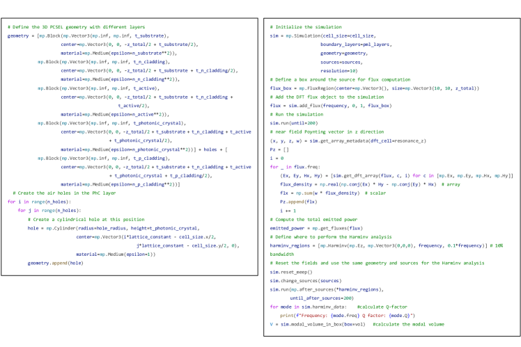
For generating a FDTD simulation code from a skeleton script, we need to provide the LLM with more specific and concrete physical parameters of the PCSEL. We require that our PCSEL has five layers, called "n-substrate layer", "n-cladding layer", "active layer", "photonic crystal layer", "p-cladding layer" respectively, as well as air holes in the PhC layer. It is worth mentioning that the value of parameters, such as the refractive index and the thickness of each layer, could be randomly initialized due to the DQN optimization process we have later on. In the conversations, we assigned those values in-line with a PCSEL model (seen in Figure 1) we built in the past. In addition, we also provided requirements for boundary conditions, meshing resolution, and refractive indices etc. After we provided the concrete physical parameters, GPT-4 expanded our code by completing the PCSEL structure and simulation settings, as shown in Figure 4. Additionally, the flux and farfield monitors are added according to our requirement for calculating the emitting power, modal volume, and divergence angle; the Harminv monitor is added for calculating the Q-factor. Those monitors and their calculations are shown in Figure 4.
Now that the FDTD simulation code has been written, the next step is doing some debugging and fine-tuning until the code finally runs successfully. As the middle column of Figure 3 and Figure 5 shows, we iteratively test run the code on our local computer and transfer the error messages to GPT for debugging, repeating this process until the code becomes bug-free. In our experience, so long as the errors are not too severe, most bugs can be eliminated within 5 iterations.
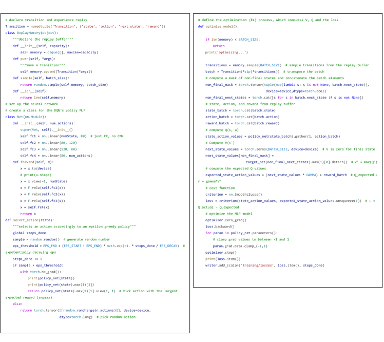
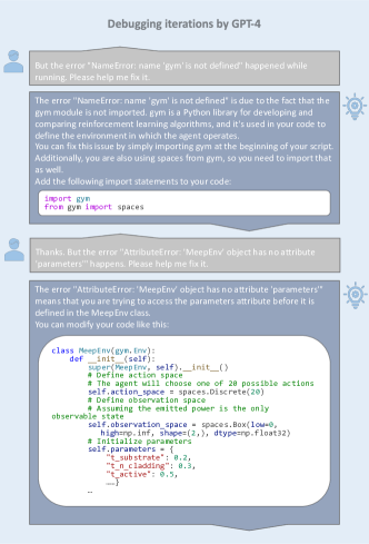
Next, we generated the DQN code for RL-based optimization of PCSELs. As a core component of the DQN algorithm, we first need an environment to provide the feedback interface. We adopted openAI gym [59] as the wrapper class for our environment, which is the FDTD simulator that we have generated and fine-tuned. When letting GPT generate the code for the environment, we told GPT what the state space, action space, and reward function are. Further specifications such as the step size of actions, the upper and lower bounds of state variables are given to GPT as well. Then, with the environment code, we could complete and implement our DQN code. A main DQN script is finished by GPT based on the code skeleton given earlier, considering requirements for the replay buffer, policy DNN, optimizer, loss function etc. See Figure 6 for a part of the completed DQN script. Please note that the DQN script imports the environment class. The next step is to run the DQN code, letting it interact with our FDTD environment and continuously optimize the PCSEL device.
Just like the FDTD code, the DQN code is then debugged and fine-tuned by iteratively running the code and feeding error messages to GPT. An example of this process is demonstrated in Figure 7.
2.2.3 Final optimization step with RL
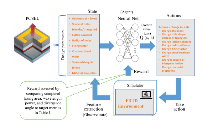
For the full optimization loop of PCSEL using DQN, refer to Figure 8. The main framework is built upon the one proposed in an earlier work [42]. The objective here is to optimize the existing PCSEL structure such that the metrics in Table 1 are met. Therefore at each iteration, computed optical attributes (lasing area, power …) that are closer to the target metrics will earn a higher reward. The state is defined as the design parameters of PCSEL, whereas the action is the changes made to the state at each iteration. The environment, which is a core component of DQN, is realized with the FDTD simulation code we generated earlier. A detailed explanation of the working theories of DQN, the state and action setup, the agent/policy net, and the reward definition are reserved in the supplementary material. The optimization loop is run on an HPC cluster that has 20 CPU cores and 2 GPUs with CUDA, where each trial takes up to 5 days to run.
3 Results and discussion
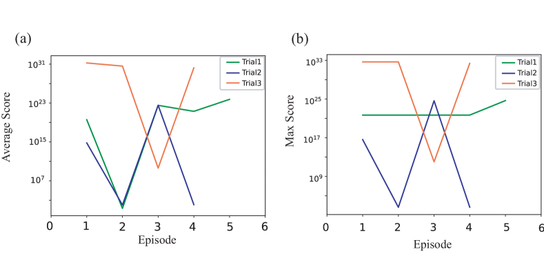
Figure 9 showcases the learning curves (scores vs. episodes) of training the DQN algorithm to optimize our PCSEL according to Figure 8. Three representative trials have been selected to demonstrate the training convergence results. Figure 9(a) shows the average score of each episode, whereas (b) shows the max score of each episode. Each episode contains a maximum of 250 time steps. Each curve, which represents a complete trial, was trained for 5 days until cut off at the end of the 5th day due to limits on computing resources. Details of the score definition are included in the supplementary materials.
Using the optimization results illustrated in Figure 9, the optical attributes of the optimized PCSEL that satisfies the target metrics/figure of merit are reported in Table 2. The corresponding set of design parameters of the optimized PCSEL is included in the supplementary material. To better illustrate the advantage of our results, best data from the literature are listed in the rightmost column of Table 2 for a direct comparison of metrics. The literature data were chosen after an exhaustive literature survey of PCSELs conducted by the authors.
| Metrics | Optimized values | Literature data [17] |
|---|---|---|
| Lasing area | 8.4388e-14 | 6.4e-7 |
| Operating wavelength | 1004.6 nm | 950 nm |
| Output power/injecting power | 81.36% | 6.5 W (c.w.) |
| Divergence angle | 0.5758 degrees | 0.21 degrees |
As the device size and thus the lasing area of the literature data are much larger than ours, we expect the absolute output power of the literature data to be proportionally higher. Nonetheless, since we were able to achieve a high output power-to-injecting power ratio of 80%, our device has a high energy efficiency and electron-to-photon conversion efficiency. This could also mean our device has a high power-density (watts/unit area). Still, the smaller divergence angle reported by the literature data suggests that we still have some work to do for the optimization task, as we were only able to get the divergence down to a lowest of 0.6 degrees. All in all, except for the lasing area which just falls short of the target metric, the rest of the optimized attributes have satisfied and even exceeded the target metrics in Table 1.
Next, when we verified the solved designs in FDTD, we also calculated the resulting Electric field profiles and spectra, which are visualized in the supplementary’s Figure 5. The corresponding FDTD-verified , , and values are also labelled on the plots. According to the profiles in Figure 5(c)-(d), we see that a fundamental or second order resonance mode is achieved by both nanobeam structures, which means that the solved design parameters indeed gave rise to correct electromagnetic mode profiles. According to the spectra in Figure 5(a)-(b), a single resonance peak can be located at the target wavelengths (around 980 nm, respectively), indicating the existence of a single mode and the correctness of the EM modes solved by our algorithm. y-axes of the spectra typically represent the intensity of the EM field measured or simulated while x-axes correspond to wavelengths. These results guarantee a high-quality and precise laser for applications in interconnects on PICs and telecommunications. In future endeavors, experimentalists in our group will fabricate the retrieved designs demonstrated here into actual laser devices, such as the one shown in Figure 1(a)-(b), capable of performing real-world tasks.
4 Conclusion
In summary, this work features the first LLM model applied to inverse designing PCSELs. The inverse problem concerns retrieving a design topology that satisfies certain optical specifications of the photonic device. The model successfully addressed three major challenges faced by state-of-the-art deep learning-enabled inverse design methods: 1) a serious shortage of available training data; 2) the fundamental one-to-many mapping or the non-uniqueness issue; 3) the need for a pre-trained MLP network. According to our studies, the model not only met the required maxima of certain optical responses (e.g., the Q factor) but also optimized some good-to-have features (e.g., modal volume and wavelength) that are conducive to a high-quality laser. The solved values were then verified manually in FDTD and their correctness were confirmed by checking the generated optical responses. We then offered some advice on what hyperparameters need special attention when one attempts to tune a deep RL model. All in all, Our inverse designed laser cavities can find broad applications in modern PICs, interconnects, and telecommunications.
Our methodology in this work is inspired by the famous marriage of AI and Electronic Design Automation (EDA) [1] over the last 5-8 years. For future prospects, this work paves the way for applying deep RL to the rapid multi-objective inverse design and optimization of nanophotonic devices without the need for pre-collecting any data or resorting to human-centered trial-and-error iterations. Through our efforts, we mainly aim to empower the rise of fully automated photonic design because the current state of Photonic Design Automation (PDA) is still largely lacking. Our time and efforts in the subsequent stage will be chiefly directed towards developing a software that brings AI and PDA together into one unity.
Acknowledgement
This work is supported by National Natural Science Foundation of China under Grant No.62174144; Shenzhen Fundamental Research Fund under Grant No.JCYJ20210324115605016 and No.JCYJ20210324120204011; Shenzhen Key Laboratory Project under Grant No.ZDSYS201603311644527; Longgang Key Laboratory Project under Grant No.ZSYS2017003 and No.LGKCZSYS2018000015; Longgang Matching Support Fund No.CXPTPT-2017-YJ-002 and No.201617486; Shenzhen Research Institute of Big Data; President’s Fund (PF01000154); and the Optical Communication Core Chip Research Platform. The authors would like to thank the engineers at the Core Research Facilities (CRF) of SUSTech for their technical support. The authors’d like to thank staff members at ITSO of CUHKSZ for their persistent support for our high-performance computing needs. The authors’d like to thank Mr. Hong Tang for his assistance with GPU CUDA and workstations. The authors’d like to thanks Mr. Ceyao Zhang and Feng Yin for their fruitful discussion on RL and LLMs. The authors’d like to thank Mrs. Xiangying Li for her mental and moral support.
The authors declare no conflict of interests.
Data and Code availability
The data and code are available at: https://github.com/Arcadianlee/. Requests for Meep simulation files should be addressed to Z.Z.
Supplementary material
The associated code, datasets, and supplementary information are available at: https://github.com/Arcadianlee/. Correspondence and requests for materials should be addressed to Z.Z.
Author contributions
Z.Z and R.L. conceived and designed the research project. R.L. and C.Z. designed the models and wrote the code. R.L. performed data post-processing and analysis. W.X. created nanobeam’s simulation files. F.D. prepared supplementary material. H.D. and Z.C. made CAD drawings and schematics. F.Y. and Z.Z. supervised and mentored the project. R.L and C.Z. wrote the paper. Z.Z. managed and funded the research.
References
- [1] Azalia Mirhoseini et al. “A graph placement methodology for fast chip design” In Nature 594.7862 Nature Publishing Group, 2021, pp. 207–212
- [2] Jason Blocklove, Siddharth Garg, Ramesh Karri and Hammond Pearce “Chip-Chat: Challenges and Opportunities in Conversational Hardware Design” In arXiv preprint arXiv:2305.13243, 2023
- [3] Vilson R Almeida, Carlos A Barrios, Roberto R Panepucci and Michal Lipson “All-optical control of light on a silicon chip” In Nature 431.7012 Nature Publishing Group UK London, 2004, pp. 1081–1084
- [4] David Thomson et al. “Roadmap on silicon photonics” In Journal of Optics 18.7 IOP Publishing, 2016, pp. 073003
- [5] Andy Eu-Jin Lim et al. “Review of silicon photonics foundry efforts” In IEEE Journal of Selected Topics in Quantum Electronics 20.4 IEEE, 2013, pp. 405–416
- [6] CH Chiu et al. “Nanoscale epitaxial lateral overgrowth of GaN-based light-emitting diodes on a SiO2 nanorod-array patterned sapphire template” In Applied Physics Letters 93.8 AIP Publishing, 2008
- [7] Qimin Quan, Parag B Deotare and Marko Loncar “Photonic crystal nanobeam cavity strongly coupled to the feeding waveguide” In Applied Physics Letters 96.20 American Institute of Physics, 2010, pp. 203102
- [8] T Inoue et al. “Design of photonic-crystal surface-emitting lasers with enhanced in-plane optical feedback for high-speed operation” In Optics Express 28.4 Optica Publishing Group, 2020, pp. 5050–5057
- [9] Kazuyoshi Hirose et al. “Watt-class high-power, high-beam-quality photonic-crystal lasers” In Nature photonics 8.5 Nature Publishing Group, 2014, pp. 406–411
- [10] D Ohnishi, K Sakai, M Imada and S Noda “Continuous wave operation of surface emitting two-dimensional photonic crystal laser” In Electronics Letters 39.7 The Institution of Engineering & Technology, 2003, pp. 1
- [11] Kou Gondaira et al. “Control of radiation angle by introducing symmetric end structure to oblique waveguide in three-dimensional photonic crystal” In Optics Express 24.12 Optica Publishing Group, 2016, pp. 13518–13526
- [12] Yoshitaka Kurosaka, Kyosuke Sakai, Eiji Miyai and Susumu Noda “Controlling vertical optical confinement in two-dimensional surface-emitting photonic-crystal lasers by shape of air holes” In Optics express 16.22 Optica Publishing Group, 2008, pp. 18485–18494
- [13] William Streifer, D Scifres and Robert Burnham “Coupled wave analysis of DFB and DBR lasers” In IEEE Journal of Quantum Electronics 13.4 IEEE, 1977, pp. 134–141
- [14] Chao Peng et al. “Coupled-wave analysis for photonic-crystal surface-emitting lasers on air holes with arbitrary sidewalls” In Optics Express 19.24 Optica Publishing Group, 2011, pp. 24672–24686
- [15] Masaya Nishimoto, Kyohei Maekawa and Susumu Noda “Design of photonic-crystal surface-emitting lasers with circularly-polarized beam” In Optics Express 25.6 Optica Publishing Group, 2017, pp. 6104–6111
- [16] Susumu Noda et al. “Photonic-crystal surface-emitting lasers: Review and introduction of modulated-photonic crystals” In IEEE Journal of Selected Topics in Quantum Electronics 23.6 IEEE, 2017, pp. 1–7
- [17] Masahiro Yoshida et al. “Double-lattice photonic-crystal resonators enabling high-brightness semiconductor lasers with symmetric narrow-divergence beams” In Nature materials 18.2 Nature Publishing Group UK London, 2019, pp. 121–128
- [18] Seita Iwahashi, Kyosuke Sakai, Yoshitaka Kurosaka and Susumu Noda “Air-hole design in a vertical direction for high-power two-dimensional photonic-crystal surface-emitting lasers” In JOSA B 27.6 Optica Publishing Group, 2010, pp. 1204–1207
- [19] Masaya Nishimoto et al. “Air-hole retained growth by molecular beam epitaxy for fabricating GaAs-based photonic-crystal lasers” In Applied physics express 6.4 IOP Publishing, 2013, pp. 042002
- [20] Seita Iwahashi, Kyosuke Sakai, Yoshitaka Kurosaka and Susumu Noda “Centered-rectangular lattice photonic-crystal surface-emitting lasers” In Physical Review B 85.3 APS, 2012, pp. 035304
- [21] Masahiro Imada et al. “Coherent two-dimensional lasing action in surface-emitting laser with triangular-lattice photonic crystal structure” In Applied physics letters 75.3 American Institute of Physics, 1999, pp. 316–318
- [22] Takuya Inoue et al. “Comprehensive analysis of photonic-crystal surface-emitting lasers via time-dependent three-dimensional coupled-wave theory” In Physical Review B 99.3 APS, 2019, pp. 035308
- [23] Yuhki Itoh et al. “Continous-wave lasing operation of 1.3-m wavelength InP-based photonic crystal surface-emitting lasers using MOVPE regrowth” In Optics Express 28.24 Optica Publishing Group, 2020, pp. 35483–35489
- [24] Wei Ma et al. “Deep learning for the design of photonic structures” In Nature Photonics 15.2 Nature Publishing Group, 2021, pp. 77–90
- [25] Sunae So et al. “Deep learning enabled inverse design in nanophotonics” In Nanophotonics 9.5 De Gruyter, 2020, pp. 1041–1057
- [26] Ian Goodfellow, Yoshua Bengio and Aaron Courville “Deep learning” MIT press, 2016
- [27] Peter R Wiecha et al. “Evolutionary multi-objective optimization of colour pixels based on dielectric nanoantennas” In Nature nanotechnology 12.2 Nature Publishing Group, 2017, pp. 163–169
- [28] Ravi S Hegde “Photonics inverse design: pairing deep neural networks with evolutionary algorithms” In IEEE Journal of Selected Topics in Quantum Electronics 26.1 IEEE, 2019, pp. 1–8
- [29] Jiawei Zhang, Peijun Xiao, Ruoyu Sun and Zhiquan Luo “A single-loop smoothed gradient descent-ascent algorithm for nonconvex-concave min-max problems” In Advances in neural information processing systems 33, 2020, pp. 7377–7389
- [30] Andre Milzarek and Michael Ulbrich “A semismooth Newton method with multidimensional filter globalization for L1-optimization” In SIAM Journal on Optimization 24.1 SIAM, 2014, pp. 298–333
- [31] Zihao Ma and Yu Li “Parameter extraction and inverse design of semiconductor lasers based on the deep learning and particle swarm optimization method” In Optics Express 28.15 Optical Society of America, 2020, pp. 21971–21981
- [32] Yangming Ren et al. “Genetic-algorithm-based deep neural networks for highly efficient photonic device design” In Photonics Research 9.6 Optical Society of America, 2021, pp. B247–B252
- [33] Bobak Shahriari et al. “Taking the human out of the loop: A review of Bayesian optimization” In Proceedings of the IEEE 104.1 IEEE, 2015, pp. 148–175
- [34] Reuven Y Rubinstein and Dirk P Kroese “Simulation and the Monte Carlo method” John Wiley & Sons, 2016
- [35] Dimitris Bertsimas and John Tsitsiklis “Simulated annealing” In Statistical science 8.1 Institute of Mathematical Statistics, 1993, pp. 10–15
- [36] Alex Krizhevsky, Ilya Sutskever and Geoffrey E Hinton “Imagenet classification with deep convolutional neural networks” In Advances in neural information processing systems 25, 2012
- [37] Richard S Sutton and Andrew G Barto “Reinforcement learning: An introduction” MIT press, 2018
- [38] Jiaqi Jiang, Mingkun Chen and Jonathan A Fan “Deep neural networks for the evaluation and design of photonic devices” In Nature Reviews Materials 6.8 Nature Publishing Group, 2021, pp. 679–700
- [39] Renjie Li et al. “Smart and Rapid Design of Nanophotonic Structures by an Adaptive and Regularized Deep Neural Network” In Nanomaterials 12.8 Multidisciplinary Digital Publishing Institute, 2022, pp. 1372
- [40] Renjie Li et al. “Deep learning-based modeling of photonic crystal nanocavities” In Optical Materials Express 11.7 Optical Society of America, 2021, pp. 2122–2133
- [41] Volodymyr Mnih et al. “Human-level control through deep reinforcement learning” In nature 518.7540 Nature Publishing Group, 2015, pp. 529–533
- [42] Renjie Li et al. “Deep reinforcement learning empowers automated inverse design and optimization of photonic crystals for nanoscale laser cavities” In Nanophotonics 12.2 De Gruyter, 2023, pp. 319–334
- [43] Jason Wei et al. “Emergent abilities of large language models” In arXiv preprint arXiv:2206.07682, 2022
- [44] Long Ouyang et al. “Training language models to follow instructions with human feedback” In Advances in Neural Information Processing Systems 35, 2022, pp. 27730–27744
- [45] Mohammad Shoeybi et al. “Megatron-lm: Training multi-billion parameter language models using model parallelism” In arXiv preprint arXiv:1909.08053, 2019
- [46] Takeshi Kojima et al. “Large language models are zero-shot reasoners” In Advances in neural information processing systems 35, 2022, pp. 22199–22213
- [47] Mark Chen et al. “Evaluating large language models trained on code” In arXiv preprint arXiv:2107.03374, 2021
- [48] Tomas Mikolov, Kai Chen, Greg Corrado and Jeffrey Dean “Efficient estimation of word representations in vector space” In arXiv preprint arXiv:1301.3781, 2013
- [49] Jeffrey Pennington, Richard Socher and Christopher D Manning “Glove: Global vectors for word representation” In Proceedings of the 2014 conference on empirical methods in natural language processing (EMNLP), 2014, pp. 1532–1543
- [50] Ilya Sutskever, Oriol Vinyals and Quoc V Le “Sequence to sequence learning with neural networks” In Advances in neural information processing systems 27, 2014
- [51] Jacob Devlin, Ming-Wei Chang, Kenton Lee and Kristina Toutanova “Bert: Pre-training of deep bidirectional transformers for language understanding” In arXiv preprint arXiv:1810.04805, 2018
- [52] Tom Brown et al. “Language models are few-shot learners” In Advances in neural information processing systems 33, 2020, pp. 1877–1901
- [53] Hammond Pearce, Benjamin Tan and Ramesh Karri “Dave: Deriving automatically verilog from english” In Proceedings of the 2020 ACM/IEEE Workshop on Machine Learning for CAD, 2020, pp. 27–32
- [54] Francesco Stella, Cosimo Della Santina and Josie Hughes “How can LLMs transform the robotic design process?” In Nature Machine Intelligence Nature Publishing Group UK London, 2023, pp. 1–4
- [55] Michael Ahn et al. “Do as i can, not as i say: Grounding language in robotic affordances” In arXiv preprint arXiv:2204.01691, 2022
- [56] Ardavan F Oskooi et al. “MEEP: A flexible free-software package for electromagnetic simulations by the FDTD method” In Computer Physics Communications 181.3 Elsevier, 2010, pp. 687–702
- [57] Connie J Chang-Hasnain “Tunable vcsel” In IEEE Journal of Selected Topics in Quantum Electronics 6.6 IEEE, 2000, pp. 978–987
- [58] Simon M Sze, Yiming Li and Kwok K Ng “Physics of semiconductor devices” John wiley & sons, 2021
- [59] Greg Brockman et al. “Openai gym” In arXiv preprint arXiv:1606.01540, 2016