Inverse design of an all-dielectric digitized terahertz optical power splitter by particle swarm optimization method
Abstract
This letter proposes a 50:50 TE terahertz (THz) power splitter based on digitized metamaterials. The device is optimized using particle swarm optimization algorithm. The structure of the digitized metamaterials contains circular air holes in silicon slab which are deposited on silicon dioxide substrate. The optimized structure shows insertion loss (IL) of less than 3.9 dB over the frequency range of 0.9–1.1 THz. The proposed device has the footprint of 400 350 µm2. The proposed device has excellent merits such as compactness, efficient, all-dielectric, and compatible with CMOS fabrication technologies. This device can be used as a vital component in most of the THz circuits to route THz waves.
THz technology has aroused extensive attention of many researchers due to the wonderful properties of THz waves. These waves are applicable in medicine [1, 2, 3], security [4, 5], communication [6, 7, 8], spectroscopy [9, 10, 11] and other numerous applications. Because of the mentioned applications of THz waves, many THz components have been designed for manipulating THz waves, including absorbers [12, 13, 14], power splitters [15, 16, 17, 18, 19], modulators [20, 21, 22], and polarization power spitters [23, 24, 25]. Among these THz components, THz power splitters (TPSs) are of critical importance to route THz waves. Homes et al. proposed a TPS based on silicon slab with several millimeters thickness for utilizing in spectroscopic measurements in a broad THz range (0.2–10 THz) [17]. In 2012, Ung et al. designed and fabricated a TPS by a thin silver sheet deposited on an ultra-thin low-density polyethylene plastic sheet. By changing the thickness of the silver sheet and utilizing its skin depth, they could achieve different splitting ratios. The splitting ratios achieved by transmission and reflection of the metalic-dielectric structure is in the frequency range of 0.5–1.5 THz [16]. In 2013, Hou et al. proposed a TPS based on ferrite photonic crystals. They created line defects in photonic crystals to steer light and also embedded two silicon and ferrite rods at output branches to control various splitting ratios. By applying magnetic field to the ferrite rod, the refractive index of the ferrite rod changes and results in different splitting ratios [19]. In 2016, Reichel et al. designed and fabricated a TPS using T-junction metallic structures. They created metallic waveguides to route THz waves and a mechanical septum to achieve different splitting ratios over a frequency range of 0.15–0.3 THz [18]. In 2017, Yang et al. utilized temperature-dependence photonic crystals for realizing a 1 6 TPS at 1 THz. They used a multi-mode interferometer and four Y splitters that were created using line and point defects in photonic crystals [15]. The mentioned TPSs suffer from need to external magnetic fields that enforce higher fabrication cost [19], larger dimensions [15, 16, 17, 18, 19], inability for integration [16, 17, 18], and working at a narrowband THz spectrum [15].
In this paper we present an all-dielectric compact TPS with ultra-small footprint and compatible with CMOS fabrication technology based on metamateials using inverse design. The inverse design uses particle swarm optimization (PSO) method to optimize the structure for realizing a 50:50 splitting ratio. In this device, we have used digitized structure of air holes in silicon slab deposited on a buried silicon dioxide substrate. The device contains one input and two output waveguides.
For designing the device based on PSO method, an initial structure is needed. For this purpose, a digitized structure using etched air holes in Si slab on a SiO2 substrate has been used as shown in Fig. 1. In this figure the radii of air holes and period of array are 9 and 26 µm, respecticely. The parameters , , , , , , and are set to 350, 400, 1000, 237.6, 39.6, 100, and 100 µm, respectively. The optimization region is a digitized structure with dimensions consisting of circular air holes in a silicon slab. In this structure, air holes are modeled as 1 and silicon is modeled as 0. IL is considered as figure of merit (FOM) for the proposed device that is minimized using PSO method.
For simulating and optimizing the structure, 3D finite-difference time-domain (FDTD) and PSO methods have been utilized. The generation size and maximum generation of the PSO method are 10 and 100, respectively. The mesh sizes for 3D FDTD are 3 µm. Also, TE00 polarization mode has been used to excite the waveguides. The electrical field component for TE00 polarization mode is in - direction. The working frequency range for the device is between 0.9–1.1 THz. In this range of frequency, the refractive index of Si and SiO2 are 3.41 and 1.96, respectively. Schematic of initial structure for the 1 2 TPS is shown in Fig. 1 for TE00 polarization mode.
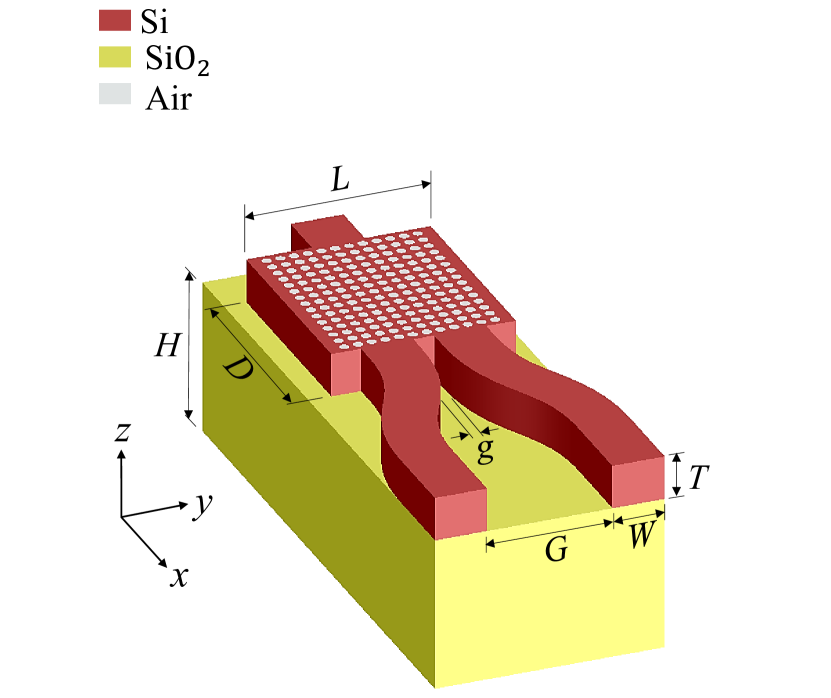
Fig. 2 represents the optimized structure by inverse design methos of PSO with a few circular air holes in silicon slab on a SiO2 substrate. The electromagnetic power distribution of TE00 incident polarization mode at cross section of the input waveguide has been depicted in the inset of Fig. 2.
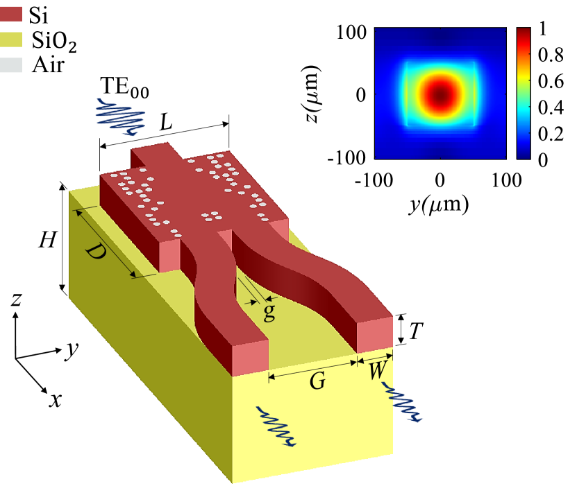
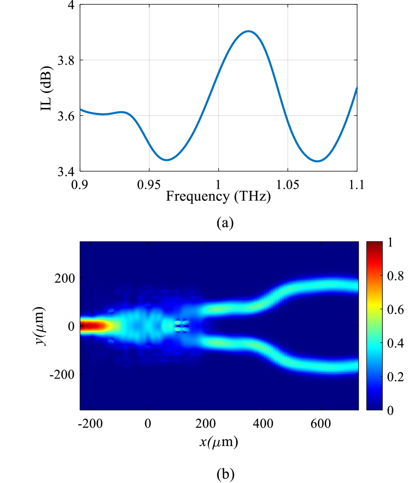
The air holes in the optimized structure act as scatterer points and based on interferences in the optimized region, constructive interferences take place and resulting in routing light to the output branches. Also, these holes make a photonic bandgap which prohibits THz waves to spread out in - direction; so light can only be guided in the output branches. The lack of holes in the optimized region creates a guiding electromagnetic modes in the bandgap which results in steering the light to the outputs. In Fig. 3, the simulation results for electromagnetic power distribution and IL of the optimized 50:50 TPS structure have been shown. As demonstrated in Fig. 3(a), the IL is less than 3.9 dB that correspond to the efficiency roughly 81% over the frequency range of 0.9–1.1 THz. Electromagnetic power distribution of the optimized TPS at the wavelength of 1.55 µm is shown in Fig. 3(b) which represents the route of light over the device.
In this letter, we have proposed a 50:50 TE TPS based on digitized metamaterials. The device contains an input and two silicon waveguide outputs. It was optimized using PSO inverse design method. The optimized device represented IL of less than 3.9 dB over the frequency range of 0.9–1.1 THz. It contains a few air holes in silicon slab which are deposited on SiO2 substrate. The advantages of the device contains compactness, efficient, small footprint, all-dielectric and compatible with CMOS fabrication technology. This device is a suitable candidate for high density THz circuits.
Acknowledgments This work was supported by MSIT(Ministry of Science and ICT), Korea, under the ICT Creative Consilience program(IITP-2020-2011-1-00783) supervised by the IITP(Institute for Information & communications Technology Planning & Evaluation).
References
- [1] P. H. Siegel, \JournalTitleIEEE transactions on microwave theory and techniques 52, 2438 (2004).
- [2] M.-A. Brun, F. Formanek, A. Yasuda, M. Sekine, N. Ando, and Y. Eishii, \JournalTitlePhysics in Medicine & Biology 55, 4615 (2010).
- [3] S. Smye, J. Chamberlain, A. Fitzgerald, and E. Berry, \JournalTitlePhysics in Medicine & Biology 46, R101 (2001).
- [4] S. Ergun and S. Sonmez, \JournalTitleJournal of Management and Information Science 3, 13 (2015).
- [5] Y. Cheng, Y. Wang, Y. Niu, and Z. Zhao, \JournalTitleOptics express 28, 6350 (2020).
- [6] T. Harter, C. Füllner, J. Kemal, S. Ummethala, J. Steinmann, M. Brosi, J. Hesler, E. Bründermann, A.-S. Müller, W. Freude et al., \JournalTitleNature Photonics 14, 601 (2020).
- [7] H. Sarieddeen, N. Saeed, T. Y. Al-Naffouri, and M.-S. Alouini, \JournalTitleIEEE Communications Magazine 58, 69 (2020).
- [8] V. Petrov, D. Moltchanov, Y. Koucheryavy, and J. M. Jornet, \JournalTitleIEEE Transactions on Vehicular Technology 69, 6822 (2020).
- [9] P. Han, X. Wang, and Y. Zhang, \JournalTitleAdvanced Optical Materials 8, 1900533 (2020).
- [10] J. A. Spies, J. Neu, U. T. Tayvah, M. D. Capobianco, B. Pattengale, S. Ostresh, and C. A. Schmuttenmaer, \JournalTitleThe Journal of Physical Chemistry C 124, 22335 (2020).
- [11] L. A. Sterczewski, J. Westberg, Y. Yang, D. Burghoff, J. Reno, Q. Hu, and G. Wysocki, \JournalTitleACS Photonics 7, 1082 (2020).
- [12] J. Huang, J. Li, Y. Yang, J. Li, Y. Zhang, J. Yao et al., \JournalTitleOptics express 28, 7018 (2020).
- [13] H. Xiong, Q. Ji, T. Bashir, and F. Yang, \JournalTitleOptics express 28, 13884 (2020).
- [14] J. Huang, J. Li, Y. Yang, J. Li, J. Li, Y. Zhang, and J. Yao, \JournalTitleOptics Express 28, 17832 (2020).
- [15] L. Yang and L. Jiu-Sheng, \JournalTitleJournal of the European Optical Society-Rapid Publications 13, 1 (2017).
- [16] B. S.-Y. Ung, C. Fumeaux, H. Lin, B. M. Fischer, B. W.-H. Ng, and D. Abbott, \JournalTitleOptics express 20, 4968 (2012).
- [17] C. C. Homes, G. L. Carr, R. P. Lobo, J. D. LaVeigne, and D. B. Tanner, \JournalTitleApplied optics 46, 7884 (2007).
- [18] K. S. Reichel, R. Mendis, and D. M. Mittleman, \JournalTitleScientific reports 6, 28925 (2016).
- [19] Y. Hou, F. Fan, X.-H. Wang, and S.-J. Chang, \JournalTitleOptik 124, 5285 (2013).
- [20] A. Jakhar, P. Kumar, A. Moudgil, V. Dhyani, and S. Das, \JournalTitleAdvanced Optical Materials 8, 1901714 (2020).
- [21] H.-T. Chen, W. J. Padilla, M. J. Cich, A. K. Azad, R. D. Averitt, and A. J. Taylor, \JournalTitleNature photonics 3, 148 (2009).
- [22] A. Jakhar, P. Kumar, S. Husain, V. Dhyani, and S. Das, \JournalTitleACS Applied Nano Materials 3, 10767 (2020).
- [23] H. Zeng, Y. Zhang, F. Lan, S. Liang, L. Wang, T. Song, T. Zhang, Z. Shi, Z. Yang, X. Kang et al., \JournalTitleIEEE Transactions on Terahertz Science and Technology 9, 491 (2019).
- [24] W. S. Lee, S. Nirantar, D. Headland, M. Bhaskaran, S. Sriram, C. Fumeaux, and W. Withayachumnankul, \JournalTitleAdvanced Optical Materials 6, 1700852 (2018).
- [25] C. W. Berry and M. Jarrahi, \JournalTitleJournal of Infrared, Millimeter, and Terahertz Waves 33, 127 (2012).