]
Stacking and gate tunable topological flat bands, gaps and anisotropic strip patterns in twisted trilayer graphene
Abstract
Trilayer graphene with a twisted middle layer has recently emerged as a new platform exhibiting correlated phases and superconductivity near its magic angle. A detailed characterization of its electronic structure in the parameter space of twist angle , interlayer potential difference , and top-bottom layer stacking reveals that flat bands with large Coulomb energy vs bandwidth are expected within a range of near and for top-bottom layer stacking, between a wider range for stacking, whose bands often have finite valley Chern numbers thanks to the opening of primary and secondary band gaps in the presence of a finite , and below for all considered. The largest ratios are expected at the magic angle when meV for AA, and slightly below near for finite meV for AB stackings, and near for both stackings. When is the saddle point stacking vector between AB and BA we observe pronounced anisotropic local density of states (LDOS) strip patterns with broken triangular rotational symmetry. We present optical conductivity calculations that reflect the changes in the electronic structure introduced by the stacking and gate tunable system parameters.
I Introduction
Research on the electronic structure of nearly flat bands in moire materials has seen a recent surge of interest following experimental observation of strongly correlated and localized Mott-like phases and superconductivity in magic angle twisted bilayer graphene (tBG) Kim et al. (2017); Cao et al. (2018a, b); Yankowitz et al. (2019); Cao et al. (2020) discussed by electronic structure studies Suárez Morell et al. (2010); Bistritzer and MacDonald (2011); Jung et al. (2014). Research interests in vertical van der Waals (vdW) heterojunctions Koma (1992, 1999); Geim and Grigorieva (2013) in search of strongly correlated flat bands have expanded beyond the twisted bilayer graphene Bistritzer and MacDonald (2011); Suárez Morell et al. (2010); Kim et al. (2017); Cao et al. (2018a, b); Yankowitz et al. (2019); Koshino et al. (2018); Cao et al. (2020); Leconte et al. (2019); Koshino and Son (2019), to include systems like twisted double bilayer graphene (tDBG) Chebrolu et al. (2019); Koshino (2019); Burg et al. (2019); Lee et al. (2019); Choi and Choi (2019), and various forms of twisted trilayer graphene Suárez Morell et al. (2013); Zuo et al. (2018); Ma et al. (2021); Mora et al. (2019); Tsai et al. (2019); Khalaf et al. (2019); Li et al. (2019); Carr et al. (2020); Szendrő et al. (2020); Shi et al. (2021a); Chen et al. (2021); Polshyn et al. (2020); Park et al. (2020); Lei et al. (2020); Wu et al. (2020); Călugăru et al. (2021a) including twisted monolayer-bilayer graphene (tMBG) Suárez Morell et al. (2013); Li et al. (2019); Szendrő et al. (2020); Carr et al. (2020); Ma et al. (2021); Shi et al. (2021a); Chen et al. (2021); Polshyn et al. (2020); Park et al. (2020); Lei et al. (2020); Wu et al. (2020). Unlike the systems with a single moire twist interface like tBG, tDBG, or tMBG, in twisted trilayer graphene with finite successive interlayer twist angles we have two interfaces giving rise to double moire patterns. When these moire patterns are mutually incommensurate they give rise to supermoire patterns Wang et al. (2019); Anđelković et al. (2020); Leconte and Jung (2020), also called moire of moire patterns Kerelsky et al. (2021); Zhu et al. (2020); Tsai et al. (2019) that can multiply the features in the electronic structure, while strongest double moire interference happen for commensurate patterns, exemplified by the large secondary band gaps in graphene encapsulated by hexagonal boron nitride Leconte and Jung (2020).
Commensurate double moire trilayer graphene with a middle layer twist Ma et al. (2021); Mora et al. (2019); Khalaf et al. (2019); Carr et al. (2020); Li et al. (2019); Lopez-Bezanilla and Lado (2020); Lei et al. (2020); Park et al. (2021); Hao et al. (2021); Călugăru et al. (2021a, b), called here simply twisted trilayer graphene (tTG), has emerged as a system of renewed interest thanks to the observation of moire flat band superconductivity with a critical temperature higher than tBG. Park et al. (2021); Hao et al. (2021); Cao et al. (2021) Earlier studies reported that the first magic-angle of tTG is larger by a factor than that of tBG Khalaf et al. (2019); Li et al. (2019); Carr et al. (2020) and it was shown tight-binding models that nearly flat bands accompany the linear dispersions at the point in the moire Brillouin zone (mBZ) that persists even when out-of-plane lattice relaxation and perpendicular electric fields are present Carr et al. (2020); Lopez-Bezanilla and Lado (2020). Other earlier work based on continuum models have analyzed the properties of tTG from various perspectives, including the band topology Ma et al. (2021), predominant metallic character Mora et al. (2019), hierarchy of magic angles Khalaf et al. (2019), symmetry analysis Călugăru et al. (2021b). It was noted that the band structures vary considerably depending on the relative stacking vector between top and bottom layers Li et al. (2019); Lei et al. (2020) that in the presence of out of plane relaxations and electric fields shows metallic bands for AA while a band gap opens for AB stackings Park et al. (2021); Hao et al. (2021). Due to the large parameter space of twist angles, electric fields and stacking possibilities earlier work have reported the electronic structure for select system parameters.
In this work we present new phase diagrams of the bandwidths and valley Chern numbers of the low energy nearly flat bands in the continuous parameter space of twist angles and the interlayer potential difference for different stacking vectors between top and bottom layers. Our detailed calculations show that it is possible to achieve nearly flat bands prone to strong correlations in a relatively wide range of twist angles around the magic angle and around in the presence of appropriate interlayer potential difference for AA top-bottom layer stacking, and in an even broader range if the top and bottom layers stacking is AB (or equivalently BA) where a finite can isolate the bands by opening primary and secondary gaps over a wide range or parameters often leading to finite valley Chern numbers. Additionally, we show the impact of stacking and electric fields in the local density of states (LDOS) maps that can be measured through scanning tunneling probes, and we present linear optical conductivity calculations for select stacking arrangements as a means to distinguish different electronic structures. Anisotropic moire patterns can be obtained for top-bottom layer sliding vectors that break the triangular rotational symmetry and the stripe patterns are maximized for the saddle point (SP) stacking vector suggesting that this type of stripe phases could be favored when the system is subject to uniaxial strains or to boundary conditions that alter the stacking dependent energy landscape.
Our manuscript is organized as follows. In Sec. II we introduce the model Hamiltonian, Sec. III is devoted to the discussion of the electronic band structures for different interlayer potential difference and stacking configurations, in Sec. IV we discuss the numerical results of effective Coulomb interaction for the two different stackings and the valley Chern numbers, in Sec. V we discuss the anisotropy of the LDOS for non-symmetric stackings, in Sec. VI we report the numerical results on the longitudinal linear optical conductivity, and in Sec VII we summarize our work.
II Model Hamiltonian
The Hamiltonian of tTG with twisted middle layer can be captured by twisting the top-bottom and middle layers in opposite senses. The continuum model Hamiltonian for the valley is
| (1) |
where = diag(, , 0, 0, , ) is a matrix that captures the interlayer potential difference due to an external electric field where we assume the interlayer potentials of at the top and bottom layers.
In our model, for the bottom (b), the middle (m), and the top (t) layers, represents a matrix describing a Dirac Hamiltonian rotated by which is given as
| (2) |
The system conventions are similar to that in Ref. Chebrolu et al. (2019) for tDBG and we use for the Fermi velocity m/s, which corresponds to an effective nearest neighbor hopping term of eV. Here is in general a rotation operator for spin and is the -component of the Pauli matrices. The interlayer tunneling at the interface is denoted as a matrix given by
| (3) |
where and , are given as , when the twist angle is small enough. Here, is equal to the length of one side of the first Brillouin zone of single layer of graphene where . The interlayer tunning matrix was first formulated for the local-AB-stacking in the twisted bilayer graphene system in Ref. Bistritzer and MacDonald (2011) and was generalized for other initial stackings dictated by in Ref. Jung et al. (2014) as
| (4) |
where and . Here, is a relative sliding of the top layer with respect to the bottom layer, and we define , and , resulting in
| (5) |
when for AA-stacking with . When for AB-stacking the matrix remains the same but acquires a phase factor as follows,
| (6) |
and when or, equivalently, for BA stacking the matrix is conjugate transposed. The interlayer tunneling elements use the polynomial parametrization of Ref. Chebrolu et al. (2019) relating inter- and intra-sublattice hopping terms where , , and that is fitted to the exact exchange and random phase approximation (EXX+RPA) interlayer energy minima and local density approximation (LDA) interlayer tunneling, and leads to different eV and eV when effective out of plane relaxations are considered. Equal tunneling parameters eV correspond to the rigid model in the absence of relaxations, which are consistent with the LDA values for the eV perpendicular interlayer tunneling term in an AB stacked bilayer Jung and MacDonald (2014).
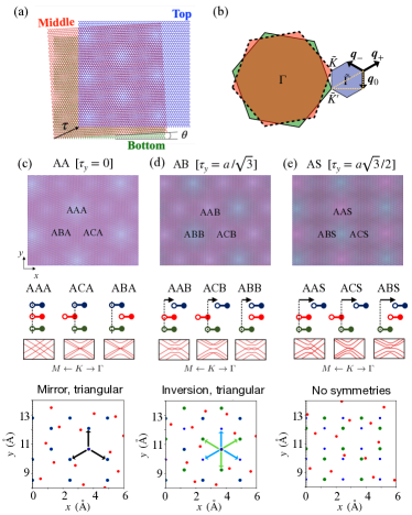
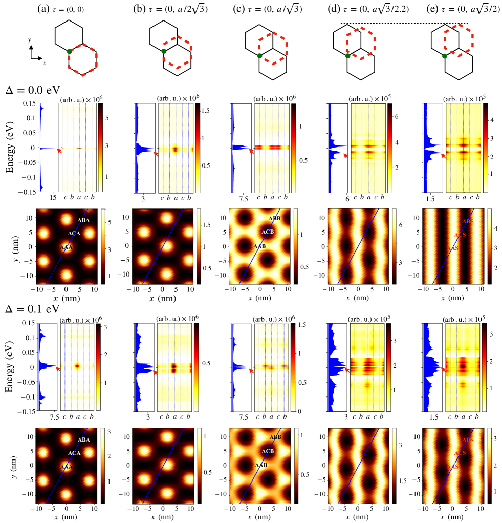
In tTG with aligned top and bottom layers we have two moire interfaces with the same moire length . The magic angle given as is enlarged with respect to the tBG value by a factor of following the renomalization of the interlayer tunneling strength when we decompose the interaction of the outer layers Dirac Hamiltonian with the middle layer Khalaf et al. (2019); Carr et al. (2020); Li et al. (2019). The top layer sliding vector with respect to bottom layer is a control knob that alters the electronic structure of our system. For most cases we choose where top and bottom layers are exactly on top of each other, where the top layer has a Bernal stacking-like displacement, and the intermediate saddle point stacking is chosen as the representative broken rotational symmetry system leading to clearest strip patterns. We interchangeably refer to the AA and AB stacking of the top-bottom layers in tTG with the sliding vectors and , see Fig. 1. The local AAB-stacking is generated by sliding the top layer by from the AAA-stacking where all three layers are exactly aligned on top of each other. Because the stacking sliding geometry of the middle layer does not alter the resulting band structure after it is twisted we use the bottom and top layer stacking labels to classify the different systems. When we twist the middle layer by the magic angle , see Fig. 1, we can identify two overlaid patterns with equal period nm where a finite introduces changes in the local stacking maps. The black letters represent on top of the moire patterns the local stacking geometries as shown schematically in the second row. The AA-tTG has mirror symmetry with respect to the middle layer as illustrated from the AAA, ABA, and BAB local stacking configurations, while mirror symmetry is broken in AB-tTG but an inversion center is present for all twist angles, preserving in both cases the triangular rotational symmetry of the moire patterns. All these symmetries are broken for intermediate vectors away from the symmetric stacking configurations, and this is illustrated for a large commensurate twist angle and three different top layer sliding vectors in the third row of Fig. 1.
III ENERGY BANDS
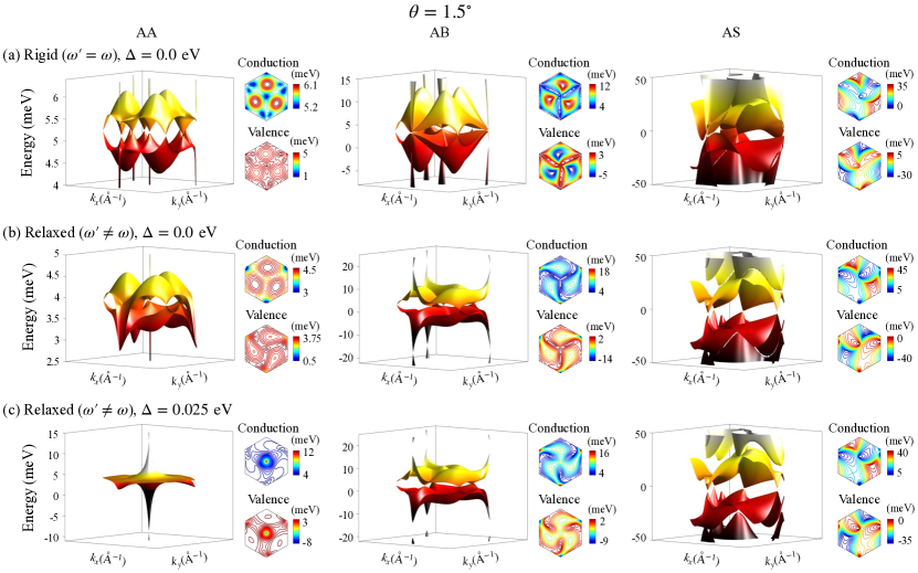
The electronic structure of tTG strongly depends on system parameters such as twist angle , the interlayer potential difference , and top layer sliding vector . Here, our bandwidth phase diagram analysis for tTG shows that in addition to the magic angle the narrowest are found for zero or moderate values of at a smaller twist angle near for , and near for , and for all considered and when . Sample electronic structure surface plots and contours are shown in Fig. 2 for near the magic angle and in Figs. 3 and 4 we present continuous sweep phase diagrams of electronic structure features in the parameter space of , and . In this work we focus our attention on systems with with eV and eV in Eq. (5) that accounts for out of plane relaxations that gaps the Dirac cones at for AA and at for AB.
We begin by illustrating in Fig. 2 the impact of the stacking type in the bandwidth corresponding to the valence and conduction low energy bands that give rise to the progressively increasing sequence meV, meV and meV as we depart from the initial stacking geometry for and show in the figures for . We will show that a finite interlayer potential difference alters the bandwidths giving rise to a roughly linear increase near the magic angle for AA and a non-monotonic behavior for AB and SP stackings. For the AA case a finite shifts the band touching point at to proportionally higher positive and negative energy values without opening a primary band gap nor secondary gaps in both the valence and conduction bandsCarr et al. (2020); Lopez-Bezanilla and Lado (2020), while for AB we have positive and gaps Park et al. (2021); Hao et al. (2021). The opening of the band gaps and subsequent isolations possible for AB systems leads to low energy bands with well defined valley Chern numbers depending on and values in contrast to AA bands that remain metallic.
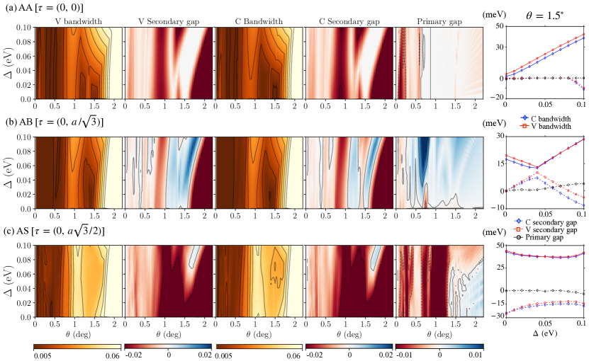
The bandwidth for conduction and valence bands and the associated primary gap and secondary gap for different system parameters are illustrated in Fig. 3 for continuous variations of and for select values, and for continuous for a fixed and select values in Fig. 4. The bandwidth phase diagrams and gaps are strongly affected by and the results in Fig. 3 shows that the electron hole asymmetry is generally weaker in our tTG models where we do not incorporate interactions with the substrate Shi et al. (2021b); Shin et al. (2021) nor the remote hopping terms included in a Bernal stacked bilayer graphene McCann and Fal’ko (2006); Jung and MacDonald (2014). This is manifested in the closely resembling behavior of the different , , phase diagrams for the conduction and valence bands. As we just noted, for we generally find metallic bands that have narrowest bandwidths near the magic angle , a slightly lower , and . The presence of interlayer potential differences introduces a mild almost linear increase in the bandwidths near that follows approximately the relation , indicating that narrowest bands are expected when there are no displacement electric fields. The bandwidths remain consistently narrow meV for all considered values of in the small twist angle regime when . The situation is different for where isolated bands can be found in the presence of a finite between a wider twist angles range and at islands near for sufficiently large , and near for all values of . The narrowest bandwidth regions are found in the vicinity of slightly below the magic angle and . A finite at shows a non-monotonic behavior in reducing the bandwidth with before it eventually recovers the almost linear relationship beyond eV where the secondary band gaps start to decrease. Similar to , the bandwidths remain consistently narrow meV for all considered values of when . Finally, for a third sliding vector corresponding to a saddle point stacking the bandwidths remain practically constant with a value on the order of 40 meV for twist angles between , while narrowest bandwidths are expected for small twist angles in the range of explored values to up to 0.1 eV like in the other configurations.
IV EFFECTIVE COULOMB INTERACTION and VALLEY CHERN NUMBERS
In this section we provide measures on the relative dominance of the Coulomb interaction energies versus the bandwidth by calculating the ratios of the bare Coulomb energy versus bandwidth, and the screened effective Coulomb energy versus bandwidth that provides a more reliable measure for the onset of gaps and insulating phases when the bands are not overlapping. Typically we consider to be in the strong correlation regime when these ratios are larger than 1. The effective screened Coulomb energy is given by Chebrolu et al. (2019)
| (7) |
where the moire length is given by . The effective screening Debye length is expressed as where is the two-dimensional DOS defined as
| (8) |
where is the Heaviside step function. Thus, is proportional to the bands overlap represented by negative gap values (). Here, is the area of a moire unit cell in real space, and we use for the dielectric constant of graphene.
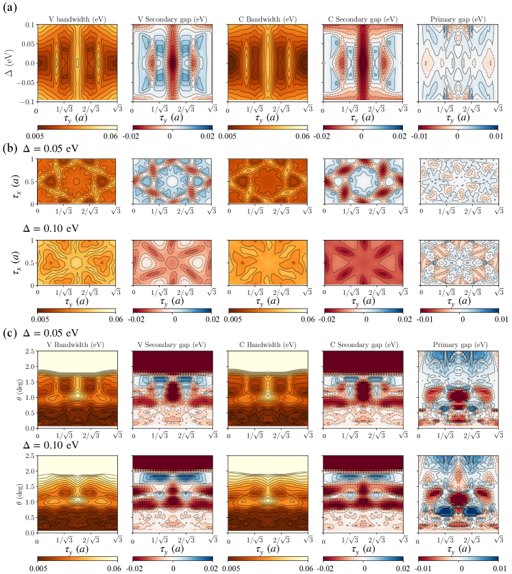
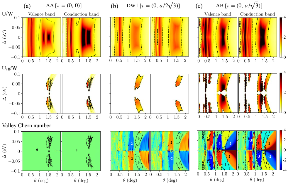
The first two rows in Fig. 5 show and as a function of twist angle and interlayer potential difference for the valence and conduction flat bands, which generally show a weak electron-hole asymmetry regardless of the different top-botoom layer sliding geometries considered, namely , the intermediate , and .
The first row showing plots resembles the bandwidth phase diagram in Fig. 3 manifesting a strong dependence with respect to . We indicate the contours of with black dotted lines to help distinguish the regions where we expect strong correlations. For the large Coulomb energy regions are found at the aforementioned bandwidth minima angles of and for angles below . Sliding to an intermediate stacking has the effect of reducing the overall strength of the ratio seen in , and further sliding until achieves a wider region of large ratios in the parameter space of and where peak maxima are shifted to a lower and for angles below . The second row showing includes suppression of the Coulomb energy due to screening effects proportional to the overlap of the flat bands with the neighboring bands. Similar to the first row, we indicate the contours of with black dotted lines. This quantity allows to define the regions where the bands are isolated and we have a higher likelihood of developing insulating gapped phases. For all stacking geometries considered we observe that twist angles around within can develop regions when we add a sufficiently large .
The valley Chern numbers corresponding to the flat bands are represented in the third row of Fig. 5 and they will be well defined when the band are not crossing each other. The valley Chern number of the energy band is defined as
| (9) |
where is the Berry curvature given by Ref. Xiao et al. (2010) as follows,
| (10) |
The valley Chern numbers of both the valence and the conduction low energy bands are shown in the lower row in Fig. 5. For they are found to be topologically trivial for finite electric fields and twist angles less than 2.5∘, while for twist angles larger than 3∘ the valley Chern numbers are not well-defined due to the strongly metallic character of the system (not shown). On the other hand, the valley Chern numbers of and cases show diverse topologically nontrivial phases. One general observation is that the valley Chern number signs can be reversed with the perpendicular electric field direction, and the valley Chern numbers of the valence and conduction bands are opposite to each other adding up to a zero sum. For we expect trivial Chern numbers for strong correlation regions for and finite , and valley Chern numbers for twist angles that are below and above in twist angle. For the parameter space of isolated bands and finite valley Chern numbers are expanded thanks to the easier opening of band gaps and . Near the magic angle the valley Chern numbers are finite , becoming for smaller angles, and becoming larger angles. The valley Chern numbers become again mostly trivial for the saddle point AS stacking with when the system behaves like a metal. Our calculations show that a variety of finite valley Chern numbers can be tailored depending on the specific top-bottom layer sliding configuration .
V LOCAL DENSITY OF STATES
We have just noted that the electronic structure undergo important changes depending on the sliding vector following variations of the real space moire patterns, which in turn impacts the local density of states (LDOS) associated to the nearly flat bands. Here we show that LDOS maxima locations in tTG follow closely the same rule of thumb applicable in tBG that concentrates the charge at the AA local stacking regions of a tBG interface. Because in tTG we have two tBG interfaces the AA local stacking centers at each interface will distribute in different manners depending on the vector, as we illustrate in Fig. 6 for five selected cases of top layer sliding in the -direction.
For the case the reinforced LDOS profiles at the AAA local stacking regions give rise to a triangular lattice much like what we find in tBG. The LDOS patterns progressively split into two displaced triangular lattices and thus breaks the triangular rotational symmetry as we introduce a small sliding in the top graphene layer by a vector along the -direction in Fig. 6(b). The triangular rotational symmetry is recovered for , see Fig. 6(c), and the LDOS maxima forming a honeycomb lattice consisting of AA local interfaces between bottom-middle and middle-top layers. When we continue sliding the top layer further the double moire pattern start forming stripe shapes for the LDOS in Fig. 6(d)(e) which break maximally the rotational symmetry at the so called saddle point . These LDOS charge anisotropy patterns in Fig. 6(d) and (e) resemble the scanning tunneling spectroscopy (STS) results in Ref. Zuo et al. (2018) of twisted trilayer graphene.
Application of a positive interlayer potential difference has the effect of redistributing the carrier densities of the valence bands towards the bottom-middle interface as it tends to lower the bottom layer energy following the definition in Eq. (1). Thus for the honeycomb pattern resulting from the stacking we see a brightened bottom-middle interface and dimmed middle-top interface upon application of . For similar reasons, a finite distorts the straight stripe patterns seen in Fig. 6(e) turning them into snake like shapes by populating the bottom interface and depleting the top interface charge densities near the respective AA stacking regions. In general an interlayer potential difference has the effect of broadening the DOS in energy pushing the states to higher energy values away from neutrality, and for the stacking case we see the opening of a band gap at charge neutrality from the DOS profile.
VI LONGITUDINAL OPTICAL CONDUCTIVITY
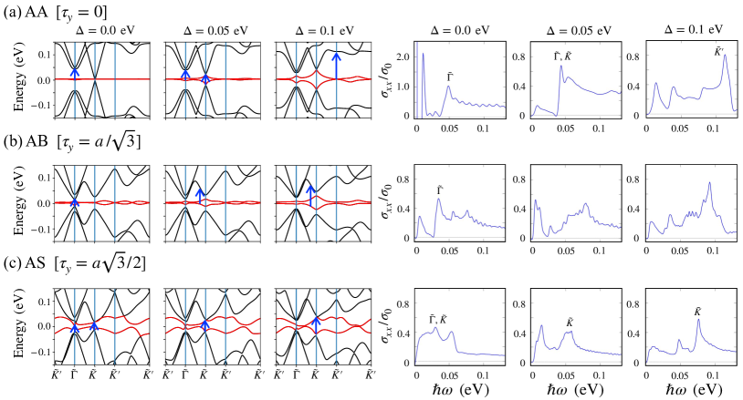
In this section, we present the numerical analysis of the longitudinal linear optical conductivity of tTG at the magic twist angle for select values of the displacement field for the three stacking arrangements , and in Figs. 7(a), (b), and (c), respectively. The real part of the longitudinal linear optical conductivity is given by Ando et al. (2002); Gusynin et al. (2006, 2007); Falkovsky and Varlamov (2007); Min and MacDonald (2009)
| (11) |
where is the general current operator, is the Fermi-Dirac distribution function, is the th eigen-energy at , and is the universal optical conductivity of the single layer of graphene.
In Fig. 7, we illustrate the energy bands for select band structures together with the real part of the linear optical conductivity at zero chemical potential. We have not considered the Drude term in order to present more clearly the contributions of interband optical transitions. In the band structure figures, the lowest electron- and hole-bands are highlighted by the red lines. The corresponding real part of the normalized linear optical conductivity in the longitudinal direction are juxtaposed together with the mBZ maps on the right panel. We stressed the prominent contributions in the conductivity denoted by the blue diamonds and investigated the locations of the optical transitions in the mBZ maps.
The locations of each transition peak in momentum space are also illustrated in the band structure figures by the blue arrows. For stacking cases, the largest contributions of the optical transitions occur at or points when the displacement fields are = , eV. On the other hand, the biggest portion of the transition takes place at when = eV. In stacking, the biggest contribution of the transitions happens at when = eV. On the other hand, the transitions mostly occur at an intermediate point away from the high-symmetry point for = , eV. For the -stacking case, the largest optical contributions are mostly coming from point and it is noteworthy that the contribution in the mBZ map is anisotropic, which reflects the triangular rotational symmetry in keeping with the anisotropic Fermi surface as well as the real-space stripe patterns.
VII SUMMARY
Trilayer graphene with middle layer twist (tTG) gives rise to the simplest form of commensurate double moire pattern formed by two twisted graphene interfaces and has become a new system of interest following recent observations of superconductivity with higher critical temperatures than in twisted bilayer graphene (tBG). We have presented a detailed electronic structure calculations and associated phase diagrams for the bandwidth, gaps and valley Chern numbers for continuous variations of the twist angle and interlayer potential difference for selected top-bottom layer sliding vectors. We have aimed at providing a more comprehensive description of the system behavior in a wider range of system parameters than in earlier work to predict new system parameters where strong correlations and finite valley Chern numbers are expected, and paid particular attention to the role of the interlayer sliding that can either preserve or break the triangular rotational symmetry to create anisotropic strip patterns. While the bandwidths of the low energy states generally follow the sequence they are modified by which alters the twist angle dependent bandwidth phase diagram. Our calculations predict narrowest bandwidths on the order of 10 meV around and in the limit of small for stacking, and around for stacking. Application of a finite generally widens the bandwidth of the low energy flat bands and in the case of the low energy bands can be isolated to generate finite valley Chern numbers in a wide range of twist angles and interlayer potential difference . We have also analyzed the impact of stacking and electric fields in the local density of states (LDOS) maps that can be measured through scanning tunneling probes, and showed that the anisotropic stripe patterns can be maximized when the top-bottom layers have a saddle point stacking geometry. The specific stacking vector favored in the system might be modifiable through different device preparation conditions, for example in the presence of strains introduced by boundary condition stresses, that would in turn lead to observable changes in charge transport or through optical experiments. The linear optical conductivity calculations we have carried out provide information about the changes expected in the interband transition peaks that can be introduced by varying the system parameters and suggests its usefulness as a system characterization tool.
Acknowledgements.
We gratefully acknowledge Y. J. Park’s help in the preparation of some figures. This work was supported by Samsung Science and Technology Foundation under project no. SSTF-BA1802-06 for J. S., the Korean National Research Foundation grants NRF-2020R1A2C3009142 for B. L. C., and NRF-2020R1A5A1016518 for J. J. We acknowledge computational support from KISTI through Grant KSC-2020-CRE-0072.Appendix. Band structures for select cases
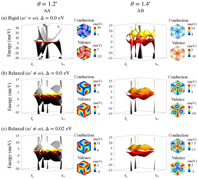
In this appendix we additionally present in Fig. 8 the band structures for the cases of having the local minima in the conduction and valence bandwidths for and in addition to the case that we showed in Fig. 3(a) and (b). When the top and the bottom layers have a relative displacement by , the valence bandwidth at has the local minimum meV, and the conduction bandwidth at has the local minimum meV. For the top-bottom layer displacement , both valence and conduction bandwidths have the local minima meV at . The corresponding band structures for the rigid ( eV), the out-of-plane relaxed lattice ( eV and eV), and with finite displacement field eV are shown on the left (right) column for () in Fig.8(a), (b), and (c), respectively. We note that unequal interlayer tunneling helps to flatten the low energy bands by reducing the band dispersion at the moire Brillouin zone corners.
References
- Kim et al. (2017) K. Kim, A. DaSilva, S. Huang, B. Fallahazad, S. Larentis, T. Taniguchi, K. Watanabe, B. J. LeRoy, A. H. MacDonald, and E. Tutuc, PNAS 114, 3364 (2017).
- Cao et al. (2018a) Y. Cao, V. Fatemi, S. Fang, K. Watanabe, T. Taniguchi, E. Kaxiras, and P. Jarillo-Herrero, Nature 556, 43 (2018a).
- Cao et al. (2018b) Y. Cao, V. Fatemi, A. Demir, S. Fang, S. L. Tomarken, J. Y. Luo, J. D. Sanchez-Yamagishi, K. Watanabe, T. Taniguchi, E. Kaxiras, R. C. Ashoori, and P. Jarillo-Herrero, Nature 556, 80 (2018b).
- Yankowitz et al. (2019) M. Yankowitz, S. Chen, H. Polshyn, Y. Zhang, K. Watanabe, T. Taniguchi, D. Graf, A. F. Young, and C. R. Dean, Science 363, 1059 (2019).
- Cao et al. (2020) Y. Cao, D. Rodan-Legrain, O. Rubies-Bigorda, J. M. Park, K. Watanabe, T. Taniguchi, and P. Jarillo-Herrero, Nature 583, 215 (2020).
- Suárez Morell et al. (2010) E. Suárez Morell, J. D. Correa, P. Vargas, M. Pacheco, and Z. Barticevic, Phys. Rev. B 82, 121407 (2010).
- Bistritzer and MacDonald (2011) R. Bistritzer and A. H. MacDonald, PNAS 108, 12233 (2011).
- Jung et al. (2014) J. Jung, A. Raoux, Z. Qiao, and A. H. MacDonald, Phys. Rev. B 89, 205414 (2014).
- Koma (1992) A. Koma, Thin Solid Films 216, 72 (1992).
- Koma (1999) A. Koma, J. Cryst. Growth 201-202, 236 (1999).
- Geim and Grigorieva (2013) A. K. Geim and I. V. Grigorieva, Nature 499, 419 (2013).
- Koshino et al. (2018) M. Koshino, N. F. Yuan, T. Koretsune, M. Ochi, K. Kuroki, and L. Fu, Phys. Rev. X 8, 031087 (2018).
- Leconte et al. (2019) N. Leconte, S. Javvaji, J. An, and J. Jung, arXiv:1910.12805 (2019).
- Koshino and Son (2019) M. Koshino and Y.-W. Son, Phys. Rev. B 100, 075416 (2019).
- Chebrolu et al. (2019) N. R. Chebrolu, B. L. Chittari, and J. Jung, Phys. Rev. B 99, 235417 (2019).
- Koshino (2019) M. Koshino, Phys. Rev. B 99, 235406 (2019).
- Burg et al. (2019) G. W. Burg, J. Zhu, T. Taniguchi, K. Watanabe, A. H. MacDonald, and E. Tutuc, Phys. Rev. Lett. 123, 197702 (2019).
- Lee et al. (2019) J. Y. Lee, E. Khalaf, S. Liu, X. Liu, Z. Hao, P. Kim, and A. Vishwanath, Nat. Commun. 10, 5333 (2019).
- Choi and Choi (2019) Y. W. Choi and H. J. Choi, Phys. Rev. B 100, 201402 (2019).
- Suárez Morell et al. (2013) E. Suárez Morell, M. Pacheco, L. Chico, and L. Brey, Phys. Rev. B 87, 125414 (2013).
- Zuo et al. (2018) W.-J. Zuo, J.-B. Qiao, D.-L. Ma, L.-J. Yin, G. Sun, J.-Y. Zhang, L.-Y. Guan, and L. He, Phys. Rev. B 97, 035440 (2018).
- Ma et al. (2021) Z. Ma, S. Li, Y.-W. Zheng, M.-M. Xiao, H. Jiang, J.-H. Gao, and X. Xie, Science Bulletin 66, 18 (2021).
- Mora et al. (2019) C. Mora, N. Regnault, and B. A. Bernevig, Phys. Rev. Lett. 123, 026402 (2019).
- Tsai et al. (2019) K.-T. Tsai, X. Zhang, Z. Zhu, Y. Luo, S. Carr, M. Luskin, E. Kaxiras, and K. Wang, arXiv:1912.03375 , 2 (2019).
- Khalaf et al. (2019) E. Khalaf, A. J. Kruchkov, G. Tarnopolsky, and A. Vishwanath, Phys. Rev. B 100, 085109 (2019).
- Li et al. (2019) X. Li, F. Wu, and A. H. MacDonald, arXiv:1907.12338 (2019).
- Carr et al. (2020) S. Carr, C. Li, Z. Zhu, E. Kaxiras, S. Sachdev, and A. Kruchkov, Nano Lett. 20, 3030 (2020).
- Szendrő et al. (2020) M. Szendrő, P. Süle, G. Dobrik, and L. Tapasztó, “Ultra-flat twisted superlattices in 2d heterostructures,” (2020), arXiv:2001.11462 [cond-mat.mes-hall] .
- Shi et al. (2021a) Y. Shi, S. Xu, M. M. A. Ezzi, N. Balakrishnan, A. Garcia-Ruiz, B. Tsim, C. Mullan, J. Barrier, N. Xin, B. A. Piot, T. Taniguchi, K. Watanabe, A. Carvalho, A. Mishchenko, A. K. Geim, V. I. Fal’ko, S. Adam, A. H. C. Neto, and K. S. Novoselov, Nat. Phys. (2021a), 10.1038/s41567-021-01172-9.
- Chen et al. (2021) S. Chen, M. He, Y.-H. Zhang, V. Hsieh, Z. Fei, K. Watanabe, T. Taniguchi, D. H. Cobden, X. Xu, C. R. Dean, and M. Yankowitz, Nat. Phys. (2021), 10.1038/s41567-020-01062-6.
- Polshyn et al. (2020) H. Polshyn, J. Zhu, M. A. Kumar, Y. Zhang, F. Yang, C. L. Tschirhart, M. Serlin, K. Watanabe, T. Taniguchi, A. H. MacDonald, and A. F. Young, Nature 588, 66 (2020).
- Park et al. (2020) Y. Park, B. L. Chittari, and J. Jung, Phys. Rev. B 102, 035411 (2020).
- Lei et al. (2020) C. Lei, L. Linhart, W. Qin, F. Libisch, and A. H. MacDonald, “Mirror symmetry breaking and stacking-shift dependence in twisted trilayer graphene,” (2020).
- Wu et al. (2020) Z. Wu, Z. Zhan, and S. Yuan, arXiv:2012.13741 (2020).
- Călugăru et al. (2021a) D. Călugăru, F. Xie, Z.-D. Song, B. Lian, N. Regnault, and B. A. Bernevig, arXiv:2102.06201 (2021a).
- Wang et al. (2019) Z. Wang, Y. B. Wang, J. Yin, E. Tóvári, Y. Yang, L. Lin, M. Holwill, J. Birkbeck, D. J. Perello, S. Xu, J. Zultak, R. V. Gorbachev, A. V. Kretinin, T. Taniguchi, K. Watanabe, S. V. Morozov, M. Anđelković, S. P. Milovanović, L. Covaci, F. M. Peeters, A. Mishchenko, A. K. Geim, K. S. Novoselov, V. I. Fal’ko, A. Knothe, and C. R. Woods, Science Advances 5, eaay8897 (2019).
- Anđelković et al. (2020) M. Anđelković, S. P. Milovanović, L. Covaci, and F. M. Peeters, Nano Letters 20, 979 (2020).
- Leconte and Jung (2020) N. Leconte and J. Jung, 2D Materials 7, 031005 (2020).
- Kerelsky et al. (2021) A. Kerelsky, C. Rubio-Verdú, L. Xian, D. M. Kennes, D. Halbertal, N. Finney, L. Song, S. Turkel, L. Wang, K. Watanabe, T. Taniguchi, J. Hone, C. Dean, D. N. Basov, A. Rubio, and A. N. Pasupathy, Proceedings of the National Academy of Sciences 118 (2021), 10.1073/pnas.2017366118, https://www.pnas.org/content/118/4/e2017366118.full.pdf .
- Zhu et al. (2020) Z. Zhu, P. Cazeaux, M. Luskin, and E. Kaxiras, Phys. Rev. B 101, 224107 (2020).
- Lopez-Bezanilla and Lado (2020) A. Lopez-Bezanilla and J. L. Lado, Phys. Rev. Research 2, 033357 (2020).
- Park et al. (2021) J. M. Park, Y. Cao, K. Watanabe, T. Taniguchi, and P. Jarillo-Herrero, Nature 590, 249 (2021).
- Hao et al. (2021) Z. Hao, A. M. Zimmerman, P. Ledwith, E. Khalaf, D. H. Najafabadi, K. Watanabe, T. Taniguchi, A. Vishwanath, and P. Kim, Science 371, 1133 (2021).
- Călugăru et al. (2021b) D. Călugăru, F. Xie, Z.-D. Song, B. Lian, N. Regnault, and B. A. Bernevig, (2021b), arXiv:2102.06201 [cond-mat.str-el] .
- Cao et al. (2021) Y. Cao, J. M. Park, K. Watanabe, T. Taniguchi, and P. Jarillo-Herrero, (2021), arXiv:2103.12083 [cond-mat.mes-hall] .
- Jung and MacDonald (2014) J. Jung and A. H. MacDonald, Phys. Rev. B 89, 035405 (2014).
- Shi et al. (2021b) J. Shi, J. Zhu, and A. H. MacDonald, Phys. Rev. B 103, 075122 (2021b).
- Shin et al. (2021) J. Shin, Y. Park, B. L. Chittari, J.-H. Sun, and J. Jung, Phys. Rev. B 103, 075423 (2021).
- McCann and Fal’ko (2006) E. McCann and V. I. Fal’ko, Phys. Rev. Lett. 96, 086805 (2006).
- Xiao et al. (2010) D. Xiao, M.-C. Chang, and Q. Niu, Rev. Mod. Phys. 82, 1959 (2010).
- Ando et al. (2002) T. Ando, Y. Zheng, and H. Suzuura, Journal of the Physical Society of Japan 71, 1318 (2002).
- Gusynin et al. (2006) V. Gusynin, S. Sharapov, and J. Carbotte, Physical review letters 96, 256802 (2006).
- Gusynin et al. (2007) V. Gusynin, S. Sharapov, and J. Carbotte, Physical review letters 98, 157402 (2007).
- Falkovsky and Varlamov (2007) L. Falkovsky and A. Varlamov, The European Physical Journal B 56, 281 (2007).
- Min and MacDonald (2009) H. Min and A. H. MacDonald, Phys. Rev. Lett. 103, 067402 (2009).