Superconducting \ceV3Si for quantum circuit applications
Abstract
\ceV3Si thin films are known to be superconducting with transition temperatures up to , depending on the annealing temperature and the properties of the substrate underneath. Here we investigate the film structural properties with the prospect of further integration in silicon technology for quantum circuits. Two challenges have been identified: (i) the large difference in thermal expansion rate between \ceV3Si and the Si substrate leads to large thermal strains after thermal processing, and (ii) the undesired silicide phase \ceVSi2 forms when \ceV3Si is deposited on silicon. The first of these is studied by depositing layers of \ceV3Si on wafers of sapphire and oxidized silicon, neither of which react with the silicide. These samples are then heated and cooled between room temperature and , during which in-situ XRD measurements are performed. Analysis reveals a highly non-linear stress development during heating with contributions from crystallization and subsequent grain growth, as well as the thermal expansion mismatch between silicide and substrate, while the film behaves thermoelastically during cooling. The second challenge is explored by depositing films of 20, 50, 100 and of \ceV3Si on bulk silicon. For each thickness, six samples are prepared, which are then annealed at temperatures between 500 and , followed by measurements of their resistivity, residual resistance ratio and superconducting critical temperature. A process window is identified for silicide thicknesses of at least , within which a trade-off needs to be made between the quality of the \ceV3Si film and its consumption by the formation of \ceVSi2.
I Introduction
Quantum technologies based on solid state matter are now spreading from academic laboratories to the most advanced semiconductor foundries [1, 2]. Among the materials to be integrated, superconducting thin films are of major interest as they are part of many quantum architectures. For instance, such films can be used to manipulate, read and couple superconducting or spin qubits with the use of superconducting resonators [3, 4], are developed for non-dissipative interconnections or can even be part of the quantum device itself when integrated as source and drain contacts of CMOS transistors. Since silicon technology is by far the most advanced method of nanofabrication, it is important to identify superconducting materials that are fully compatible with such an environment. Among these, silicides appears as the most suitable materials [5, 6], and as \ceV3Si has the highest known critical temperature of any silicide known so far [7, 8], it is a prime candidate for these applications. In working towards integration of \ceV3Si, two key problems have been identified: (i) a reduction in the superconducting critical temperature due to increased thermal strain after annealing [9], and (ii) the formation of the non-superconducting phase \ceVSi2 at the interface with a silicon channel or substrate.
In systems where reservoirs of both Si and V are available, the undesired phase \ceVSi2 is expected to form, which is both the first phase to nucleate [10] and is thermodynamically favored [11]. This rules out the self-aligned silicide (SALICIDE) process for the formation of the desired \ceV3Si, in which pure metal is deposited on exposed silicon contacts. Instead, it has motivated the adoption of \ceV3Si sputtering from compound targets [12, 13], after which an annealing step is required to trigger the crystallization. This thermal processing leads to the build-up of strain in the final silicide film, which is known to negatively affect its critical temperature [14, 15, 16, 17, 18, 19]. Earlier work has shown that this strain depends strongly on the mismatch in thermal expansion coefficient (TEC) between the silicide and the substrate, and can lead to a suppression in superconducting critical temperature by on silicon [9]. Section II provides a detailed analysis of the impact of crystallization, grain growth and thermal expansion mismatch on the strongly temperature-dependent development of stress in \ceV3Si thin films.
Besides causing the buildup of large tensile stresses, thermal processing of \ceV3Si on silicon substrates also leads to the formation of \ceVSi2. The presence of \ceVSi2 at the interface between the superconducting \ceV3Si and the Si substrate may not be a problem per se. It is imperative, however, that a layer of \ceV3Si with a thickness on the order of its superconducting coherence length remains. The simultaneous formation of the two silicide phases after the deposition of amorphous \ceV3Si on bulk silicon wafers is discussed in section III. We find that when or less of \ceV3Si is deposited, no superconductivity is observed after crystallization annealing. For layers of 100 or , the superconducting critical temperature of the film is found to initially improve with annealing temperature, until at some point superconductivity disappears when all \ceV3Si is consumed by a growing layer of \ceVSi2.
II In-situ XRD analysis
Sputtering a \ceV3Si target leads to the deposition of an amorphous layer of the desired intermetallic compound which presents superconductivity at temperatures of around , far below that of the crystalline form (measured but not shown). In order to nucleate the crystalline \ceV3Si phase, heat has to be applied. During the experiment described in the present section, the \ceV3Si was isolated from any potential element (V and Si especially) that would affect the crystallization phenomenon. Thus, depositing the intermetallic compound on oxides (silica and sapphire) offers the possibility to study the isolated film by itself, affected by the substrate only mechanically. The evolution of the stresses in the \ceV3Si film as a function of the annealing temperature was monitored by in-situ X-ray diffraction (XRD) using a Smartlab Rigaku X-ray diffractometer equipped with a copper (Cu \ceK_α) source, a punctual detector and a DHS 1100 Anton Paar furnace using a nitrogen atmosphere at a pressure slightly above ambient, i.e. , to avoid atmospheric contamination.
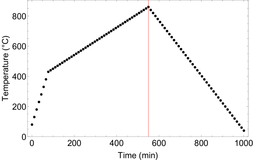
Layers of \ceV3Si were deposited on two types of substrates: oxidized silicon with a thick surface oxide, and sapphire. Both in-plane and out-of-plane XRD measurements were performed on different samples of each substrate. For both measurements, a parallel slit analyzer with an angular aperture of for out-of-plane measurement and for in-plane ones, is positioned in front of the detector in order to be insensitive to peak shift due to the radial displacement of the sample induced by thermal expansion of the sample holder. This way, the observed peak shift is only related to a real d-spacing variation. For both measurements, – scans around the \ceV3Si (210) close to were performed. Profiles were acquired while heating the samples from up to and then during cooling from to room temperature. The temperature profile versus time is given in Fig. 1.
Peak fitting was performed with the HighScore Plus software from PANalytical, from which the d-spacing and the integral breadth of the \ceV3Si (210) peak were considered. The \ceV3Si crystallization followed by in-situ XRD is shown as a contour map for the out-of-plane measurements in Fig. 2 and the in-plane measurements in Fig. 3.
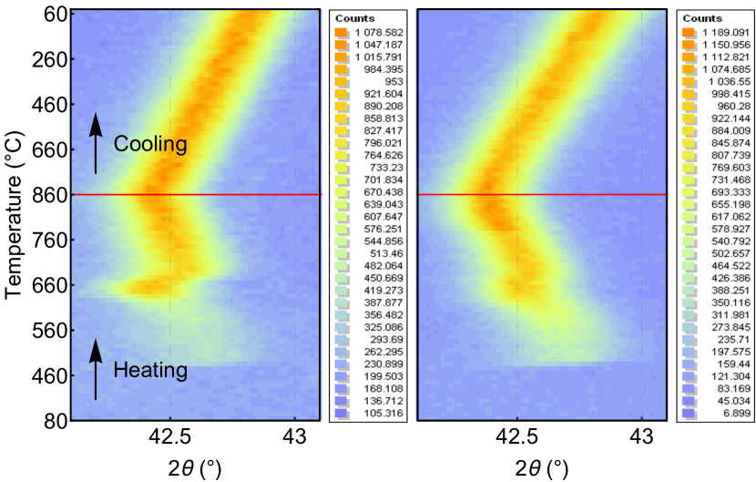
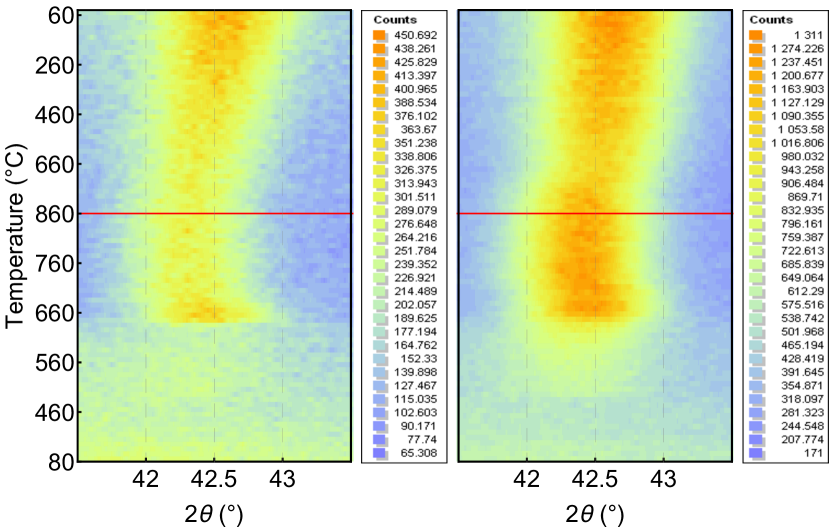
During heating, for both substrates, a characteristic peak of (210) \ceV3Si is observed above , which marks the crystallization temperature of the as-deposited amorphous \ceV3Si layer. One can thus deduce that the nucleation temperature of \ceV3Si crystalline phase is close to 500 °C. From in-plane and out-of-plane peak positions, one can extract the stress and the temperature-dependent stress-free lattice parameter of the layer. Assuming a bi-axial state of stress in the layer, it can be deduced following the methodology [20],
| (1) |
where is the in-plane bi-axial state of stress, and are the strain and the -spacing along the direction , respectively, is the stress-free -spacing and is the angle between the considered direction and the normal to the surface. and are the X-ray Elastic Constants (XEC) for the hkl plane considered. The XEC can be easily calculated [21] by knowing the single-crystal elastic constants of the \ceV3Si structure [22]. For the (210) plane, using the arithmetic average of the Voigt and Reuss XEC, known as the Neerfeld limit, we found and . The in-plane stress is then given by [20]
| (2) |
and the stress-free -spacing, , by
| (3) |
In Fig. 4a, the stress evolution deduced from this analysis is plotted versus the annealing temperature for both types of substrate. In both cases, the initial stress at crystallization is highly tensile, around . This is in agreement with the expected volume shrinkage that occurs during the crystallization, assuming that the density of the amorphous phase is smaller than the density of the crystalline phase. This tensile stress is then partially relaxed.
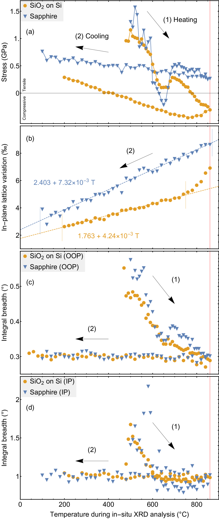
In Fig. 4c,d the integral breadth (IB) evolution of the (210) peak vs annealing temperature is plotted, which can be correlated to the crystallite size through the Scherrer equation [23, 24]. This figure shows that the IB is high at the crystallization temperature and then goes down with increasing temperature, a behavior that is similar for the in-plane and out-of-plane directions, and can be interpreted as a crystallite size increase. However, one should note that the in-plane and and out-of-plane setup was different and can not be compared directly.
Indeed, for the in-plane setup, the IB decreased down to 1° at 650°C and stayed constant during further annealing. This value of 1° is the instrumental width given by a silicon reference powder, which implies that the in-plane crystallite size is very large above and can no longer be estimated from IB broadening. As we observe an increase of the crystallite size out of plane up to , we may assume that the lateral crystallite size also continues to grow up to this temperature. In the case of the out-of-plane measurements, the setup was more accurate, and the estimated crystallite size is about for the highest annealing temperature. It can clearly be concluded that there is a strong anisotropy in grain size on both substrates. On both substrates, the in-plane IB stabilizes at due to saturation of the instrument resolution, while the detected out-of-plane crystallite size increases continuously to the maximum temperature of the experiment.
During cooling, the stress evolution exhibits a linear behavior, in agreement with a pure thermoelastic stress induced by the TEC mismatch between the film and the substrate. This is confirmed by looking at the in-plane lattice parameter evolution with temperature (Fig 4b). The behavior is linear as expected, but more interestingly, the slope of these straight lines is and for the sapphire and Si substrate respectively, in good agreement with the in-plane TEC of (0001) sapphire ( in the temperature range 300–) [25], and with the TEC of Si ( in the temperature range 200–) [26]. From the stress-free lattice parameter extraction, we calculated a TEC of the \ceV3Si phase of . The TEC mismatch between the film and the substrate should therefore have added a tensile stress to the stress measured at , in agreement with the observation in Fig. 4a. As expected, since the TEC mismatch is larger with the Si substrate than with the sapphire, the tensile stress increases faster on Si than on sapphire. Extrapolating this thermoelastic behavior to the device operating temperature (i.e. a few K), a stress level of is obtained for \ceV3Si on sapphire and for \ceV3Si on silicon. Of course these values depend on the initial residual stress before cooling, and thus on the thermal budget applied to the samples. Since the slow cooling occurred entirely thermoelastically and followed the TEC of the substrate, it is not expected that the rate of cooling has any impact on the final stress obtained. The difference in room-temperature strain between this report and those found in earlier experiments where in-situ XRD analysis was performed up to [9] is thus attributed to differences in the maximum temperature that was reached.
III Competition between \ceV3Si and \ceVSi2 formation
A second set of experiments was performed to study the stability of the superconducting \ceV3Si phase on a silicon substrate. After sputter deposition of \ceV3Si on a silicon substrate, an intermixing layer of Si and V can be expected to form where the atomic concentration of vanadium ranges from zero in the substrate to within the deposited layer. Above this mixed zone, the precise matching of the deposited atomic ratio to the stoichiometry of \ceV3Si will prevent the formation of \ceVSi2. Within the mixed zone however, \ceVSi2 nucleation is likely to occur. Since this mixed zone is interfaced from below by pure silicon, and from above by \ceV3Si, its disappearance or consumption by \ceV3Si formation would require that V move upwards while leaving progressively purified Si behind. Such movement is prevented by the chemical potential, as the thermodynamically stable state in the presence of excess silicon is for the vanadium to be bound in \ceVSi2 [11]. Furthermore, even if a V reservoir were present in the form of a super-stoichiometric vanadium concentration (i.e. above 75%) in the deposited layer, it is unlikely that the mixed zone would be consumed by \ceV3Si formation. Since silicon is the dominant diffusing species in \ceVSi2 and at the V/Si interface, with diffusion rates of two orders of magnitude higher than that of V in \ceV3Si [27, 28], any part of the intermixing layer with lower vanadium concentration than that of \ceV3Si is expected to quickly extend downward and decrease in V content due to upward Si diffusion, preventing \ceV3Si growth and aiding the formation of \ceVSi2.
Once \ceVSi2 and \ceV3Si are both present, competition will arise between the further growth of either silicide. While \ceV3Si (\ceV_0.75Si_0.25) has a larger effective heat of formation (EHF) from pure V and Si per mole of atoms involved in total [11], the energy gain per vanadium atom is greater for \ceVSi2 (\ceV_0.33Si_0.67), of which three times as many molecules can be formed for a fixed amount of vanadium. When \ceV3Si interfaces with silicon, it is therefore energetically favorable for the following reaction to occur (EHF indicated below),
| (4) |
where an energy of is gained per mole of \ceV3Si that is transformed. Scanning electron microscope (SEM) images of the growth of the \ceVSi2 phase during thermal processing are shown in Fig. 5.
To study this interplay, a different set of samples was prepared in addition to those discussed in section II. Layers with thicknesses of 20, 50, 100 and of \ceV3Si were deposited onto (100)-oriented silicon wafers from a compound \ceV3Si target using RF magnetron sputtering equipment. This target had a measured silicon content of between (WDXRF) and (supplier data), which could further differ from the final Si content in the deposited layer by [13]. These wafers were cleaned with hydrofluoric acid (HF) before entering the sputtering chamber. Smaller pieces of were then annealed during 2 minutes in a Jipelec furnace with a ramp rate. For each thickness of \ceV3Si, six different samples were thermally processed at temperatures between 500 and , as indicated in Fig. 6. These samples were then characterized by measuring their room-temperature sheet resistance (corrected for their shape and size by calculating the sheet resistance ratio of multiple unannealed wafer-sized and samples), and by following the resistance of smaller samples during slow cooling to cryogenic temperatures of in order to extract both the superconducting critical temperature and the residual resistance ratio (RRR).
At , the resistivity of the thinner layers (20, 50 and ) was found to be comparable to that of as-deposited amorphous \ceV3Si (), while it exceeded this value by multiple orders of magnitude for the thicker layer of (out of range for our instruments), as shown in Fig. 6a. For all thicknesses, the resistivity then decreased with annealing temperature, to values below that measured for a reference sample with \ceV3Si on non-reacting sapphire annealed at (, indicated as a red dashed line). Since this reference value is the lowest resistivity that we have found for any layer of crystallized \ceV3Si, in a sample where we confirmed by XRD measurements that no other vanadium-rich compound was formed, we take any value lower than this on silicon substrates to indicate the presence of \ceVSi2. The formation of \ceVSi2 was confirmed by XRD analysis and identified at the Si/\ceV3Si interface by SEM imaging (see Fig. 5, bottom).
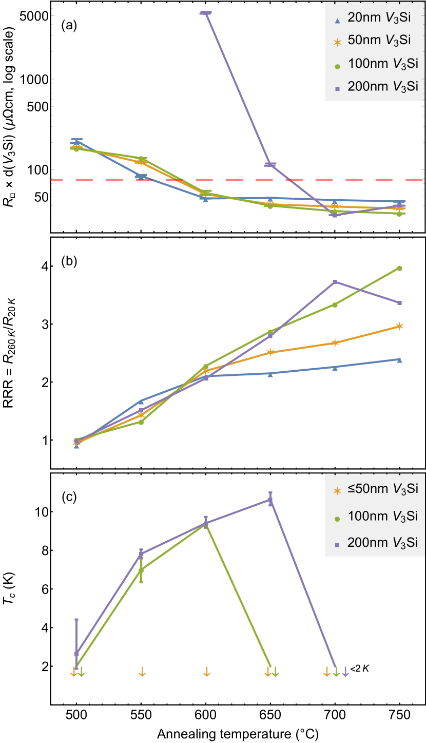
Smaller samples of were then wire bonded for four-point resistance measurements during both cooling and heating between 300 and in a Physical Properties Measurement System (PPMS). The residual resistance ratio of each sample was calculated as the ratio between the resistances at and , shown in Fig. 6b. This ratio gives insight into the material properties of the silicide layer since the resistance at low temperatures is dominated by impurity and defect scattering [29]. For higher annealing temperatures the RRR is greater for thicker layers (with the exception of the sample annealed at , which is also an outlier in terms of resistivity), which is consistent with the lower quality of thinner films as reported before [12]. After annealing at , however, we find that the RRR is highest in samples where only of \ceV3Si was deposited, followed by and , in that order. This could be an indication that a nearly homogeneous \ceVSi2 layer has already started to form at the \ceV3Si/Si interface in the thinnest of these films, with inhomogeneity increasing for thicker films of 50 and . Complete homogenization of a film during two minutes would suggest however that Si, the dominant diffusing species in \ceVSi2 formation [27], has diffused with a diffusivity of at least , values that have only been reported for annealing temperatures of [30]. The higher RRR at of the sample with deposited \ceV3Si suggests that this layer is too thick for diffusion to have already caused mixing throughout the entire film, and this relatively high value could be attributed to crystallization of \ceV3Si.
The appearance of crystalline \ceV3Si at temperatures of around is consistent with the in-situ XRD analysis on non-reactive substrates discussed in section II (see especially Fig. 2). This is further corroborated by the appearance of superconductivity with critical temperatures above as shown in Fig. 6c, to be contrasted with the critical temperature of of amorphous -thick \ceV3Si layers on silicon substrates prepared under identical conditions [9]. A critical temperature of (10% and 90% transitions at 10.32 and , respectively) was attained after annealing at in a deposited film, identical to that obtained on samples where \ceVSi2 formation was prevented by a film of \ceSiO2, with a superconducting transition that is only 12% wider [9]. This suggests that the nearby formation of \ceVSi2 does not have a significant impact on the superconducting properties of the remaining \ceV3Si. Meanwhile, the absence of superconductivity above in samples with 20 or deposited \ceV3Si, after annealing at any temperature, confirms that Si diffusion and \ceVSi2 formation rapidly remove \ceV3Si or even prevent its crystallization altogether in thinner films.
IV Discussion
Instead of forming vanadium silicide by reactive diffusion, \ceV3Si was directly sputtered from a compound target at the right stoichiometry, giving the advantages of having a sharp interface between the deposited layer and the substrate, and requiring no solid-state reaction to reach the desired phase. However, the interface must be better controlled in terms of impurities, and the \ceV3Si is amorphous after deposition. First, the crystallization was studied on 2 types of substrate, oxidized silicon with a thick \ceSiO2 surface layer and monocrystalline sapphire (\ceAl2O3). It was clear that no reaction occurred with either of these substrates at any temperature. Earlier work showed that the mismatch in TEC with the substrates strongly impacts the stress built up during the growth of \ceV3Si, which can lower the superconducting critical temperature [9].
Layer crystallization started at , leading to high tensile stress on either substrate up to . This stress then relaxed with increasing temperature, both due to atomic diffusion and the relatively low TEC of the substrates. From to around , an increase in tensile stress together with a decrease in the out-of-plane IB can be explained by grain growth in fair agreement with the model of P. Chaudari [31]. During cooling, the \ceV3Si stress behavior matches perfectly with TEC of silicon and sapphire substrate, indicating a purely thermoelastic behavior. It is thus clear that the thermomechanical properties of the substrate strongly impact the stress development in the \ceV3Si film, which can be mitigated by proper choice of annealing conditions.
Since \ceV3Si is amorphous after deposition, crystallization by subsequent thermal processing is required to achieve the desired superconducting properties. However, on a silicon substrate this has the undesired side effect of \ceVSi2 nucleation. In fact, in the thinnest films that were studied, with 20 and of deposited silicide, a nearly homogeneous \ceVSi2 layer had already started to form at the interface with the substrate before any crystallization of \ceV3Si was observed by critical temperature measurements. Full consumption of the deposited \ceV3Si occurred at higher temperatures between 600– and 650– for layers of 100 and , respectively, allowing for \ceV3Si crystallization, as well as grain growth. The critical temperatures thus obtained on a silicon substrate prior to complete \ceV3Si consumption are identical, within experimental error, to those obtained on \ceSiO2 [9], indicating no detrimental effect of diminished thickness or proximity to growing \ceVSi2 on the quality of the superconductor. This is in contrast with earlier results obtained by \ceV3Si sputtering from a compound target on heated Si substrates with of thermal \ceSiO2, where a strong dependence of film thickness was found below [12]. This variation in thickness was at the time attributed to the presence of impurities such as oxygen, while earlier reports had argued that the chemical composition of the layer was unimportant, and any variations that it causes in are due to a change in lattice parameter [14]. Since no reaction with the substrate occurs on \ceSiO2 (see Fig. 5), and the critical temperature is independent of the thickness of crystalline \ceV3Si itself, the reduced reported in this earlier study [12] could also be attributed to differences in grain growth, or stress development during cooling from , at which the layers were deposited, to cryogenic temperatures in the range of 10–.
V Conclusion
Superconducting thin films are of increasing interest as solid-state quantum technologies are scaled up. To facilitate large-scale fabrication, as well as co-integration with classical electronics, it is important that the choice of superconducting material is compatible with CMOS technology. This report addresses two challenges for the integration of \ceV3Si, which as a silicide with a superconducting critical temperature of up to [7, 8] is a natural candidate in this context.
The first is the reduction in critical temperature due to thermal strain. While \ceV3Si is compatible with the oxides of silicon and aluminum, both currently used in VLSI devices, it is necessary to mitigate the stresses induced by the interplay between crystallization, grain growth and TEC mismatch with the substrate. It is found that the final stress obtained on either substrate depends strongly on the thermal budget that the samples are subjected to, identifying annealing as a key process step to control the critical temperature of the film.
Second, thermal processing also provides a means of controlling the formation of the undesired phase \ceVSi2 on HF-cleaned silicon substrates. For \ceV3Si films with a thickness of or more, there exists a process window where it can be crystallized before consumption by the \ceVSi2 phase, with a temperature range that depends on the thickness of the film.
Direct applications of \ceV3Si could be in high-frequency resonators on oxides or oxidized substrates, where the impact of a potential stress residual on the quality factor has to be evaluated. A further interest would be to fabricate Josephson junctions, where the weak link could either be an oxide in a vertical geometry, or silicon in a planar junction. In the latter case, a Josephson field effect transistor could be fabricated by forming \ceV3Si in the source and drain contacts of a CMOS transistor, in which case one is faced with a trade-off between improving the \ceV3Si critical temperature and limiting the growth of the \ceVSi2 phase.
VI Data availability
The data that support the findings of this study are available from the corresponding author upon reasonable request.
VII Acknowledgments
T.D.V. acknowledges the European Union’s Horizon 2020 research and innovation programme under the Marie Skłodowska-Curie grant agreement No 754303. This work was partially supported by the ANR project SUNISiDEUP (ANR-19-CE47-0010). JX Nippon are gratefully acknowledged for providing the \ceV3Si deposition target.
References
- Arute et al. [2019] F. Arute, K. Arya, R. Babbush, D. Bacon, J. C. Bardin, R. Barends, R. Biswas, S. Boixo, F. G. Brandao, D. A. Buell, et al., “Quantum supremacy using a programmable superconducting processor,” Nature 574, 505–510 (2019).
- Zwerver et al. [2021] A. Zwerver, T. Krähenmann, T. Watson, L. Lampert, H. George, R. Pillarisetty, S. Bojarski, P. Amin, S. Amitonov, J. Boter, et al., “Qubits made by advanced semiconductor manufacturing,” arXiv preprint arXiv:2101.12650 (2021).
- Majer et al. [2007] J. Majer, J. Chow, J. Gambetta, J. Koch, B. Johnson, J. Schreier, L. Frunzio, D. Schuster, A. A. Houck, A. Wallraff, et al., “Coupling superconducting qubits via a cavity bus,” Nature 449, 443–447 (2007).
- Mi et al. [2018] X. Mi, M. Benito, S. Putz, D. M. Zajac, J. M. Taylor, G. Burkard, and J. R. Petta, “A coherent spin–photon interface in silicon,” Nature 555, 599–603 (2018).
- Shibata et al. [1981] T. Shibata, K. Hieda, M. Sato, M. Konaka, R. Dang, and H. Iizuka, “An optimally designed process for submicron mosfets,” in 1981 International Electron Devices Meeting (IEEE, 1981) pp. 647–650.
- Zhang and Zhang [2014] S.-L. Zhang and Z. Zhang, “Metal silicides in advanced complementary metal-oxide-semiconductor (cmos) technology,” in Metallic Films for Electronic, Optical and Magnetic Applications, edited by K. Barmak and K. Coffey (Woodhead Publishing, 2014) pp. 244–301.
- Hardy and Hulm [1953] G. F. Hardy and J. K. Hulm, “Superconducting silicides and germanides,” Physical Review 89, 884 (1953).
- Blumberg et al. [1960] W. Blumberg, J. Eisinger, V. Jaccarino, and B. Matthias, “Correlations between superconductivity and nuclear magnetic resonance properties,” Physical Review Letters 5, 149 (1960).
- Vethaak et al. [2021] T. D. Vethaak, F. Gustavo, T. Farjot, T. Kubart, P. Gergaud, S.-L. Zhang, F. Nemouchi, and F. Lefloch, “Influence of substrate-induced thermal stress on the superconducting properties of v 3 si thin films,” Journal of Applied Physics 129, 105104 (2021).
- Kräutle, Nicolet, and Mayer [1974] H. Kräutle, M.-A. Nicolet, and J. Mayer, “Kinetics of silicide formation by thin films of v on si and \ceSiO2 substrates,” Journal of Applied Physics 45, 3304–3308 (1974).
- Pretorius, Marais, and Theron [1993] R. Pretorius, T. Marais, and C. Theron, “Thin film compound phase formation sequence: An effective heat of formation model,” Materials Science Reports 10, 1–83 (1993).
- Michikami and Takenaka [1982] O. Michikami and H. Takenaka, “\ceV3Si thin-film synthesis by magnetron sputtering,” Japanese Journal of Applied Physics 21, L149 (1982).
- Theuerer and Hauser [1964] H. C. Theuerer and J. Hauser, “Getter sputtering for the preparation of thin films of superconducting elements and compounds,” Journal of Applied Physics 35, 554–555 (1964).
- Testardi et al. [1970] L. Testardi, J. Kunzler, H. Levinstein, and J. Wernick, “Unusual strain dependence of tc and related effects in a-15 superconductors,” Solid State Communications 8, 907–911 (1970).
- Testardi [1971] L. Testardi, “Unusual strain dependence of t c and related effects for high-temperature (a- 15-structure) superconductors: Sound velocity at the superconducting phase transition,” Physical Review B 3, 95 (1971).
- Testardi et al. [1971] L. Testardi, J. Kunzler, H. Levinstein, J. Maita, and J. Wernick, “Unusual strain dependence of tc and related effects for high-temperature (a-15-structure) superconductors: Elastic, thermal, and alloy behavior,” Physical Review B 3, 107 (1971).
- Testardi [1972] L. Testardi, “Structural instability, anharmonicity, and high-temperature superconductivity in a- 15-structure compounds,” Physical Review B 5, 4342 (1972).
- Batterman and Barrett [1964] B. Batterman and C. Barrett, “Crystal structure of superconducting \ceV3Si,” Physical Review Letters 13, 390 (1964).
- Batterman and Barrett [1966] B. Batterman and C. Barrett, “Low-temperature structural transformation in \ceV3Si,” Physical Review 145, 296 (1966).
- Noyan and Cohen [2013] I. C. Noyan and J. B. Cohen, Residual stress: measurement by diffraction and interpretation (Springer, 2013).
- Murray [2013] C. E. Murray, “Equivalence of kröner and weighted voigt-reuss models for x-ray stress determination,” Journal of Applied Physics 113, 153509 (2013).
- Gaillac, Pullumbi, and Coudert [2016] R. Gaillac, P. Pullumbi, and F.-X. Coudert, “Elate: an open-source online application for analysis and visualization of elastic tensors,” Journal of Physics: Condensed Matter 28, 275201 (2016), http://progs.coudert.name/elate/mp?query=mp-2567.
- Scherrer [1918] P. Scherrer, “Nachrichten von der gesellschaft der wissenschaften zu göttingen,” Mathematisch-Physikalische Klasse 2, 98–100 (1918).
- Cullity and Stock [2013] B. Cullity and S. Stock, Elements of x-ray diffraction (Pearson Education Limited, 2013).
- Vodenitcharova et al. [2006] T. Vodenitcharova, L. Zhang, I. Zarudi, Y. Yin, H. Domyo, and T. Ho, “The effect of thermal shocks on the stresses in a sapphire wafer,” IEEE transactions on semiconductor manufacturing 19, 449–454 (2006).
- Watanabe, Yamada, and Okaji [2004] H. Watanabe, N. Yamada, and M. Okaji, “Linear thermal expansion coefficient of silicon from 293 to 1000 k,” International journal of thermophysics 25, 221–236 (2004).
- Chu et al. [1974] W. Chu, H. Kraütle, J. Mayer, H. Müller, M.-A. Nicolet, and K. Tu, “Identification of the dominant diffusing species in silicide formation,” Applied Physics Letters 25, 454–457 (1974).
- Schutz and Testardi [1979] R. Schutz and L. Testardi, “The formation of vanadium silicides at thin-film interfaces,” Journal of Applied Physics 50, 5773–5781 (1979).
- Testardi, Poate, and Levinstein [1977] L. Testardi, J. Poate, and H. Levinstein, “Anomalous electrical resistivity and defects in a-15 compounds,” Physical Review B 15, 2570 (1977).
- Tu, Ziegler, and Kircher [1973] K. Tu, J. Ziegler, and C. Kircher, “Formation of vanadium silicides by the interactions of v with bare and oxidized si wafers,” Applied Physics Letters 23, 493–495 (1973).
- Chaudhari [1972] P. Chaudhari, “Grain growth and stress relief in thin films,” Journal of Vacuum Science and technology 9, 520–522 (1972).