Bright single photon emitters with enhanced quantum efficiency in a two-dimensional semiconductor coupled with dielectric nano-antennas
Bright single photon emitters with enhanced quantum efficiency in a two-dimensional semiconductor coupled with dielectric nano-antennas
Luca Sortino Panaiot G. Zotev Catherine L. Phillips Alistair J. Brash Javier Cambiasso Elena Marensi A. Mark Fox Stefan A. Maier Riccardo Sapienza Alexander I. Tartakovskii
Single photon emitters in atomically-thin semiconductors can be deterministically positioned using strain induced by underlying nano-structures. Here, we couple monolayer WSe2 to high-refractive-index gallium phosphide dielectric nano-antennas providing both optical enhancement and monolayer deformation. For single photon emitters formed on such nano-antennas, we find very low (femto-Joule) saturation pulse energies and up to 104 times brighter photoluminescence than in WSe2 placed on low-refractive-index SiO2 pillars. We show that the key to these observations is the increase on average by a factor of 5 in the quantum efficiency of the emitters coupled to the nano-antennas. This further allowed us to gain new insights into their photoluminescence dynamics, revealing the roles of the dark exciton reservoir and Auger processes. We also find that the coherence time of such emitters is limited by intrinsic dephasing processes. Our work establishes dielectric nano-antennas as a platform for high-efficiency quantum light generation in monolayer semiconductors.
Introduction
Single photon emitters (SPEs) in two-dimensional (2D) semiconducting WSe2 [1, 2, 3, 4, 5] open attractive perspectives for few-atom-thick devices for quantum technologies owing to favourable excitonic properties [6] and the integration with arbitrary substrates, including nano-structured surfaces [2, 6]. Several theoretical models have been proposed to provide insight into the origin of SPEs observed in the cryogenic photoluminescence (PL) spectra of 2D WSe2 [9, 10, 11, 12]. Their occurrence was explained by the presence of strain-induced potential traps for excitons [9], momentum-dark states [10] or various types of defects [11, 12]. While the exact origin is still under debate, first significant steps have been made to integrate WSe2 SPEs in devices, including electroluminescent structures [13, 14, 15], waveguides [16, 17] and tunable high-Q microcavities [18].
An appealing approach for the scalable and controllable fabrication of SPEs in WSe2 is the use of strain engineering for their deterministic positioning. Based on this idea, SiO2 [4] or polymer nano-pillars [20] have been employed to induce arrays of SPEs in atomically thin WSe2. In a similar approach, nano-structures made of noble metals were also employed where, due to the enhancement of the near-field intensity by plasmonic resonances, increased spontaneous emission rates were demonstrated [8]. However, plasmonic nano-antennas are known for large non-radiative losses, particularly detrimental for quantum technology applications. Thus, special care needs to be taken to separate SPEs from metallic surfaces with a dielectric spacer, which on the other hand will reduce the desired near-field coupling [8].
In contrast, the high-refractive-index dielectric materials used in our work offer a lossless alternative to metals [22]. Sub-wavelength dielectric nano-antennas exhibit optical Mie resonances carrying both electric and magnetic responses [23]. High-index dielectric nano-antennas have also been recently shown to provide an efficient approach for the enhancement of light-matter interaction as well as improved emitted light directionality in molecules [24], colloidal quantum dots [25] and excitons in 2D semiconductors [2, 26].
Here, we realise SPEs by placing monolayer WSe2 on top of dielectric nano-antennas made from high-refractive index GaP. Such SPEs show considerably enhanced PL counts per unit excitation power compared with previously reported emitters in WSe2 as well as the SPEs realised on low-index SiO2 nano-pillars in our work. The nano-antennas act as broadband optical cavities and also create strain pockets where the SPEs form. For such SPEs, our numerical simulations predict PL enhancement factors [2, 1] up to 800, compared with a more standard realisation of WSe2 SPEs on SiO2 pillars [4]. However, owing to the substantially enhanced quantum efficiency () in the SPEs on GaP nano-antennas, we can employ low excitation powers below fJ per laser pulse for their efficient operation. Thus, when we compare SPEs on GaP nano-antennas and SiO2 pillars experimentally, we find up to 104 brighter PL per unit laser power in the former system. We show that this substantial improvement in operation of the SPEs is related to the low of the SPEs on SiO2, 4 2 on average, compared with 21 3 average and up to 86 maximum in SPEs on GaP nano-antennas. For the latter we find that for the pumping laser repetition rate of 80 MHz, the SPE generates an effective single photons rate as high as 69 MHz under laser pulse energies around a fJ, corresponding to single photon rate of 5.5 MHz at the first lens.
Our approach allows further insight in the exciton dynamics in the hybrid 2D/0D system (2D monolayer/SPE) at very low excitation densities. We observe that as the pumping power is increased, exciton-exciton annihilation [28, 29], in our case of dark excitons, prevents efficient population of SPEs. This insight allows to develop a fuller understanding of the limitations of the low systems, in our case the SPEs on SiO2. There, the requirement for increased pumping power leads to a fast non-radiative depletion of excitons in 2D WSe2 and eventually results in a low single photon generation rate, that cannot be overcome by further increasing the pumping power. Our results thus highlight that the high-refractive-index nano-antennas, exhibiting near-field optical enhancement, provide strong advantages for producing bright SPEs in WSe2 monolayers.
Results
Optical properties of WSe2 SPEs positioned on GaP nano-antennas.
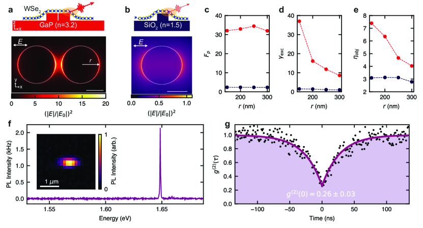
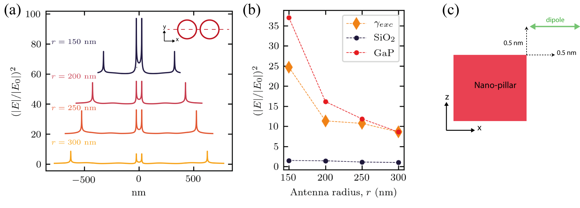
We use GaP nano-antennas composed of two closely spaced nano-pillars (Fig.1a), referred to as ‘dimer’ below (see also Supplementary Fig.1a). They exhibit an enhancement of the electromagnetic near-field intensity, as a result of the high refractive index () and the hybridization of the optical resonances of each individual pillars (see Supplementary Notes I & II). This is demonstrated in Fig.1a, where we show the calculated electric field intensity of the scattered radiation, , normalized by the intensity of the normally incident plane wave with linear polarization along the axis connecting the centres of the nano-pillars. The profile in Fig.1a corresponds to the top surface of the GaP dimer ( nm) having individual pillar radii of 150 nm. The enhancement of compared with exceeds 10 times and is particularly pronounced in the gap between the pillars [30, 24, 2]. The field is also strongly enhanced at the outer edges of the dimer where we expect SPEs to be located, as discussed further below and in Supplementary Note I. As shown in Fig.1b, under the same excitation conditions, a SiO2 nano-pillar ( nm, nm) does not show strong electromagnetic resonances, as a consequence of its low refractive index ().
A dipole emitter, such as an exciton in an SPE, spectrally and spatially overlapping with the near-field of the antenna, is expected to exhibit an enhanced light emission intensity [1]. This is a result of the product of the three main factors giving rise to the PL enhancement factor [2, 1]. Depending on the relative position and orientation of its dipole moment, the emitter experiences an increased local density of states and thus an enhanced spontaneous emission rate [31] via the Purcell effect, introducing a factor , directly improving the overall quantum efficiency, , where and are the rates of the radiative and non-radiative decay, respectively. In the absence of the Purcell effect =1 and we assumed . The antenna also modifies the dipole far field emission pattern, leading to an increased light collection efficiency above the antenna () within the given numerical aperture (NA) of the objective lens used in the detection system. Finally, the enhanced absorption of light in the material coupled to the antenna (in our case, a monolayer WSe2), quantified by the excitation rate proportional to the intensity of the local near-field, (Fig.1a-b), should in principle lead to a more efficient excitation of an SPE.
As shown in Fig.1c-e, we carried out numerical simulations (see Methods and Supplementary Note I) to extract the values of these three parameters for a dipole emitting at nm coupled to either GaP dimer nano-antennas (data in red) or to SiO2 nano-pillars (dark blue). The dipole is placed at the edge of the dimers, where the interaction is maximized [2], and is aligned perpendicularly to the edge of the nano-pillar (Supplementary Fig.1). For the dimers with the radii above 200 nm, the field enhancement at the outer edges is comparable to that in the gap (Supplementary Fig.1a). As shown in Fig.1c-e, a GaP nano-antenna may induce an enhancement of the PL intensity by at least two orders of magnitude [30, 24, 2], compared to SiO2 nano-pillars, as a consequence of the increase in both the spontaneous emission rate (Fig.1c), the excitation rate (Fig.1d), and a relatively modest effect in the collection efficiency (Fig.1e), as expected from the similar geometries of dimers and single pillars.
We note, that due to the high refractive index, for GaP most of the emitted light is directed downwards into the substrate, allowing only about 10 or less to be collected in the first lens (see further details in Supplementary Note 1). The highest single photon rate of 69 MHz, which we quote in this work, corresponds to the total number of photons emitted by the SPE, whereas in the experiments reported below we measure only up to 5.5 MHz generation rate at the first lens.
In order to experimentally examine these effects, we transferred WSe2 monolayers on top of an array of GaP nano-antennas (see Methods and Supplementary Note III) and on SiO2 nano-pillars as a reference (see Supplementary Note IV). With this approach, we achieve localized strain in the monolayer, introduced by the underlying nano-structure [6], which promotes the occurrence of localized SPEs at cryogenic temperatures. We find that the SPEs are formed on nearly all nano-antennas with the yield above 90, in agreement with previous reports [20, 4]. For some nano-antennas we find multiple emitters (see Supplementary Note III).
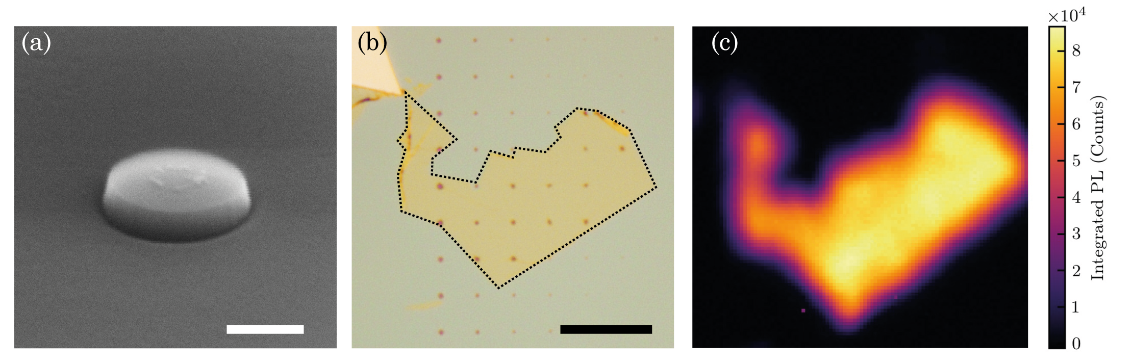
The samples are placed in a gas exchange cryostat, at a temperature of K, and excited (unless stated otherwise) with a non-resonant pulsed laser at 638 nm with 90 ps pulse width and a variable repetition rate. The laser excites below the GaP bandgap and is absorbed only by the WSe2 monolayer. The inset in Fig.1f shows a map of the integrated PL intensity from a WSe2 monolayer deposited on top of a GaP dimer nano-antenna ( nm). The PL signal exhibits a strong localization at the nano-antenna position, with negligible emission from the surrounding area where the unstrained WSe2 monolayer is positioned. As shown in Fig.1f, we observe bright and narrow PL lines, with suppressed background PL from the band of localized states in WSe2 as is usually observed when WSe2 is deposited on SiO2 pillars (Supplementary Fig.7a). We demonstrate the single-photon operation of the localized emitters in photon correlation measurements (see Methods). Fig.1g shows the second order correlation function, , for the emitter shown in Fig.1f, excited at nm, approximately 35 meV below the WSe2 A-exciton resonance. The pronounced anti-bunching behavior at zero time delay exhibits , confirming the non-classical photon emission statistics. In Supplementary Note V, we further correlate the SPEs emission energy to the strain induced in the 2D layer by the nano-antennas. Stretching of the WSe2 monolayer results in a progressively larger red-shift of the SPE emission when deposited on nano-antennas with smaller radii [6]. This behavior, analogous to the red-shift of WSe2 excitons under tensile deformation [6], confirms the impact of strain on the confinement potential and emission energy of WSe2 SPEs.
The position of the SPE and the orientation of the emitter dipole relative to the nano-antenna are important factors for the PL enhancement [2]. We expect that the SPEs will tend to form naturally around the edges of the nano-pillars (Fig.1a), where both the tensile strain and photonic enhancement is maximized as follows from our previously reported theoretical and experimental results (see Ref.[6] and Supplementary Note V). In these outer edge positions, the SPEs still experience strong enhancement of the electric field, which for the nano-pillars with the radii above 200 nm is comparable with the enhancement in the gap between the pillars (see Supplementary Fig.1a).
In our experiments (not reported here), we find that WSe2 SPEs on planar SiO2 have comparable PL intensities and lifetimes to those formed on SiO2 pillars, with the latter having the advantage of controlled positioning. Furthermore, we did not observe SPEs of reliably measurable PL intensity on planar GaP, where we find that overall PL of WSe2 is quenched as seen for example in Fig.1f. In what follows we focus on GaP dimer nano-antennas, as these provide pronounced and interesting photonic effects, as was shown in our preliminary work [2, 6]. On the other hand, less studied GaP monomers (single nano-pillars) may also be useful for achieving SPE positioning and improved PL in WSe2 monolayers. This may be a subject of another investigation beyond our current work.
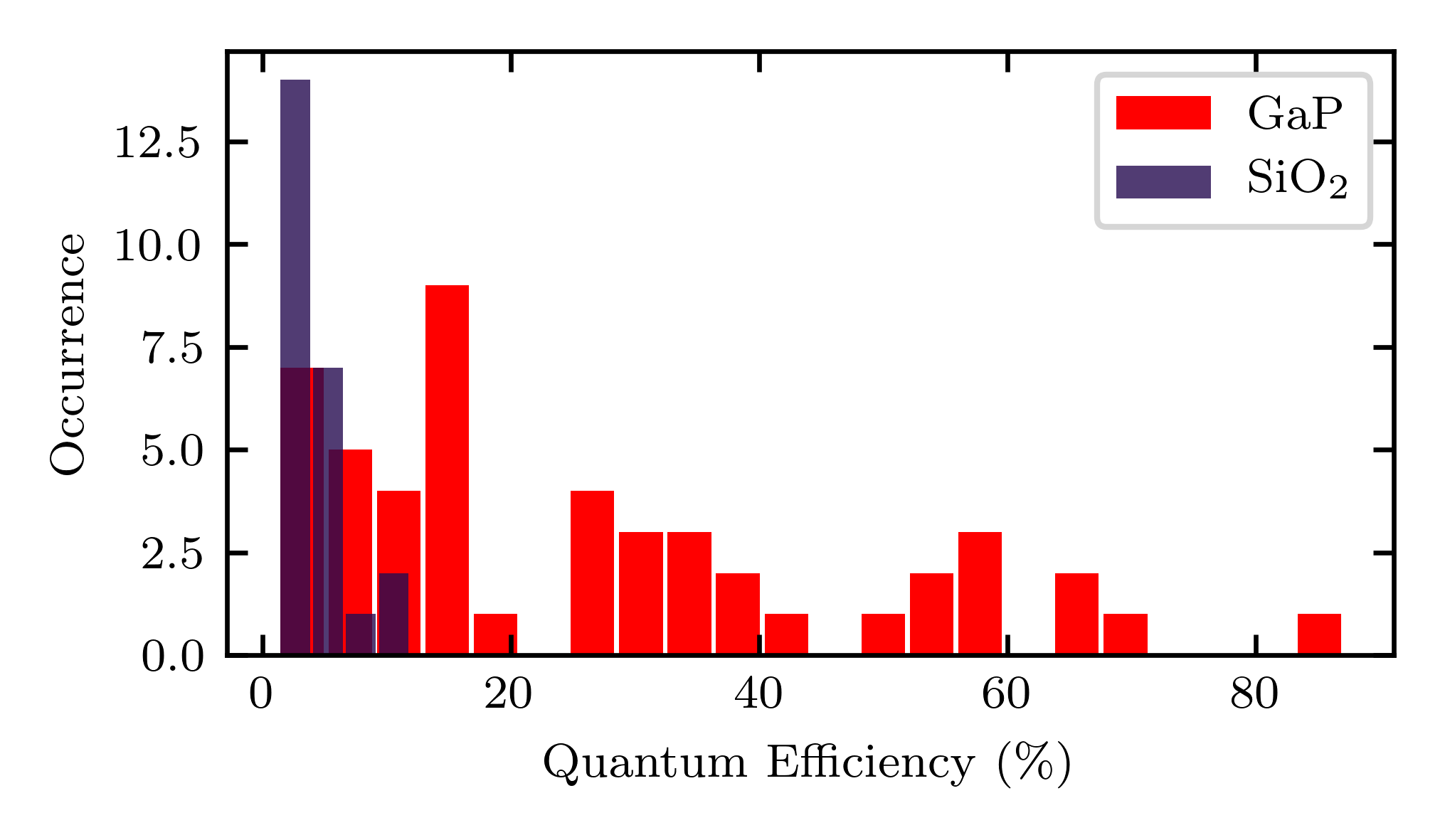
Quantum efficiency enhancement of SPEs on GaP nano-antennas. We analysed more than 50 SPEs on GaP dimer nano-antennas, with radii ranging from 150 nm up to 300 nm, selecting localized WSe2 emitters with sub-meV linewidths. For these emitters we observed common features such as linearly polarized emission, saturation of the PL intensity under increased excitation power, as well as PL lifetimes in the ns range (see Supplementary Note III). We observed no preferential orientation in the SPEs polarization, with different orientation of polarization even for emitters created on the same nano-antenna. Fig.2a shows the values of the PL intensity for SPEs on GaP nano-antennas (red dots) and on SiO2 nano-pillars (dark blue dots), acquired in the PL saturation regime and normalized to the average excitation pump power. The plot also shows the PL peak position for each studied SPE, where no correlation between the intensity and spectral position is observed. For SPEs coupled to GaP nano-antennas, we observe from two to four orders of magnitude higher power-normalized PL intensity, compared to SPEs found on SiO2 nano-pillars. Further insight into this behavior is provided by the SPE PL saturation powers, presented in Fig.2b. Since we used different repetition rates from 5 to 80 MHz in these measurements due to a large variation in the PL lifetimes, in Fig.2b we plot the energy per pulse value , defined as the time-integrated average power divided by the laser repetition rate. We readily observe more than three orders of magnitude lower saturation pulse energies for the emitters on GaP nano-antennas. In our case, 1 fJ pulse energy corresponds to the energy density per pulse of 30 nJ/cm2. Nonetheless, for such low powers, the SPEs coupled to GaP nano-antennas provide some of the highest counts per second (30,000) so far observed in TMD monolayers. In what follows, we will consider the factors that could contribute to this observation.
One of the obvious factors, expected to contribute to the reduced values of is the enhanced absorption rate () in WSe2 monolayers coupled to GaP nano-antennas. However, this can only account for a reduction of the saturation power of up to 40 times as predicted by our simulations (Fig.1d). A similar maximum enhancement for the power-normalized PL intensity may be expected due to the enhanced . Thus, additional factors need to be considered, mostly linked to the exciton dynamics and of the combined 2D-WSe2/SPE system.
In Fig.2c we compare PL lifetimes of SPEs on GaP and on SiO2. For the SPEs on the SiO2 nano-pillars we observe lifetimes of the order of 10 ns, consistent with previous reports [4, 20]. On the contrary, the SPEs on the GaP nano-antennas exhibit a broad distribution of lifetime values, ranging from 2 ns up to more than 200 ns. The radiative and non-radiative population decay rates in WSe2 SPEs ( and in Fig.3d) are dependent on the shape and confinement energy of the strain potential, and the PL decay dynamics is defined by the relationship between them: if one of the rates is much higher than the other, it will define the PL decay time.
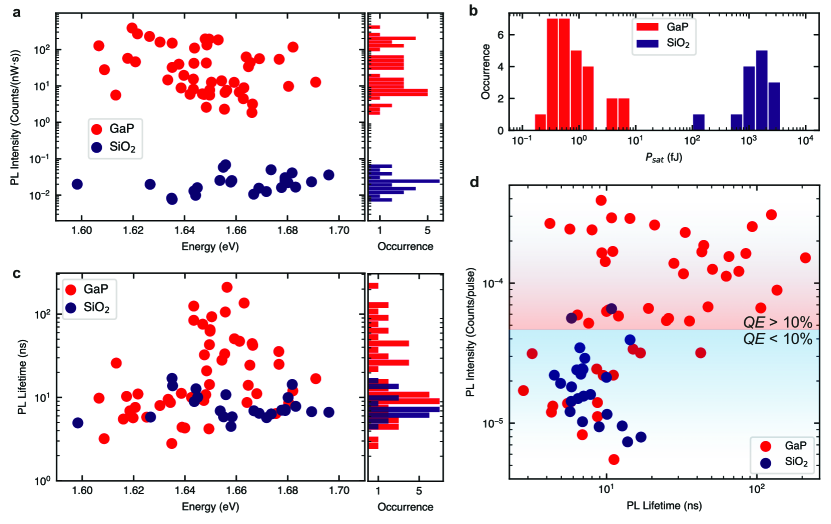
In order to shed light on the relationship between these rates, in Fig.2d we plot the SPEs fluorescence lifetime intensity distribution [32]. The SPEs on SiO2 exhibit low PL emission with relatively short lifetimes (blue area). In SPEs coupled to GaP nano-antennas we observe either a much higher PL intensity and similar lifetimes, or longer lifetimes with comparable brightness (red area in Fig.2d). The of an SPE under pulsed excitation can be estimated from the number of detected photons at saturation, divided by the laser repetition rate [8]. After taking into account the losses of the experimental set-up and the collection efficiency of the nano-antenna from numerical simulations (see additional details in Supplementary Note VI), we estimate an average for SPEs coupled to GaP nano-antennas of , with a maximum value reaching . For SPEs on SiO2 nano-pillars we estimate an average of consistent with previous reports [8].
We thus conclude that the PL decay times of SPEs on SiO2 nano-pillars are mainly defined by non-radiative processes (i.e. ), and that the true radiative lifetimes should by far exceed the measured decay times of 10 ns. On the other hand, for the SPEs on GaP nano-antennas exhibiting high , the lifetimes are mostly defined by the radiative decay (i.e. or ), which, as we can conclude from Fig.2d, vary between 2 and 200 ns. Comparing this with the SPEs on SiO2, we can conclude that the high SPEs on GaP exhibiting lifetimes of the order of 10 ns or shorter are most likely affected by the Purcell enhancement increasing their radiative rates, and thus are possibly positioned in the near-field hotspots.
The high SPEs with PL decay times 10 ns clearly must experience much slower non-radiative processes than SPEs on SiO2, as the non-radiative lifetimes must be slower than the measured PL decay times. This is also in contrast to previously reported SPEs coupled to plasmonic structures [8], where despite the very large Purcell enhancement and sub-ns PL lifetimes, the maximum of 12.6 was reported for WSe2 monolayers extracted similarly to our work from bulk crystals grown by chemical vapour transport. This implies high non-radiative rates in this system (). On the other hand, SPEs with PL lifetimes in the range of 100 ns were previously observed only in monolayer WSe2 encapsulated in hexagonal boron nitride [12], known for suppressing the non-radiative processes. In our case, possible causes for suppression of non-radiative decay could be high surface quality of crystalline GaP structures, or that some SPEs are formed in the suspended parts of the monolayer in proximity to the near-field hotspots and between the pillars [6]. We cannot exclude that some of the high SPEs with PL decay times 10 ns still experience Purcell enhancement, implying that the true radiative times in some WSe2 SPEs may reach hundreds of ns. Further detailed insight in the PL dynamics is given below in the discussion of Fig.3.
Dynamics of exciton formation in strain-induced SPEs. SPEs in WSe2 are attributed to the occurrence of strain-induced local potential minima [33, 20], essentially zero-dimensional (0D), that can host a small number of confined excitons, similar for example to semiconductor quantum dots [34]. Contrary to other group-VI TMDs, tensile strain in WSe2 results in the lowering of the conduction band (CB) minimum and the rise of the valence band (VB) maximum, as shown in Fig.3a, both located at the K points in the momentum space [35, 6]. This creates an energy landscape where a very small fraction of the 2D exciton population may be captured into such 0D centres, giving rise to non-classical light emission from confined states, at photon energies lower than that of both bright and dark excitons in unstrained WSe2.
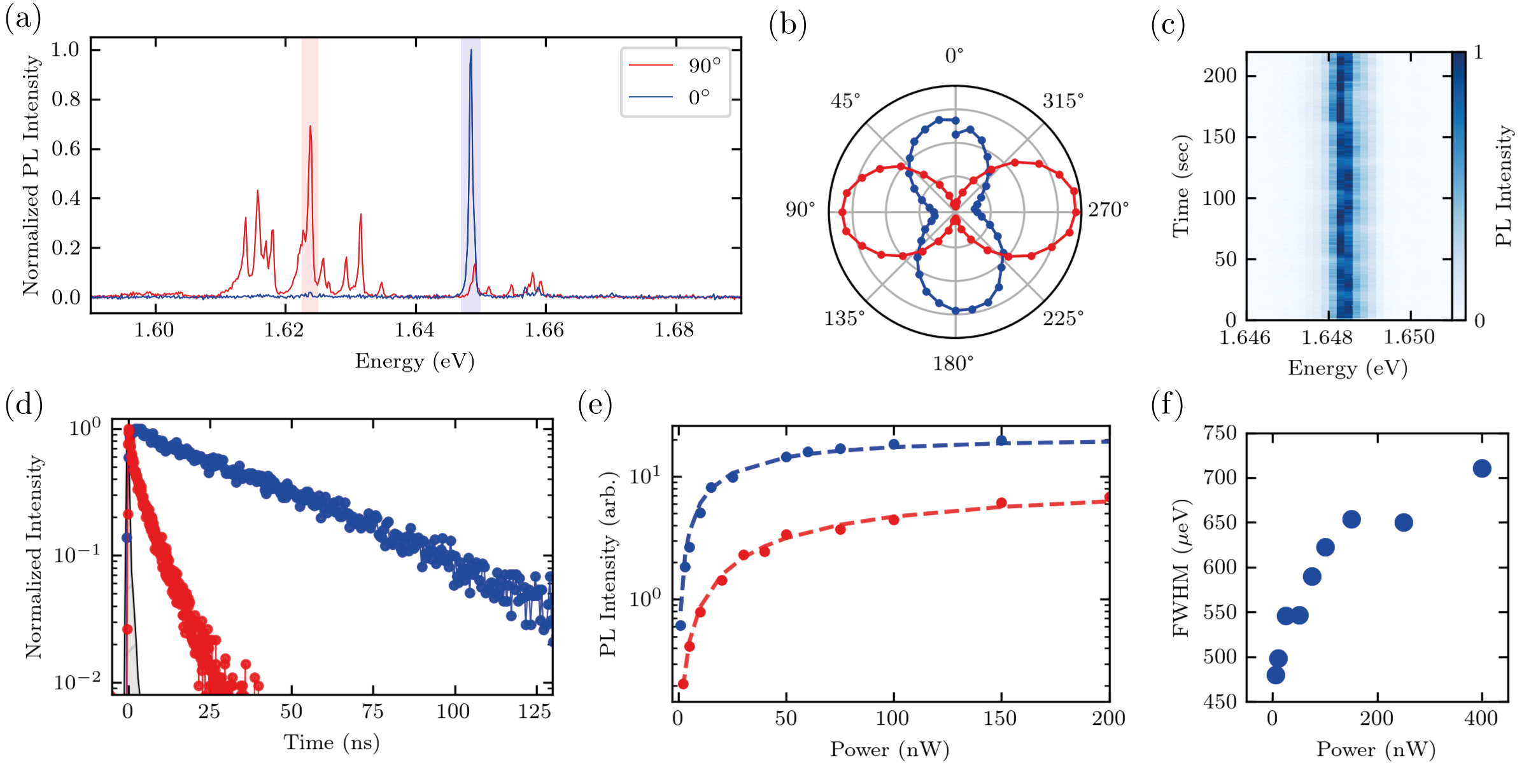
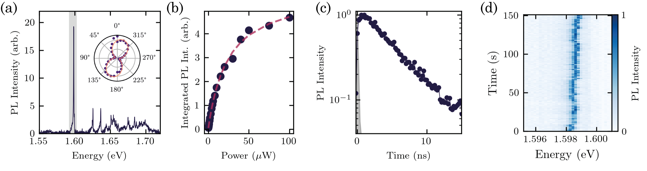
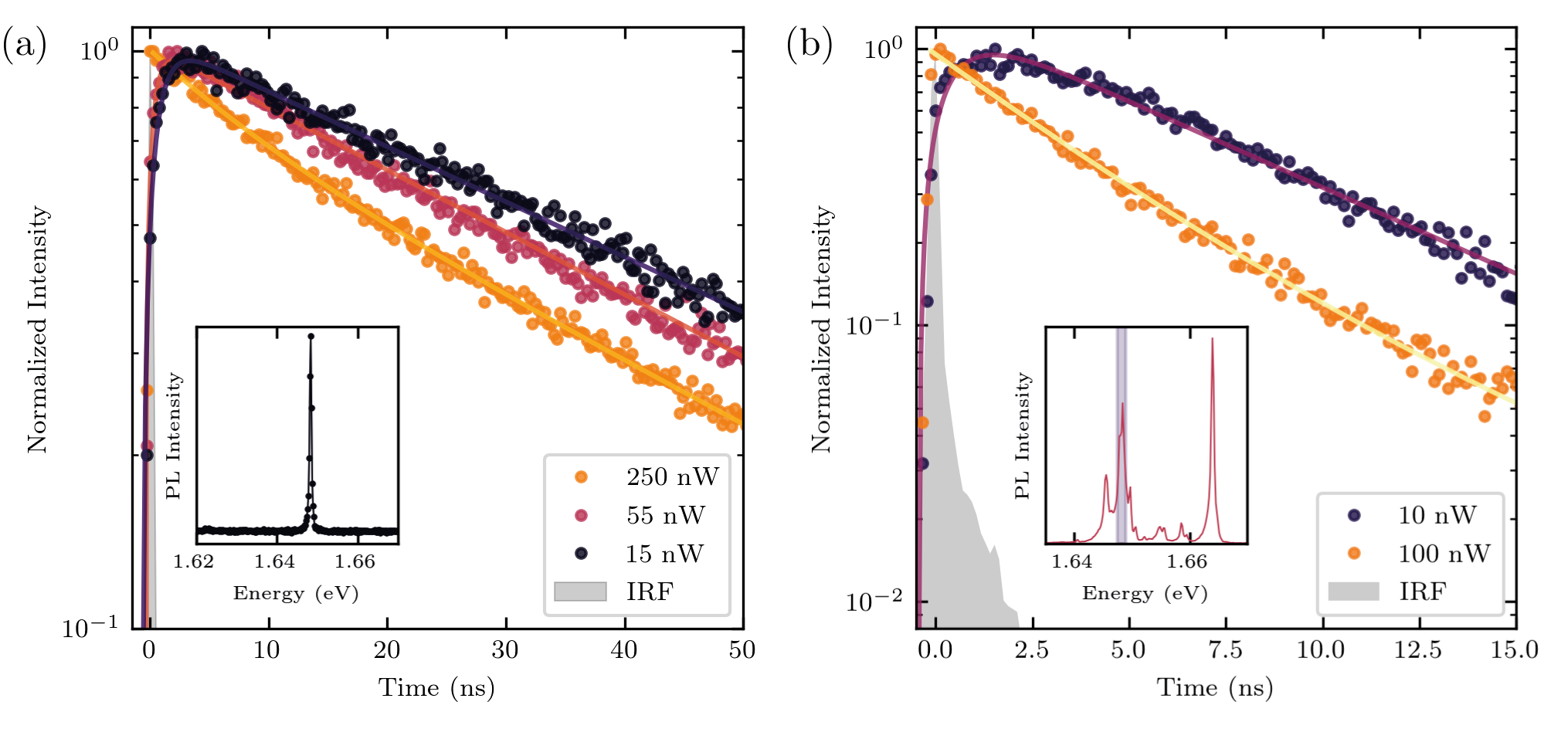
As shown in Fig.2, in the case of WSe2 placed on GaP nano-antennas, both the quantum yield and brightness of the SPEs are greatly enhanced, allowing new insight into the exciton dynamics in this hybrid 2D-0D system. Fig.3b shows a PL spectrum for an SPE exhibiting of . Fig.3c shows the time-resolved PL decay for the same SPE measured with 20 MHz repetition rate. The PL decay curves are obtained at different powers of 1, 100 and 1000 nW considerably below, close and considerably above the saturation power, respectively. For clarity, the inset zooms in on the short times after the laser pulse excitation. At low power we clearly observe a ns-scale rise time, which shortens as the power is increased also accompanied by a relatively weak shortening of the PL decay time.
We fit the data with a simple empirical model assuming an exciton reservoir, which feeds excitons into the SPE. The model can be solved analytically (see Supplementary Note VII for more details) and is used to fit the data, as shown in the inset of Fig.3c, providing rise and decay times plotted in Fig.3e-f. Here, we see that as the power is increased, the rise time, , changes strongly from 1.7 ns to times approaching the experimental resolution, whereas the PL decay time decreases from 8.5 to 7.4 ns.
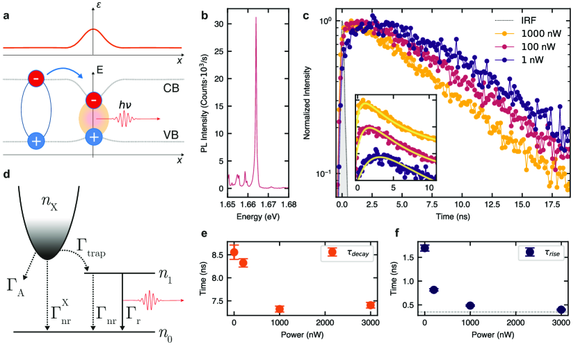
In order to understand this behavior, we consider several processes, which influence both the populations of the high energy 2D exciton reservoir and the SPE itself. We argue that the exciton reservoir with the population in Fig.3d corresponds to the population of dark excitons, which we infer from the very slow PL rise time of 1.7 ns at low power, in contrast to the expected lifetime of the bright excitons of a few ps [36, 37]. The dark excitons decay mostly via sample-specific non-radiative recombination with a rate and, importantly, via the exciton-exciton (Auger) annihilation [28, 29], which grows with the increasing power as . Trapping of dark excitons with a rate into the strain-induced SPE is responsible for a negligible reduction of , as the anti-bunching photon emission implies that only one exciton per laser excitation cycle can be created in the SPE. We thus also introduce a probability for the SPE to be filled with an exciton with . The trapping of the dark excitons is the only source of the SPE population, and is included as a term in the equations below. Here we take into account the effect of the SPE occupancy on the reduced efficiency of the exciton trapping with the factor , providing one of the mechanisms for the PL saturation with increasing power observed in the experiment. The population of the SPE decays radiatively and non-radiatively with rates and , respectively. Here, for simplicity we neglect the SPE’s internal confined state structure, which we uncover in PL excitation experiments (see Fig.4 for details). The rate equations capturing the behavior of the three-level system depicted in Fig.3d are shown below:
| (1) |
| (2) |
We estimate that for 1 nW laser power at 20 MHz repetition rate and 5 light absorption in WSe2, the dark exciton density cm-2 will be created. This is probably the lower bound, as the near-field electric field enhancement can locally lead to the increase of this value by a factor exceeding 10. At this low power limit, the Auger annihilation can be neglected [28] and the unsaturated SPE emission leads to an average (per pulse) . The PL rise dynamics is then defined by the predominately non-radiative decay of the dark exciton reservoir with the rate . As the power is increased, and both and grow, two additional processes become important: the Auger annihilation described by the term and the saturation of the SPE with the corresponding term . For the powers presented in Fig.3, is estimated to be of the order of cm-2 for the power of 100 nW and cm-2 for 1000 nW, in the range where the Auger annihilation was found to be very efficient [28, 29].
While a more detailed study at low powers could help to separate the contributions from the Auger annihilation and SPE saturation, it is possible that in the high power regime the SPE PL saturation is influenced not only by the state-filling effect, but also by the non-radiative depletion of the dark exciton reservoir. In the case of the bright and high SPEs in WSe2/GaP nano-antenna system, high photon counts can be achieved at low excitation powers, thus circumventing the requirement for increased pumping. On the other hand, in the SPEs in WSe2 on SiO2 nano-pillars, where both the and brightness are low, increased pumping is required to observe the SPE PL. This has a negative effect on the population of the reservoir via the Auger annihilation and thus, through such negative feedback, leads to the requirement to further increase the power. Eventually, both the low and its further reduction due to the Auger annihilation lead to a very large three order of magnitude increase in the saturation powers in the SPEs in WSe2 on SiO2 nano-pillars compared with those on GaP nano-antennas, as seen in Fig.2. In support of these conclusions, we also note that high saturation powers, similar to those observed by us in WSe2 SPEs on SiO2 were also reported in SPEs coupled to plasmonic structures [8], where very fast non-radiative processes in the 2D WSe2 should be expected.
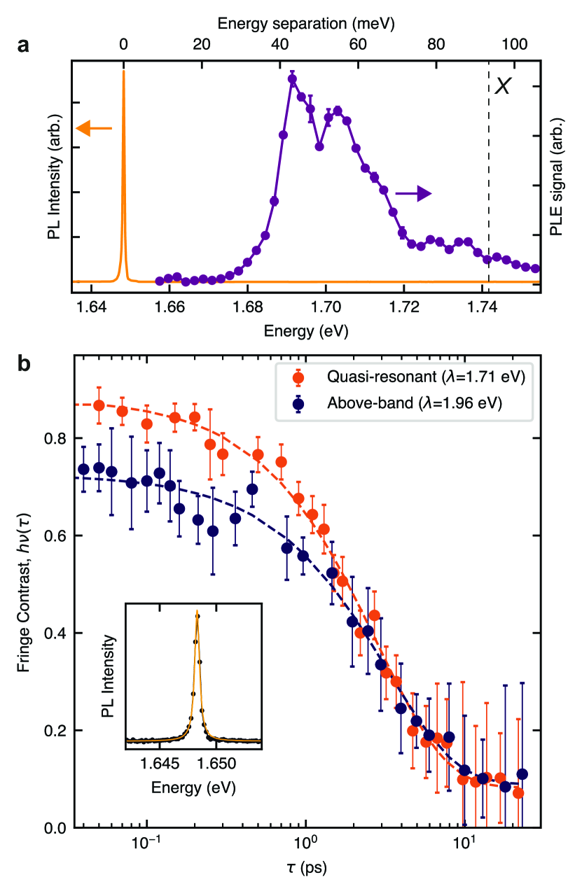
Coherence of a strain-induced SPE. The coherence of WSe2 SPEs has been previously investigated only under high power densities and non-resonant excitation [8]. Here, we evaluated the first-order correlation function, , for the SPE shown in Fig.4a, in a Mach-Zender interferometer set-up [38] and compared different excitation schemes (see Methods). We employed an above-band excitation using a 1.96 eV (638 nm) cw laser, corresponding to an energy higher than the A-exciton resonance in monolayer WSe2 (dashed line in Fig.4a). Under these conditions, high energy excitons are created in the continuum of states above the excitonic resonance, introducing dephasing for instance via scattering with phonons and impurities or via exciton-exciton interactions. To reduce the impact of such processes, we also used a quasi-resonant excitation with a cw laser at 1.71 eV (725 nm). As shown in Fig.4a, this excitation is resonant with higher energy states within the SPE [1]. Fig.4b shows the measured fringe contrast, , of the WSe2 SPE under the two excitation schemes (see Methods). By fitting the observed decay of the fringe contrast with a single exponential decay function, , we extract a coherence time of ps under quasi resonant excitation, and of ps for above band excitation. The differences between the excitation schemes have a negligible effect on the SPE dephasing time, implying a complex relaxation processes within the confined states of the SPE. We find that the PL full-width at half maximum (FWHM) of eV corresponds to ps (FWHM ) close to the observed values, indicating that the coherence of the studied SPE is limited by pure dephasing, which we attribute to interactions with phonons during the exciton relaxation [39], as for the excitation power nW used in the experiment the contribution of the Auger annihilation can be excluded. The observed SPE values are one order of magnitude higher than those reported for monolayer WSe2 of 0.3 ps [39]. Excitation in resonance with the lowest energy optical transition in the SPE could be employed to gain access to the intrinsic coherence times of the confined excitons.
Discussion
In summary, we have demonstrated that high-refractive-index GaP nano-antennas offer an efficient approach for nano-scale positioning and enhancement in strain-induced SPEs in monolayer WSe2. We found 102 to enhancement of the PL intensity for WSe2 SPEs coupled to GaP nano-antennas compared with those formed on low-refractive-index SiO2 nano-pillars. We demonstrate that this is primarily caused by the greatly increased in the 2D/0D WSe2 system coupled to GaP nano-antennas arising from the enhancement of the radiative rates in such SPEs through the Purcell effect, as well as the reduction of the non-radiative decay rates. Importantly, this allows bright emission from the SPEs to be excited with energy densities per laser pulse below 30 nJ/cm2 corresponding to the energy per pulse below 1 fJ, enabling the SPE operation at low exciton densities in the 2D WSe2, thus avoiding the exciton-exciton annihilation. The powers at which SPEs on GaP nano-antennas provide bright emission are approximately three orders of magnitude below those required for operation of the SPEs on SiO2 pillars studied in this work, as well as those previously reported for SPEs formed on plasmonic nano-structures [8], despite the large Purcell enhancement factors found in the latter system [8]. Further improvement and consistency of the operation of SPEs can possibly be achieved by employing deterministic defect placement [40, 41], while the required excitation powers can be further reduced by employing much cleaner WSe2 grown by the so-called flux technique [8]. The photon collection efficiency in our approach can be potentially improved by engineering the nanocavity geometry and materials, for instance by using nano-antennas made from high-index TMDs [42, 43]. These materials can be deposited on any type of substrate. By placing them on a metallic mirror similarly to the strategy pursued by Luo et al in Ref.[8], most of light can be redirected upwards, and the collection efficiency in the first lens can be considerably increased. Overall, our work suggests that hybrid systems composed of 2D semiconductors coupled to dielectric nano-antennas are a powerful means for controlling quantum light generation.
Methods
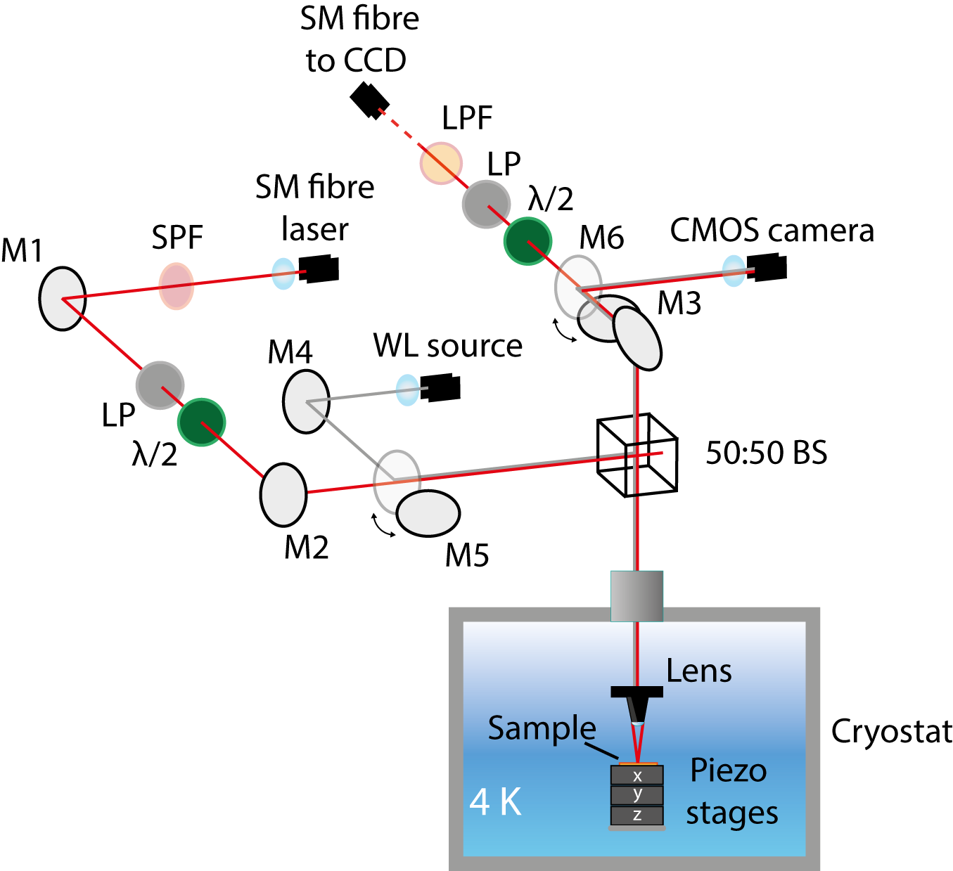
Sample fabrication The GaP dimer nano-antennas were fabricated using electron beam lithography, followed by several wet and dry etching steps as described in Ref.[24]. Arrays of nano-antennas separated by 4 m were made. The dimers had a gap of nm, a height of 200 nm and nano-pillar radii () of 150, 200, 250 and 300 nm. Atomically thin monolayers of WSe2 were mechanically exfoliated from commercially available bulk single crystals (HQ Graphene) onto polydimethylsiloxane (PDMS) polymer substrates. The monolayer thickness was identified by examining room temperature PL with an imaging method described in Ref.[44]. The monolayers were then transferred on top of the GaP nano-antenna array, by using the same PDMS substrates, with an all-dry transfer technique in a home-built transfer setup [45].
Optical spectroscopy Low temperature PL spectroscopy was carried out with a sample placed in low pressure He exchange gas within a confocal microscope platform allowing free space optical access and high precision sample positioning (Attocube). The whole microscope stick was inserted in a liquid helium transport dewar (Cryo Anlagenbau Gmbh) and a nominal sample temperature of 4 K was used in all reported experiments. The excitation from the lasers used in this work was delivered through single-mode fibres to the optical breadboard placed at the top of the microscope stick, where it was collimated and directed onto the sample through a window at the top of the stick. For pulsed excitation we used a diode laser (PicoQuant) at 638 nm, with a variable repetition rate from 5 to 80 MHz and a pulse width of 90 ps. For continuous wave excitation, we used a tunable Ti-Sapphire laser (M Squared SOLSTIS). PL emitted by the sample was collected with an aspheric lens (NA = 0.64) and coupled at the breadboard into a single-mode optical fibre, which delivered it to a spectrometer (Princeton Instruments SP2750), where it was detected with a high-sensitivity liquid nitrogen cooled charge-coupled device (Princeton Instruments PyLoN). For the time-resolved spectroscopy, the PL was also sent through the spectrometer to another exit port, where it was measured with an avalanche photodiode (ID100-MMF50) connected to a photon counting card (Becker and Hickl SP-130). A Hanbury Brown-Twiss set-up used for the evaluation of the second-order correlation function () was equipped with two superconducting nanowire single photon detectors (Single Quantum) and a similar photon counting card. The SPE was excited with a continuous wave diode laser (Thorlabs HL7302MG) at 730 nm with a power of 2 nW. Light from the SPE was directed to the nanowire detectors with a multi-mode fibre. The emitted light from the SPE was filtered with a pair of filters (Thorlabs FESH800 and Thorlabs FELH750) providing a transparency window between 750 nm and 800 nm.
Coherence measurements For evaluation of the first-order correlation function (), we used a Mach-Zender interferometer set-up [38] with a phase shifter in one arm and a variable optical delay in the other. By sweeping the voltage of the phase shifter, the interference of light emitted by the SPE was measured using an avalanche photodiode at one output port of the interferometer. By measuring the intensity at the local maxima () and minima () of the interference fringes, we evaluate the fringe contrast () as:
| (3) |
This procedure was repeated for increasing delay times, until the fringes were no longer resolved. The relationship between the fringe contrast and the first-order correlation function is given by the following equation:
| (4) |
where is the maximum resolvable fringe contrast in the set-up and is the first order correlation function excluding the fast oscillations at the emitter frequency. [38]. In the absence of any spectral diffusion, the fringe contrast as a function of time follows a single exponential decay, with an exponential fit allowing the evaluation of the coherence time () of the emitter.
Simulations The distributions of the electric field in Fig.1 were calculated with a commercial finite-difference time-domain software (Lumerical Inc.). In the simulations we illuminated the structure with a linearly polarized plane wave at 750 nm with a normal incidence from the vacuum side of the substrate. See Supplementary Note I for further details on the simulations.
Data availability
The data that support the findings of this study are available from the corresponding author upon request.
References
- Tonndorf et al. [2015] P. Tonndorf, R. Schmidt, R. Schneider, J. Kern, M. Buscema, G. a. Steele, A. Castellanos-Gomez, H. S. J. van der Zant, S. Michaelis de Vasconcellos, and R. Bratschitsch, Single-photon emission from localized excitons in an atomically thin semiconductor, Optica 2, 347 (2015).
- Srivastava et al. [2015] A. Srivastava, M. Sidler, A. V. Allain, D. S. Lembke, A. Kis, and A. Imamoğlu, Optically active quantum dots in monolayer WSe2, Nat. Nanotechnol. 10, 491 (2015).
- Koperski et al. [2015] M. Koperski, K. Nogajewski, A. Arora, V. Cherkez, P. Mallet, J.-Y. Veuillen, J. Marcus, P. Kossacki, and M. Potemski, Single photon emitters in exfoliated WSe2 structures, Nat. Nanotechnol. 10, 503 (2015).
- He et al. [2015] Y.-M. He, G. Clark, J. R. Schaibley, Y. He, M.-C. Chen, Y.-J. Wei, X. Ding, Q. Zhang, W. Yao, X. Xu, C.-Y. Lu, and J.-W. Pan, Single quantum emitters in monolayer semiconductors, Nat. Nanotechnol. 10, 497 (2015).
- Chakraborty et al. [2015] C. Chakraborty, L. Kinnischtzke, K. M. Goodfellow, R. Beams, and a. N. Vamivakas, Voltage-controlled quantum light from an atomically thin semiconductor, Nat. Nanotechnol. 10, 507 (2015).
- Wang et al. [2018] G. Wang, A. Chernikov, M. M. Glazov, T. F. Heinz, X. Marie, T. Amand, and B. Urbaszek, Colloquium : Excitons in atomically thin transition metal dichalcogenides, Rev. Mod. Phys. 90, 021001 (2018).
- Sortino et al. [2019] L. Sortino, P. G. Zotev, S. Mignuzzi, J. Cambiasso, D. Schmidt, A. Genco, M. Aßmann, M. Bayer, S. A. Maier, R. Sapienza, and A. I. Tartakovskii, Enhanced light-matter interaction in an atomically thin semiconductor coupled with dielectric nano-antennas, Nat. Commun. 10, 5119 (2019).
- Sortino et al. [2020] L. Sortino, M. Brooks, P. G. Zotev, A. Genco, J. Cambiasso, S. Mignuzzi, S. A. Maier, G. Burkard, R. Sapienza, and A. I. Tartakovskii, Dielectric Nanoantennas for Strain Engineering in Atomically Thin Two-Dimensional Semiconductors, ACS Photonics 7, 2413 (2020).
- Feierabend et al. [2019] M. Feierabend, S. Brem, and E. Malic, Optical fingerprint of bright and dark localized excitonic states in atomically thin 2D materials, Phys. Chem. Chem. Phys. 21, 26077 (2019).
- Lindlau et al. [2018] J. Lindlau, M. Selig, A. Neumann, L. Colombier, J. Förste, V. Funk, M. Förg, J. Kim, G. Berghäuser, T. Taniguchi, K. Watanabe, F. Wang, E. Malic, and A. Högele, The role of momentum-dark excitons in the elementary optical response of bilayer WSe2, Nat. Commun. 9, 2586 (2018).
- Linhart et al. [2019] L. Linhart, M. Paur, V. Smejkal, J. Burgdörfer, T. Mueller, and F. Libisch, Localized Intervalley Defect Excitons as Single-Photon Emitters in WSe2, Phys. Rev. Lett. 123, 146401 (2019).
- Dass et al. [2019] C. K. Dass, M. A. Khan, G. Clark, J. A. Simon, R. Gibson, S. Mou, X. Xu, M. N. Leuenberger, and J. R. Hendrickson, Ultra‐Long Lifetimes of Single Quantum Emitters in Monolayer WSe2/hBN Heterostructures, Adv. Quantum Technol. 2, 1900022 (2019).
- Palacios-Berraquero et al. [2016] C. Palacios-Berraquero, M. Barbone, D. M. Kara, X. Chen, I. Goykhman, D. Yoon, A. K. Ott, J. Beitner, K. Watanabe, T. Taniguchi, A. C. Ferrari, and M. Atatüre, Atomically thin quantum light-emitting diodes, Nat. Commun. 7, 12978 (2016).
- Schwarz et al. [2016] S. Schwarz, A. Kozikov, F. Withers, J. K. Maguire, A. P. Foster, S. Dufferwiel, L. Hague, M. N. Makhonin, L. R. Wilson, A. K. Geim, K. S. Novoselov, and A. I. Tartakovskii, Electrically pumped single-defect light emitters in WSe2, 2D Mater. 3, 025038 (2016).
- Clark et al. [2016] G. Clark, J. R. Schaibley, J. Ross, T. Taniguchi, K. Watanabe, J. R. Hendrickson, S. Mou, W. Yao, and X. Xu, Single Defect Light-Emitting Diode in a van der Waals Heterostructure, Nano Lett. 16, 3944 (2016).
- Blauth et al. [2018] M. Blauth, M. Jürgensen, G. Vest, O. Hartwig, M. Prechtl, J. Cerne, J. J. Finley, and M. Kaniber, Coupling Single Photons from Discrete Quantum Emitters in WSe2 to Lithographically Defined Plasmonic Slot Waveguides, Nano Lett. 18, 6812 (2018).
- Peyskens et al. [2019] F. Peyskens, C. Chakraborty, M. Muneeb, D. Van Thourhout, and D. Englund, Integration of single photon emitters in 2D layered materials with a silicon nitride photonic chip, Nat. Commun. 10, 4435 (2019).
- Flatten et al. [2018] L. C. Flatten, L. Weng, A. Branny, S. Johnson, P. R. Dolan, A. A. P. Trichet, B. D. Gerardot, and J. M. Smith, Microcavity enhanced single photon emission from two-dimensional WSe2, Appl. Phys. Lett. 112, 191105 (2018).
- Palacios-Berraquero et al. [2017] C. Palacios-Berraquero, D. M. Kara, A. R.-P. Montblanch, M. Barbone, P. Latawiec, D. Yoon, A. K. Ott, M. Loncar, A. C. Ferrari, and M. Atatüre, Large-scale quantum-emitter arrays in atomically thin semiconductors, Nat. Commun. 8, 15093 (2017).
- Branny et al. [2017] A. Branny, S. Kumar, R. Proux, and B. D. Gerardot, Deterministic strain-induced arrays of quantum emitters in a two-dimensional semiconductor, Nat. Commun. 8, 15053 (2017).
- Luo et al. [2018] Y. Luo, G. D. Shepard, J. V. Ardelean, D. A. Rhodes, B. Kim, K. Barmak, J. C. Hone, and S. Strauf, Deterministic coupling of site-controlled quantum emitters in monolayer WSe2 to plasmonic nanocavities, Nat. Nanotechnol. 13, 1137 (2018).
- Caldarola et al. [2015] M. Caldarola, P. Albella, E. Cortés, M. Rahmani, T. Roschuk, G. Grinblat, R. F. Oulton, A. V. Bragas, and S. A. Maier, Non-plasmonic nanoantennas for surface enhanced spectroscopies with ultra-low heat conversion, Nat. Commun. 6, 7915 (2015).
- Koshelev and Kivshar [2021] K. Koshelev and Y. Kivshar, Dielectric Resonant Metaphotonics, ACS Photonics 8, 102 (2021).
- Cambiasso et al. [2017] J. Cambiasso, G. Grinblat, Y. Li, A. Rakovich, E. Cortés, and S. A. Maier, Bridging the Gap between Dielectric Nanophotonics and the Visible Regime with Effectively Lossless Gallium Phosphide Antennas, Nano Lett. 17, 1219 (2017).
- Kolchin et al. [2015] P. Kolchin, N. Pholchai, M. H. Mikkelsen, J. Oh, S. Ota, M. S. Islam, X. Yin, and X. Zhang, High Purcell Factor Due To Coupling of a Single Emitter to a Dielectric Slot Waveguide, Nano Lett. 15, 464 (2015).
- Cihan et al. [2018] A. F. Cihan, A. G. Curto, S. Raza, P. G. Kik, and M. L. Brongersma, Silicon Mie resonators for highly directional light emission from monolayer MoS2, Nat. Photonics 12, 284 (2018).
- Koenderink [2017] A. F. Koenderink, Single-Photon Nanoantennas, ACS Photonics 4, 710 (2017).
- Mouri et al. [2014] S. Mouri, Y. Miyauchi, M. Toh, W. Zhao, G. Eda, and K. Matsuda, Nonlinear photoluminescence in atomically thin layered WSe2 arising from diffusion-assisted exciton-exciton annihilation, Phys. Rev. B 90, 155449 (2014).
- Danovich et al. [2016] M. Danovich, V. Zólyomi, V. I. Fal’ko, and I. L. Aleiner, Auger recombination of dark excitons in WS2 and WSe2 monolayers, 2D Mater. 3, 035011 (2016).
- Albella et al. [2013] P. Albella, M. A. Poyli, M. K. Schmidt, S. A. Maier, F. Moreno, J. J. Sáenz, and J. Aizpurua, Low-Loss Electric and Magnetic Field-Enhanced Spectroscopy with Subwavelength Silicon Dimers, J. Phys. Chem. C 117, 13573 (2013).
- Mignuzzi et al. [2019] S. Mignuzzi, S. Vezzoli, S. A. R. Horsley, W. L. Barnes, S. A. Maier, and R. Sapienza, Nanoscale Design of the Local Density of Optical States, Nano Lett. 19, 1613 (2019).
- Morozov et al. [2020] S. Morozov, E. L. Pensa, A. H. Khan, A. Polovitsyn, E. Cortés, S. A. Maier, S. Vezzoli, I. Moreels, and R. Sapienza, Electrical control of single-photon emission in highly charged individual colloidal quantum dots, Sci. Adv. 6, eabb1821 (2020).
- Liu and Hersam [2019] X. Liu and M. C. Hersam, 2D materials for quantum information science, Nat. Rev. Mater. 4, 669 (2019).
- Warburton et al. [2000] R. J. Warburton, C. Schäflein, D. Haft, F. Bickel, A. Lorke, K. Karrai, J. M. Garcia, W. Schoenfeld, and P. M. Petroff, Optical emission froma charge-tunable quantum ring, Nature 405, 926 (2000).
- Chang et al. [2013] C.-H. Chang, X. Fan, S.-H. Lin, and J.-L. Kuo, Orbital analysis of electronic structure and phonon dispersion in MoS2, MoSe2, WS2 and WSe2 monolayers under strain, Phys. Rev. B 88, 195420 (2013).
- Godde et al. [2016] T. Godde, D. Schmidt, J. Schmutzler, M. Aßmann, J. Debus, F. Withers, E. M. Alexeev, O. Del Pozo-Zamudio, O. V. Skrypka, K. S. Novoselov, M. Bayer, and A. I. Tartakovskii, Exciton and trion dynamics in atomically thin MoSe2 and WSe2 : Effect of localization, Phys. Rev. B 94, 165301 (2016).
- Fang et al. [2019] H. H. Fang, B. Han, C. Robert, M. A. Semina, D. Lagarde, E. Courtade, T. Taniguchi, K. Watanabe, T. Amand, B. Urbaszek, M. M. Glazov, and X. Marie, Control of the Exciton Radiative Lifetime in van der Waals Heterostructures, Phys. Rev. Lett. 123, 067401 (2019).
- Brash et al. [2019] A. J. Brash, J. Iles-Smith, C. L. Phillips, D. P. S. McCutcheon, J. O’Hara, E. Clarke, B. Royall, L. R. Wilson, J. Mørk, M. S. Skolnick, A. M. Fox, and A. Nazir, Light Scattering from Solid-State Quantum Emitters: Beyond the Atomic Picture, Phys. Rev. Lett. 123, 167403 (2019).
- Dey et al. [2016] P. Dey, J. Paul, Z. Wang, C. E. Stevens, C. Liu, A. H. Romero, J. Shan, D. J. Hilton, and D. Karaiskaj, Optical Coherence in Atomic-Monolayer Transition-Metal Dichalcogenides Limited by Electron-Phonon Interactions, Phys. Rev. Lett. 116, 127402 (2016).
- Klein et al. [2021] J. Klein, L. Sigl, S. Gyger, K. Barthelmi, M. Florian, S. Rey, T. Taniguchi, K. Watanabe, F. Jahnke, C. Kastl, V. Zwiller, K. D. Jöns, K. Müller, U. Wurstbauer, J. J. Finley, and A. W. Holleitner, Engineering the Luminescence and Generation of Individual Defect Emitters in Atomically Thin MoS2, ACS Photonics 8, 669 (2021).
- Parto et al. [2021] K. Parto, S. I. Azzam, K. Banerjee, and G. Moody, Defect and strain engineering of monolayer WSe2 enables site-controlled single-photon emission up to 150 K, Nat. Commun. 12, 3585 (2021).
- Zotev et al. [2021] P. G. Zotev, Y. Wang, L. Sortino, T. S. Millard, N. Mullin, D. Conteduca, M. Shagar, A. Genco, J. K. Hobbs, T. F. Krauss, and A. I. Tartakovskii, Transition metal dichalcogenide dimer nano-antennas with ultra-small gaps, Preprint at https://arxiv.org/abs/2105.09201, (2021) .
- Verre et al. [2019] R. Verre, D. G. Baranov, B. Munkhbat, J. Cuadra, M. Käll, and T. Shegai, Transition metal dichalcogenide nanodisks as high-index dielectric Mie nanoresonators, Nat. Nanotechnol. 14, 679 (2019).
- Alexeev et al. [2017] E. M. Alexeev, A. Catanzaro, O. V. Skrypka, P. K. Nayak, S. Ahn, S. Pak, J. Lee, J. I. Sohn, K. S. Novoselov, H. S. Shin, and A. I. Tartakovskii, Imaging of Interlayer Coupling in van der Waals Heterostructures Using a Bright-Field Optical Microscope, Nano Lett. 17, 5342 (2017).
- Castellanos-Gomez et al. [2014] A. Castellanos-Gomez, M. Buscema, R. Molenaar, V. Singh, L. Janssen, H. S. J. van der Zant, and G. A. Steele, Deterministic transfer of two-dimensional materials by all-dry viscoelastic stamping, 2D Mater. 1, 011002 (2014).
Acknowledgments L. S., P. G. Z. and and A. I. T. thank the financial support of the European Graphene Flagship Project under grant agreements 881603 and EPSRC grant EP/S030751/1. L. S. and A. I. T. thank the European Union’s Horizon 2020 research and innovation programme under ITN Spin-NANO Marie Sklodowska-Curie grant agreement no. 676108. P. G. Z. and A. I. T. thank the European Union’s Horizon 2020 research and innovation programme under ITN 4PHOTON Marie Sklodowska-Curie grant agreement no. 721394. J. C., S. A. M., and R. S. acknowledge funding by EPSRC (EP/P033369 and EP/M013812). C. L. P., A. J. B., A. I. T. and A. M. F. acknowledge funding by EPSRC Programme Grant EP/N031776/1. S. A. M. acknowledges the Lee-Lucas Chair in Physics, the Solar Energies go Hybrid (SolTech) programme, and the Deutsche Forschungsgemeinschaft (DFG, German Research Foundation) under Germany’s Excellence Strategy – EXC 2089/1 – 390776260.
Author contributions L. S., P. G. Z., A. I. T., S. A. M. and R. S. conceived the idea of the experiment. L. S. and P. G. Z. fabricated WSe2 layers, transferred them on GaP nano-antennas, and carried out numerical modelling. L. S., P. G. Z., C. L. P. and A. J. B. carried out optical spectroscopy measurements on WSe2. J. C. fabricated GaP nano-antennas. J. C. and R. S. designed GaP nano-antennas. L. S. and E. M. designed and analysed the rate equation model. L. S., P. G. Z., C. L. P., A. J. B. and A. I. T. analysed optical spectroscopy data. S. A. M., R. S., A. M. F. and A. I. T. managed various aspects of the project. L. S., P. G. Z. and A. I. T. wrote the manuscript with contributions from all co-authors. A. I. T. oversaw the whole project.
Competing Interests The authors declare no competing interests.
Supplementary information for: Bright single-photon emitters with enhanced quantum efficiency in a two-dimensional semiconductor coupled with dielectric nano-antennas
Supplementary note I: Numerical simulations of the Photoluminescence Enhancement Factor
The PL intensity collected from a single dipole emitter coupled to an optically driven nano-antenna is highly dependent on its relative position and orientation in respect to the scattered field, defined by the vector r, and originates from three factors [1]:
| (5) |
The relative PL enhancement factor [2] is given by the ratio between PL intensity values obtained when the dipole is placed on GaP nano-antennas and on SiO2 nano-pillars, . We carried out a set of numerical finite-difference time-domain (FDTD) simulations for an in-plane dipole emitting at = 750 nm, placed either on top of GaP dimer nano-antennas, or on SiO2 nano-pillars on a SiO2(100 nm)/Si substrate. The heights of the GaP dimers and the SiO2 pillars were set to 200 nm and 100 nm, respectively, matching the structures used in our experiments. In our simulations we find that by increasing the height of SiO2 pillars, a negligible effect on their optical properties is observed due to the lack of Mie optical resonances.
The first factor in Eq.5, , describes the increased absorption cross section, dependent on the local electric field intensity , where is the intensity of the scattered radiation and the intensity of the normally incident linearly polarized plane wave. Supplementary Fig.1 shows the maxima of the local E field at the top surface of the nano-antenna ( nm) taken along the line connecting each nano-pillar centre (see Inset). In Supplementary Fig.1b we show the maximum value of the field on GaP dimers (red) and on SiO2 nano-pillars (blue). Their ratio (yellow) defines the relative field enhancement, equal to .
The second factor is the quantum efficiency of the dipole, defined as , where is the radiative decay rate and is the non-radiative decay rate. In our simulations we used an approximation for low emitters, where the non-radiative decay , and the change in can be evaluated only from the radiative decay rate enhancement defined by the Purcell factor [2], , defined as the enhancement of the energy dissipation in the numerical simulations [3], where and ar related to the dipole on planar substrate. The dipole is placed 0.5 nm above the surface and 0.5 nm away from the nano-pillar edge, as shown in Supplementary Fig.2c. The values obtained are shown in the main text in Fig.1c, where they are normalized over the same dipole placed on the flat substrate as reference.
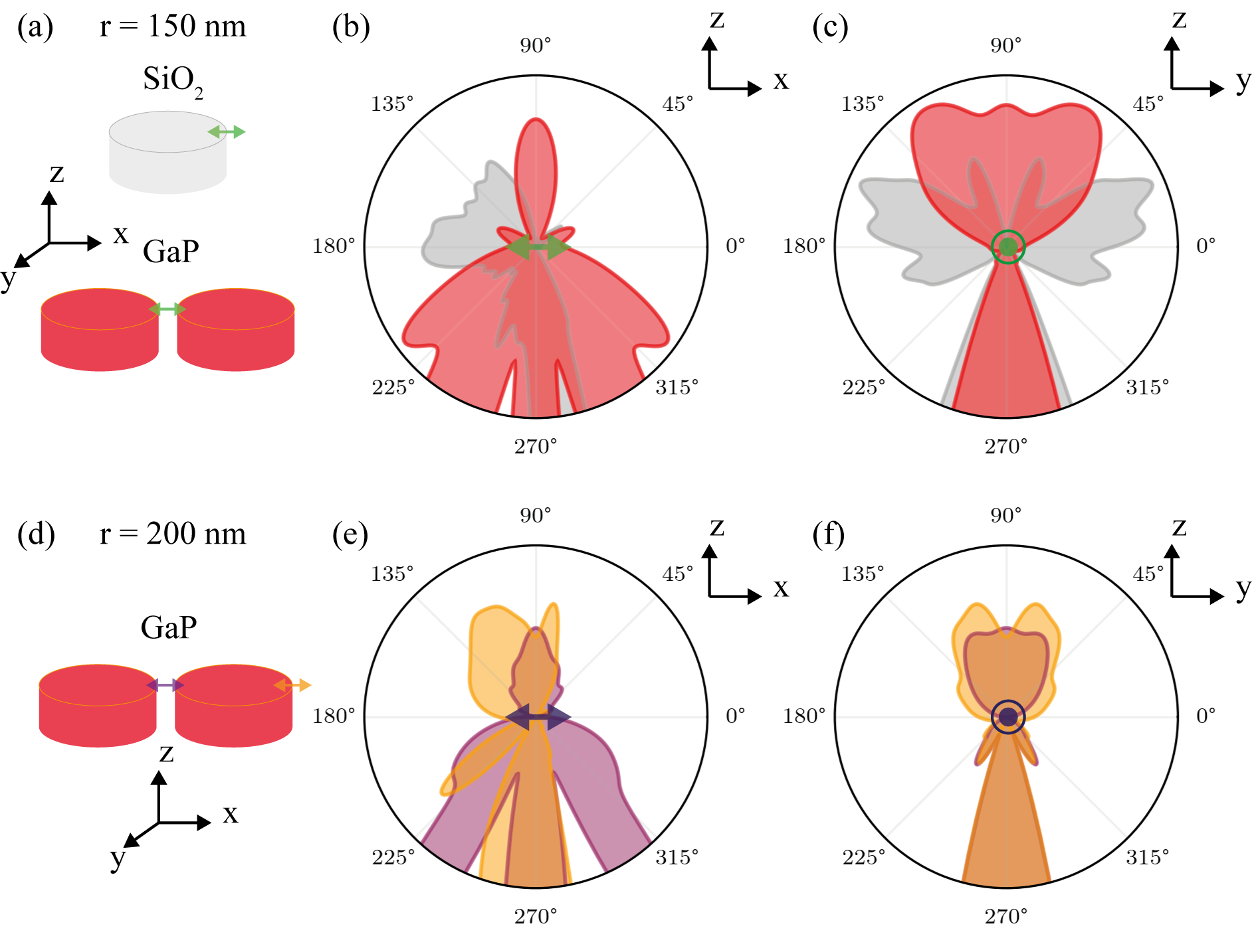
The last factor in Eq.5, , defines the fraction of the light collected by the numerical aperture () of the objective, calculated as the fraction of power emitted in the upwards direction, in a cone defined by the objective . Supplementary Fig.2a-c shows the radiation pattern for an in-plane dipole ( = 750 nm) placed at the centre of the gap of a GaP dimer nano-antenna (in red) and at the edge of a SiO2 nano-pillar (in grey). In case of GaP nano-antennas, no significant difference was observed when placing the dipole at the edge of the nano-pillar, similarly to SiO2. Due to the higher refractive index, for GaP most of the emitted light is directed downwards into the substrate. For a dipole coupled to GaP dimer nano-antennas we obtained a collection of for antennas with a radius of 300 nm, and up to for nm. For a dipole on top of a SiO2 nano-pillar, we found a collection from (r = 300 nm) up to (r = 150 nm).
In case of dimer nano-antennas larger than 150 nm we observe a larger enhancement of the collection efficiency and compared to the same dipole placed in the gap of the dimer. Following our previously published theoretical calculations [6], this is the point where tensile strain is maximised and thus where the SPEs will likely be positioned. In Supplementary Fig.2d-e we show the effect on the power radiated by a dipole placed at either the gap (purple) or at the outer edges (yellow) of a dimer nano-antenna with a radius of 200 nm.
Supplementary note II: Optical Mie resonances of GaP dimer nano-antennas
Supplementary note III: Photoluminescence and polarization properties of WSe2 single photon emitters on GaP nano-antennas
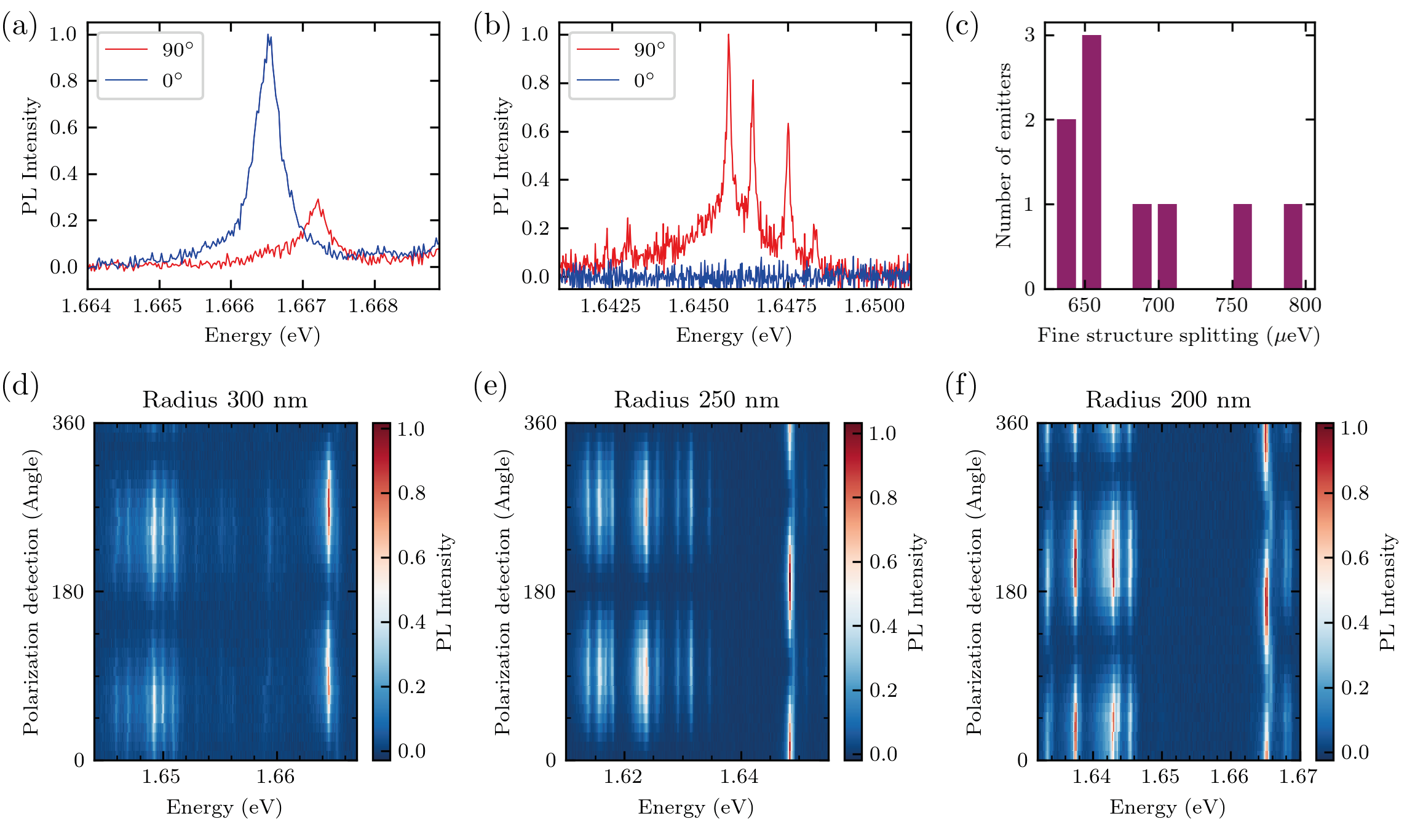
Supplementary Fig.4a shows the PL spectrum for a WSe2 monolayer on top of a GaP dimer nano-antenna ( nm) excited with a linearly polarized laser at 638 nm, and collected under two orthogonal polarization directions (blue and red traces). As shown in Supplementary Fig.4b, the single peak observed in co-polarized collection (highlighted in blue in Fig.S4a) is accompanied by a series of peaks in cross-polarized detection at lower energy (highlighted in red in Fig.S4a). The SPEs on GaP nano-antennas exhibit stable emission over time, as shown in Supplementary Fig.4c, as expected from the improved spectral wandering in highly strained monolayers [4].
As shown in Supplementary Fig.4d, we observe ns PL lifetimes, with faster dynamics for the cross-polarized peaks (red trace 7 ns) compared to the co-polarized peak (blue trace 42 ns). The emitters exhibit a similar power saturation behaviour, as shown in Supplementary Fig.4e. In Supplementary Fig.4f we show the homogeneous broadening of the linewidth (FWHM) of the SPE highlighted in blue in Fig.S4a, under increasing excitation power density, obtained by fitting the spectra with a Lorentzian peak function (see Fig.4 in the main text) . Due to the varying anisotropy of the confining potential, SPEs in WSe2 are known to exhibit emission peaks both with and without a fine structure splitting (FSS) at zero magnetic field [5]. As we show in Supplementary Fig.5a-b, we observe the presence of cross polarized peaks with FSS on the order of 600-800 eV ( Supplementary Fig.5c) and, on the same nano-antenna, peaks that show a near unity degree of linear polarization with no underlying fine structure. As shown in Supplementary Fig.5d-f, we observed a repeated pattern in the polarization from strain-induced SPEs on top of nano-antennas with different radii. The presence of a bright, high energy peak, usually exhibiting a FSS, is followed by a large number of emitters at lower energies, exhibiting the same polarization axis and no FSS. We ascribe this behaviour to different kinds of strain-induced emitters in the WSe2 layer, related to a different confinement energy and size of the potential well created by nano-scale strain inhomogeneities.
Supplementary note IV: Fabrication and photoluminescence properties of WSe2 single photon emitters on SiO2 nano-pillars
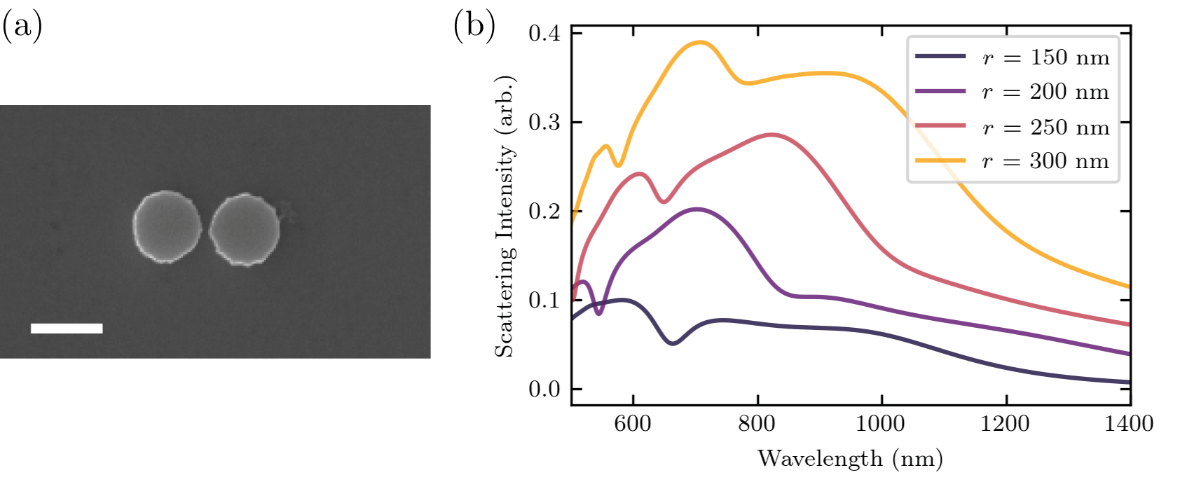
The SiO2 nano-pillars are fabricated from a thermally grown 290 nm SiO2 layer on a silicon wafer, with radii ranging from 50 to 250 nm, with an electron beam lithography and reactive ion etching system. Supplementary Fig.6a shows an electron microscope image of a resulting SiO2 nano-pillar with a radius of 200 nm and height of 100 nm. The monolayer of WSe2 is transferred onto the SiO2 nano-pillars with an all-dry transfer technique. A bright field image of the transferred monolayer is shown in Supplementary Fig.6b. Supplementary Fig.6c shows the room temperature PL map of the transferred WSe2 monolayer on top of the nano-pillar array.
Supplementary Fig.7a shows a representative cryogenic PL spectrum of a WSe2 SPE positioned on top of a SiO2 nano-pillar (highlighted in grey). The localized emitter exhibits linearly polarized emission (Inset Supplementary Fig.7a), as expected from 2D in-plane dipole emitters. The SPE further shows saturation of the PL intensity under increasing excitation power (Supplementary Fig.7b), PL decay with ns (Supplementary Fig.7c) and lower spectral stability compared to SPEs on GaP nano-antennas (Supplementary Fig.7d).
Supplementary Note V: Strain dependence of the single photon emission
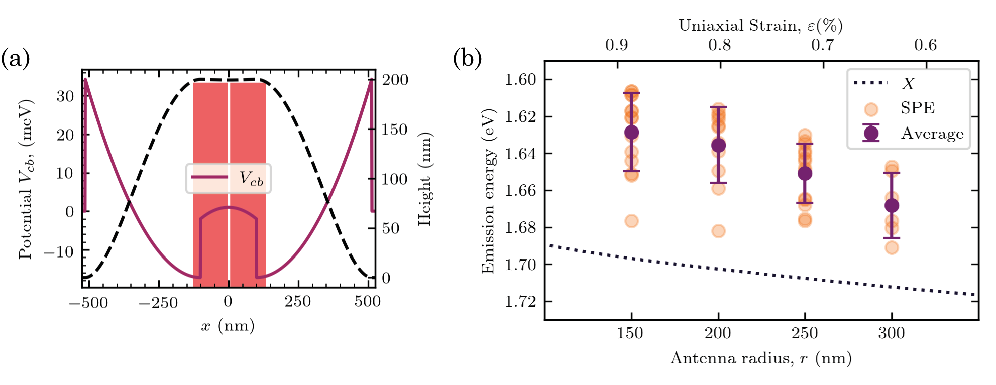
The nano-antenna geometry can be used to tailor the strain introduced in an atomically thin semiconductors as described in Ref.[6]. Supplementary Fig.8a shows the section along the x-axis, defined as in Fig.1 of the main text, of the height profile (black dashed line) of a WSe2 monolayer on top of a dimer nano-antenna (in red) and the relative change in the WSe2 conduction band potential (). The tensile strain is maximized at the edges of the nano-pillars (in red) and correspond to a lowering of , and directly a reduction of the band gap energy. This strain profile forms a deformation potential well which can trap excitons [6]. Where the 2D layer touches the substrate, strain becomes compressive and the is increased.
In Supplementary Fig.8b we show the position of different SPEs emission wavelengths (orange dots) and their average (purple), as a function of the nano-antenna radius. The increasing red-shift of the SPEs emission energy when on smaller radii nano-antennas is related to an increased tensile strain introduced in the 2D-WSe2 membrane. These results confirm the impact of strain on the emission properties of strain-induced SPEs in two-dimensional WSe2.
Supplementary note VI: Collection and quantum efficiency of the single photon emission
The underlying quantum efficiency () of a SPE under pulsed excitation can be estimated from the laser repetition rate and the number of detected photons [8]. If for each laser pulse we detect a photon, the is 100% and the rate of photons detected matches that of the excitation laser repetition rate. We calibrated the collection efficiency by measuring the losses with a 725 nm laser. The values obtained from the calibration are listed in the table below. The values for the transmission of the linear polarizer, the spectrometer and the CCD efficiency are taken from the relative datasheet. We obtain a collection efficiency of the experimental setup of 0.56.
| Component | Transmission | |||
| Optical components (Cryostat) | 50% | |||
| Linear polarizer | 78% | |||
| Single Mode fibre coupling | 2% | |||
| Spectrometer in-coupling | 90% | |||
| Spectrometer mirrors (x3) | (97%)3=91% | |||
| Grating Efficiency | 90% | |||
| CCD Quantum Efficiency | 98% | |||
| TOTAL COLLECTION EFFICIENCY | 0.56% |
From the FDTD simulations described in Supplementary Note I, we have estimated the cavity collection efficiency as the fraction of the total power radiated inside an objective with NA=0.64, the same used in our experiments. The estimated internal quantum efficiency () is calculated as:
| (6) |
where is the collected intensity from the SPE, is the collection efficiency of the experimental setup, is the collection efficiency from numerical simulations (given in Supplementary Note I), and is the laser repetition rate. In Supplementary Fig.10 we show the estimated internal quantum efficiency for WSe2 SPEs positioned on both GaP dimer nano-antennas and SiO2 nano-pillars, corrected for the total collection efficiency and for the corresponding laser repetition rate. For SiO2, we obtain an average quantum efficiency of while for SPEs on GaP an average of with some SPEs reaching values as high as , corresponding to an overall single photon emission rate of 69 MHz and, normalized to the collection efficiency, of a single photon rate of 5.5 MHz at the first lens.
Supplementary note VII: Photoluminescence dynamics of strain-induced WSe2 single photon emitters
To obtain an analytical solution of the SPEs PL dynamics with a three level system, as discussed and depicted in Fig.3d in the main text, we use a reduced version of the model which can be solved analytically, given by the following equations:
| (7) |
where and are the populations of the SPE and dark excitons, respectively. Here, is the recombination process of the SPE state giving rise to the luminescence, considering both radiative and non-radiative processes, while , composed of both trapping rate of a single exciton into the strain-induced potential and the non-radiative decay of the exciton population . We exclude from this model the quadratic Auger term and the saturation of the dot discussed in the main text. The analytical solution to the above equation system is given by:
| (8) |
where , and and are the initial conditions for each relative rate equation. The above equation is used to fit the experimental data and obtain the values of the rise time () and decay time () shown in the main text.
Supplementary Fig.11 shows additional PL decay from different SPEs, the PL spectra of which is shown in the figure inset, and fitted with the analytical solution of the model describe above. Under increasing power, the rise time reduces below the timing resolution of our experimental setup, and the PL decay becomes a single exponential profile.
References
- Koenderink [2017] A. F. Koenderink, Single-Photon Nanoantennas, ACS Photonics 4, 710 (2017).
- Sortino et al. [2019] L. Sortino, P. G. Zotev, S. Mignuzzi, J. Cambiasso, D. Schmidt, A. Genco, M. Aßmann, M. Bayer, S. A. Maier, R. Sapienza, and A. I. Tartakovskii, Enhanced light-matter interaction in an atomically thin semiconductor coupled with dielectric nano-antennas, Nat. Commun. 10, 5119 (2019).
- Novotny and Hecht [2006] L. Novotny and B. Hecht, Principles of Nano-Optics (Cambridge University Press, Cambridge, 2006).
- Palacios-Berraquero et al. [2017] C. Palacios-Berraquero, D. M. Kara, A. R.-P. Montblanch, M. Barbone, P. Latawiec, D. Yoon, A. K. Ott, M. Loncar, A. C. Ferrari, and M. Atatüre, Large-scale quantum-emitter arrays in atomically thin semiconductors, Nat. Commun. 8, 15093 (2017).
- Kumar et al. [2016] S. Kumar, M. Brotóns-Gisbert, R. Al-Khuzheyri, A. Branny, G. Ballesteros-Garcia, J. F. Sánchez-Royo, and B. D. Gerardot, Resonant laser spectroscopy of localized excitons in monolayer WSe2, Optica 3, 882 (2016).
- Sortino et al. [2020] L. Sortino, M. Brooks, P. G. Zotev, A. Genco, J. Cambiasso, S. Mignuzzi, S. A. Maier, G. Burkard, R. Sapienza, and A. I. Tartakovskii, Dielectric Nanoantennas for Strain Engineering in Atomically Thin Two-Dimensional Semiconductors, ACS Photonics 7, 2413 (2020).
- Niehues et al. [2018] I. Niehues, R. Schmidt, M. Drüppel, P. Marauhn, D. Christiansen, M. Selig, G. Berghäuser, D. Wigger, R. Schneider, L. Braasch, R. Koch, A. Castellanos-Gomez, T. Kuhn, A. Knorr, E. Malic, M. Rohlfing, S. Michaelis de Vasconcellos, and R. Bratschitsch, Strain Control of Exciton-Phonon Coupling in Atomically Thin Semiconductors, Nano Lett. 18, 1751 (2018).
- Luo et al. [2018] Y. Luo, G. D. Shepard, J. V. Ardelean, D. A. Rhodes, B. Kim, K. Barmak, J. C. Hone, and S. Strauf, Deterministic coupling of site-controlled quantum emitters in monolayer WSe2 to plasmonic nanocavities, Nat. Nanotechnol. 13, 1137 (2018).