On-chip all-silicon thermoelectric device
The low thermal conductivity of silicon nanostructures, with respect to bulk silicon, opens excellent possibilities for thermoelectric applications because it will enable the use of silicon for the high efficient direct conversion of wasted heat into electrical power. This paves the way for the application of silicon devices for energy scavenging and green energy harvesting. We present a device with a large number of nanostructures suspended on a silicon substrate. Top-down techniques for device fabrication based on advanced lithography and anisotropic etching will be discussed. FEM simulations were also carried out to analyze the temperature trend through the nanostructures.
I Introduction
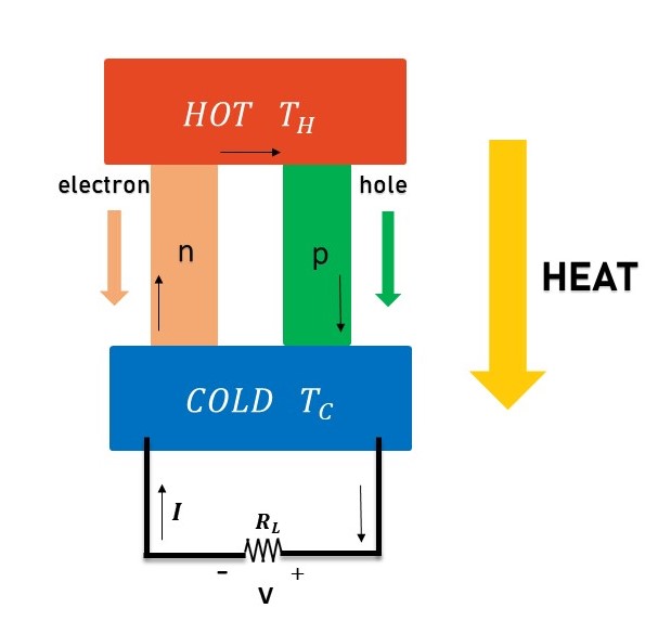
Heat is one of the most important energy sources on Earth, it represents an inexhaustible and ecological form of energy. In a global context, where the demand for electricity is always increasing, sources of sustainable energy have gained more and more interest. Given its enormous potential, there is a strong interest in researching economic technologies for the direct conversion of wasted heat into electrical energy, which so far has found application only in a few sectors for the limitations imposed by currently available thermoelectric materials. The thermoelectric effect is exploited to convert the heat provided from a source, which would otherwise be dissipated, into electricity useful for continuously powering small devices. The advantages of the thermoelectric generators (TEG) are comparable to those obtained from other renewable sources, but with the founding ideas of the circular economy: exploiting waste, or already existing sources such as the sun, wind, water or heat to obtain electricity. The purposes of TEG devices are precisely to convert heat (poor energy) into electricity (precious energy) with high efficiency. The thermoelectric conversion is based on the Seebeck effect according to which, in a circuit consisting of semiconductors, a difference of temperature generates electricity. The unit cell of a thermoelectric generatorPennelli (2014) is composed by two legs of materials with different Seebeck coefficient, placed between a hot and a cold source. These legs are electrically arranged in series and thermally in parallel. The heat flows through the two legs and determines a flow of charge carriers that generates an electrical power on the load (Figure 1).
The efficiency of TEG devices is relatedBoukay et al. (2008); Hochbaum et al. (2008) to the figure of merit, Z = : maximizing Z is equivalent to choose a material with a high electrical conductivity , a high Seebeck coefficient and a thermal conductivity as small as possible. In this context, silicon, a bio-sustainable material, abundant on Earth, offers interesting propertiesDimaggio and Pennelli (2018). Its chemical, physical and structural characteristics are well known due to its large diffusion in the nanotechnology and nano-electronics industry. However, bulk silicon, compared to other materials used for thermoelectric applications, has a high thermal conductivity, equal to 148 W/(m K). The thermal conductivity is given by the sum of two contributionsHics and Dresselhaus (1993a, b) one due to charge carriers and the other to phonons. In bulk silicon, the greatest contribution is due to the phonons, therefore the thermal conductivity can be considered approximately equal to the phonon thermal conductivity. Several works, present in the literatureLi et al. (2003, 2012); Pennelli et al. (2018a), have shown that, by reducing down to the nanoscale the dimensions of silicon structures, the thermal conductivity results in a few W/(m K)Elyamny et al. (2020). In nanostructures, the dimensions of the devices become comparable with the phonon mean free path. This leads to a reduced phonon propagation, and therefore the thermal conductivity drops to very low values. Our purpose is the development of a fabricating process for a thermoelectric device based on a large number of nanostructuresPennelli and Macucci (2016). A prototype of these thermoelectric generators was defined on top of a silicon on insulator wafer, together with an integrated metallic resistor used for the application of the three technique for the measurement of the thermal conductivity.
II Design of the device
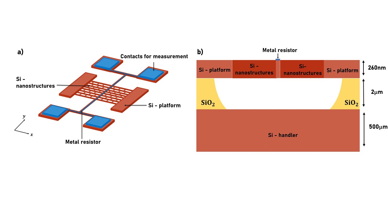
The device is based on a large array of nanostructures, fabricated on a Silicon-On-Insulator (SOI) wafer with a top silicon layer 260 nm thick, a buried oxide layer 2 m thick and an handler layer 500 m thick. The large array of nanostructures is defined on the top silicon layer by an high resolution lithographic step, followed by an anisotropic plasma etching step. The nanostructures are silicon nanoribbons, narrow down to 100nm and as tall as the thickness of the top silicon layer (260 nm). As the large side is perpendicular to the surface, this design allows the packing of a large number of nanostructures, limited by the width and the pitch between the nanoribbons. As shown in Figure 2, these nanostructures are connected to each other to increase their mechanical stability, so that they result arranged in two large grids. These two grids are suspended between two lateral large silicon platforms. The two grids are connected in the middle by a silicon ribbon, 2.4 m wide a 200 m long. In the top of the central silicon ribbon, a metal track (metal resistor) is fabricated, to be used for the thermal characterization of these grids. This central silicon ribbon is connected to top and a bottom platforms, where metal contacts for external connections are fabricated. Practically, on the central silicon ribbon a metal track (metal resistor), connecting the top and bottom metal pads, has been fabricated. The Joule heating of this metal resistor has been used for the generation of a heat flux through the suspended nnanostructures. The generated heat is then dissipated in the substrate through the two lateral silicon platforms. The main goal of this work is to characterize the heat flux through the nanostructures, in order to determine their thermal conductivity. However, the design and the main concept of this device can be easily applied to more complete on-chip devices for energy scavenging through direct thermal to electrical energy conversion.

II.1 Multiphysics simulation
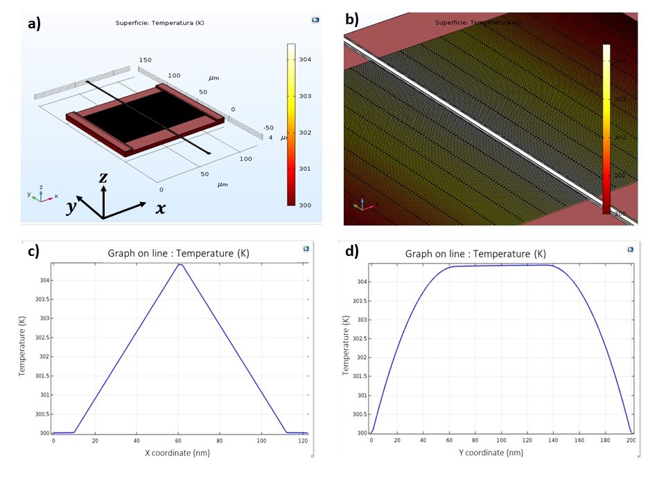
Finite Element (FEM) simulations have been performed for a correct design of the device. The software COMSOL multiphysics has been used for the simulations. As known, this software allows to solve the partial differential equations of thermal and electrical transport taking into account complex geometries, as that of the proposed devices. A suitable meshing has been performed in order to have the right rounding precision in the simulations. In order to achieve numerical values as close as possible to those of the experimental conditions, a multiphysic study has been performed: electrical transport has been considered in the metal track, where heat is generated by Joule effect; the heat transport has been simulated from the central silicon ribbon, through the suspended nanostructures, to the substrate where it is dissipated. Figure 3 shows a typical simulation. Neumann boundary conditions have been fixed for the current flux through the metal resistor; a Dirichlet boundary condition has been used to fix the temperature of the bottom of the substrate. For the silicon pads and platforms a bulk thermal conductivity of 148 W/(m K) has been considered; the thermal conductivity of the nanostructures has been fixed to 20 W/(m K), similar to that already measured on suspended silicon nanomembranes with the large side parallel to the substrateDimaggio et al. (2018). The sketch of the simulated structure is shown in panel a) of Fig. 3, and a typical result is shown in panel b) where the temperature is reported with a color scale. Panel c) shows a temperature profile along the nanostructures, taken between the suspending silicon platforms. Panel d) reports the temperature profile along the central silicon ribbon, from the top to the bottom contacts which have been fixed at 300 K. This last graph shows that the temperature is almost constant in the middle of the nanostructure grids.
III Fabrication of the device
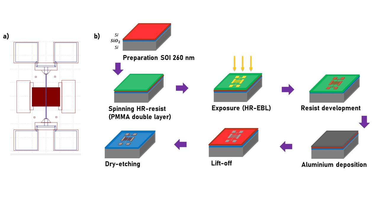
The fabrication process is based on a top-down approach on a SOI (Silicon On Insulator) wafer, following a planar strategy: the nanostructures are fabricated parallel to the surface of the silicon wafer. The process is sketched in Figure 4. At first, an aluminum mask has been defined on the top silicon layer through high resolution electron beam lithography (the design of the mask is shown in the left panel of Fig 4). To this end, standard PMMA resist has been spun on the wafer; after e-beam exposure and development, an aluminum layer 50 nm thick has been deposited by thermal evaporation, followed by lift-off in hot acetone. The shaped aluminum has been used as a mask for the highly selective plasma etching in CF4 atmosphere. Hence, the width of the nanostructures (100 nm) is defined in the lithographic step, the height is that of the top silicon layer (260 nm). After the plasma etching, the two grids of nanostructures result defined on the top silicon layer, together with the silicon platform, the silicon ribbon in the middle and the four areas on the top and on the bottom, where metal pads have been fabricated. A second lithographic step, followed by gold thermal evaporation (80 nm thick) and lift-off, has been used for the definition of the metal track (metal resistor), exactly aligned on the silicon ribbon in the middle of the grids. In the same step, metal pads, connected with the metal resistor, have been defined. The four metal pads will allow external connections for a four contact measurement of the resistance. At the end, the grids of the nanostructures have been suspended by etching the buried SiO2 layer through BHF (Buffered HF). The etching time has been calibrated for a complete removal of the oxide under the two silicon grids and the silicon ribbon in the middle, which therefore remained suspended. The silicon platforms, which are very large with respect to the grids and to the central ribbon, remained anchored to the substrate through the SiO2 layer.
Several prototypes have been fabricated, to demonstrate the feasibility of the process. Figure 5 shows some SEM images of one typical device. The images have been taken at different magnifications, to show the overall device (panel a)), the silicon grids (panel b) and c), with different magnification) and a detail of the nanostructures (panel c)). A sketch of a single nanostructure is also shown.
IV Discussion and future work
Our work demonstrates the feasibility of a process for the on-chip fabrication of large arrays of silicon nanostructures, which are interconnected and suspended on the silicon substrate. The grids are very large, if compared with the dimensions of the nanostructures, hence can drive high electrical current/high power to supply small sensor nodes. The device has been designed to allow the propagation of the heat flux from the middle of the nanostructures to the lateral supporting silicon platforms. Hence, a temperature difference can be supported, as demonstrated with numerical (FEM) simulations. Therefore, this structure is suitable for thermoelectric generator devices, which can exploit a heat source to be applied to the central ribbon. In the specific case of this work, the fabricated devices can be used for the measurement of the thermal conductivity of the grids of nanostructures. Future work will consist in applying an all-electrical technique, such as the three methodPennelli et al. (2018b), for thermal conductivity measurement: to this end, it will be exploited the Joule heating achieved by the bias of the metal resistor fabricated at the center of the grids. Moreover, the fabrication process will be improved to achieve nanostructures 100 nm wide and 1 m tall. To this end, a deep reactive plasma etching will be implemented.
References
- Pennelli (2014) G. Pennelli, Beilstein Journal of Nanotechnology 5, 1268 (2014).
- Boukay et al. (2008) A. Boukay, Y. Bunimovich, J. Tahir-Kheli, J.-K. Yu, W. A. Goddard III, and J. R. Heat, Nature Letters 451, 168 (2008).
- Hochbaum et al. (2008) A. I. Hochbaum, R. Chen, R. D. Delgrado, W. Liang, C. E. Garnett, M. Najarian, A. Majumdar, and P. Yang, Nature Letters 451, 163 (2008).
- Dimaggio and Pennelli (2018) E. Dimaggio and G. Pennelli, Nanotechnology 29, 135401 (2018).
- Hics and Dresselhaus (1993a) L. Hics and M. Dresselhaus, Physical Review B 47, 12727 (1993a).
- Hics and Dresselhaus (1993b) L. Hics and M. Dresselhaus, Physical Review B 47, 16631 (1993b).
- Li et al. (2003) D. Li, Y. Wu, P. Kim, L. Shi, P. Yang, and A. Majumdar, Appl. Phys. Lett. 83, 2934 (2003).
- Li et al. (2012) Y. Li, K. Buddharaju, B. Tinh, N. Singh, and S. J. Lee, IEEE Electron Device Letters 33, 715 (2012).
- Pennelli et al. (2018a) G. Pennelli, S. Elyamny, and E. Dimaggio, Nanotechnology 2018, 505402 (2018a).
- Elyamny et al. (2020) S. Elyamny, E. Dimaggio, S. Magagna, D. Narducci, and G. Pennelli, Nano Letters 20, 4748 (2020).
- Pennelli and Macucci (2016) G. Pennelli and M. Macucci, Semicond. Sci. Technol. 31, 054001 (2016).
- Dimaggio et al. (2018) E. Dimaggio, G. Pennelli, , and M. Macucci, IEEE Transaction on Nanotechnolgies 17, 500 (2018).
- Pennelli et al. (2018b) G. Pennelli, E. Dimaggio, and M. Macucci, Rev. of Scient. Instrum. 89, 016104 (2018b).