Double nanowires for hybrid quantum devices
Abstract
Parallel one-dimensional semiconductor channels connected by a superconducting strip constitute the core platform in several recent quantum device proposals that rely e.g. on Andreev processes or topological effects. In order to realize these proposals, the actual material systems must have high crystalline purity and the coupling between the different elements should be controllable in terms of their interfaces and geometry. We present a strategy for synthesizing double InAs nanowires by the vapor-liquid-solid mechanism using III-V molecular beam epitaxy. A superconducting layer is deposited onto nanowires without breaking vacuum, ensuring pristine interfaces between the superconductor and the two semiconductor nanowires. The method allows for a high yield of merged as well as separate parallel nanowires, with full or half-shell superconductor coatings. We demonstrate their utility in complex quantum devices by electron transport measurements.
University of Copenhagen] Center for Quantum Devices, Niels Bohr Institute, University of Copenhagen, 2100 Copenhagen, Denmark University of Copenhagen] Center for Quantum Devices, Niels Bohr Institute, University of Copenhagen, 2100 Copenhagen, Denmark University of Copenhagen] Center for Quantum Devices, Niels Bohr Institute, University of Copenhagen, 2100 Copenhagen, Denmark University of Copenhagen] Center for Quantum Devices, Niels Bohr Institute, University of Copenhagen, 2100 Copenhagen, Denmark University of Copenhagen] Center for Quantum Devices, Niels Bohr Institute, University of Copenhagen, 2100 Copenhagen, Denmark University of Copenhagen] Center for Quantum Devices, Niels Bohr Institute, University of Copenhagen, 2100 Copenhagen, Denmark University of Copenhagen] Center for Quantum Devices, Niels Bohr Institute, University of Copenhagen, 2100 Copenhagen, Denmark Budapest University of Technology and Economics] Department of Physics, Budapest University of Technology and Economics and Nanoelectronics ’Momentum’ Research Group of the Hungarian Academy of Sciences, Budafoki ut 8, 1111 Budapest, Hungary University of Copenhagen] Center for Quantum Devices, Niels Bohr Institute, University of Copenhagen, 2100 Copenhagen, Denmark University of Copenhagen] Center for Quantum Devices, Niels Bohr Institute, University of Copenhagen, 2100 Copenhagen, Denmark
1 1. Introduction
The current progress in quantum technology goes hand-in-hand with advances in materials science1. Within solid state devices, hybrid semiconductor nanowires (NWs) have attracted attention as experimental model systems for quantum computing approaches, including gate-tunable superconducting qubits2, 3, 4 and devices for studies of Majorana modes that may act as topologically protected qubits 5, 6. A number of recent proposals are based on multiple coupled nanowires, not yet realized experimentally. For example, pairs of parallel nanowires are at the core of the setup for fractional Majorana fermions that require the one-dimensionality of the individual nanowires combined with inter-wire coupling by crossed Andreev reflections 7. The resulting “parafermions” are expected to enable topological protection on a wider set of operations than Majorana mode qubits thanks to their richer topological structure. Another interesting scenario is the topological Kondo effect 8, 9 that could be realised by joining two NWs in the topological regime by a common superconducting island. Similar double nanowire geometries could lead to tuning of Majorana regimes 10, Majorana box qubits with projection control 11 and other coupled bound state systems, including Andreev bound state molecules 12, 13. These proposals all serve to show that building double nanowires (DNWs) could be key for demonstrating a suite of exotic phenomena and testing hypotheses not accessible with only individual superconducting hybrid NWs.
Harnessing the materials properties of DNWs would be essential since all the proposals require extremely well defined wire geometries and interfaces, including control of the inter-wire spacing, ranging from direct contact and tunneling between the semiconductors to purely electrostatic coupling. Most single nanowire studies have been based on bottom-up synthesized III-V semiconductor nanowires, e.g. InAs and InSb, normally grown by the vapor-liquid-solid (VLS) mechanism that yields single-crystal, one-dimensional semiconductors with diameters around 100 nm. By coating these with epitaxial superconducting shells the base materials for the single nanowire qubit schemes were formed 2, 14, 15. However, assembling such nanostructures in pairs or even more complex circuits is a challenge. The incentive to grow VLS nanowires in coupled configurations has recently led to X-junction and ”hashtag” devices 16, 17, 18 as well as demonstrations of three-dimensional branched ”tree” structures19, 20, the latter not being compatible with conventional planar device manufacture.
Until now pairs of parallel, identical nanowires coupled by a superconducting layer have not been rationally synthesized. Such hybrid double nanowires (DNWs) would directly fit in standard device fabrication schemes, see Figs. 1g-i for examples. However, so far realization of DNWs has only been possible by randomly depositing NWs on a substrate and localizing pairs that stick together21, or by identifying nanowires that accrete during VLS growth by accident. The first approach has recently been used for devices showing Cooper pair splitting in superconductor-DNW junctions 22, 23, but these techniques do not allow for the crucial controlled in-situ deposition of an epitaxial superconducting shell2, 15. Conversely, in-situ formation of hybrid DNWs would allow for the clean, uniform superconductor-semiconductor interface needed to reach the new regimes discussed above.
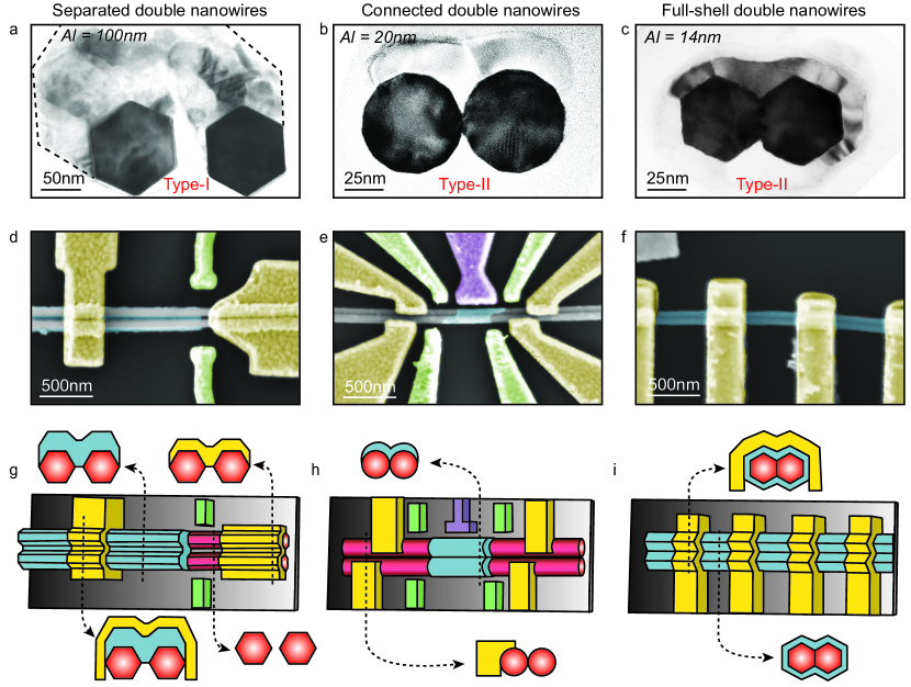
In this work we show highly reliable methods for producing DNWs based on pairs of InAs nanowires positioned next to each other during VLS growth. To grow nanowires spaced from each other in a ”train track” geometry (denoted type I), the growth parameters are set to yield rigid nanowires, ensuring that the separation between the nanowires remains constant from top to bottom. These structures are realized with a superconductor (Al) half-shell and full-shell configuration while still retaining a separation between the nanowires; see a cross section in Fig. 1a. In a different approach (denoted type II), the growth parameters are set to yield longer and comparably less rigid nanowires. Here the nanowire pairs connect in their upper segments before the metal deposition as van der Waals forces clamp the two nanowires together in an ”Eiffel tower” configuration, yielding directly connected NWs (Fig. 1b-c). The DNW geometry can be easily tuned by change of growth parameters and adjustment of the initial Au particle dimensions and inter-particle separation.
Below we describe in more detail the synthesis and design criteria behind these structures and demonstrate that they can be readily implemented in selected quantum devices (Figs. 1d-f). We note that these materials have recently been exploited for studies of Andreev molecular states 24, double quantum dot Josephson junctions 25 (Fig. 1d) and Little-Parks oscillations using full-shell DNWs 26 (Fig. 1f), demonstrating that ready-made DNWs are useful in functional quantum devices. Finally, we show designs that extend beyond the double-wire configurations and may enable experiments that can by no means be realized by serendipitous DNW formation.
2 2. Growth of parallel nanowires
Molecular beam epitaxy (MBE) is used to grow double InAs nanowires with a Wurtzite crystal structure along the [0001]B direction on InAs (111)B substrates. The double nanowires are grown via the vapor-liquid solid (VLS) mechanism and catalyzed by a pair of electron-beam lithography (EBL) defined Au particles. To facilitate growth of pairs of nanowires in very close proximity, the Au particles are engineered and patterned according to the intended inter-nanowire geometry (type I/II), while the MBE growth procedure itself is similar to one used for conventional single nanowires. To have precise control of the Au catalyst particles (disc radius ) and their separation (), multiple electron beam dot exposures (”single shots”) are positioned in a pre-defined pattern with a dot separation of 20 nm. The typical disc thickness and radius is around 20 nm and 25-50 nm, respectively (see Supplementary Information for details on Au particle formation and growth procedures). Growth of double nanowires follows largely the single nanowire growth dynamics, however, the close proximity of the nanowires reduces the contribution of adatoms to the liquid due to the shared adatom collection area on the substrate 27. In InAs nanowire growth, the main adatom contribution consists of In atoms and thus a higher effective V/III flux ratio is attained for double nanowires. With the current growth parameters this causes the double nanowires to be thinner compared to single nanowires. This effect can readily be counteracted in MBE by change of nominal fluxes. Growth parameters and a comparative analysis of single and double nanowire growth are presented in Supplementary Information, section 4. After VLS growth of the semiconductor nanowires, an aluminum layer is deposited onto nanowires by electron beam evaporation in a separate metal deposition chamber connected directly to the MBE system. The evaporation of the aluminum film follows the procedure outlined in Ref. 28 where a low substrate temperature ( K) and high rate (3 Å/s) are found to ensure a pristine bi-crystal interface while maintaining a flat and continuous morphology14, 28.
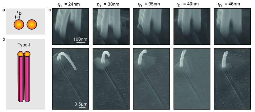
Arrays of double nanowires are defined by the lithographic patterning of Au particles prior to the growth. In order to obtain various double nanowire configurations we define fields where the separation between the centers of the Au particles is varied from, e.g., 50 nm to 300 nm at intervals of 10 nm while also varying the Au disc radius. With this strategy, we find nanowires that are too far apart and therefore stand as single nanowires as well as Au particles that are too close and combine to nucleate a single nanowire. However, importantly, we ensure the formation of extended arrays of parallel nanowires with appropriate inter-nanowire spacings, independent of fluctuations between growths and minor adjustments of growth parameters.
Figure 2 shows InAs nanowires grown with varied Au particle radii and a constant initial Au-droplet center-center separation of 160 nm. To close the gap between the nanowire pairs, a thick layer ( nm) of Al was deposited with an angle of with respect to the normal of the gap between the nanowires. The SEM micrographs in Fig. 2c are obtained at an angle opposite to the Al deposition direction in order to highlight the morphology of the nanowires. The top row focuses on the base of the nanowires, while the bottom row reveals the shading effects on the substrate. From Fig. 2, pronounced thickness-dependent bending of the nanowires is observed as seen also for single nanowires14, 29. By examining the metal deposited on the substrate, it appears that all semiconductor nanowires grow separately and in a later stage connect via the Al film, in accordance with TEM studies of cross-sections such as Fig. 1a. For the specific conditions used for the growths in Fig. 2, diameters greater than 80 nm yield a uniform nanowire separation, i.e. type I double nanowires. We also observe from Fig. 2c that longer nanowires with smaller diameters merge near the top. These flexible nanowires30 are accidentally clamped by van der Waals forces when vibrating in the growth chamber.
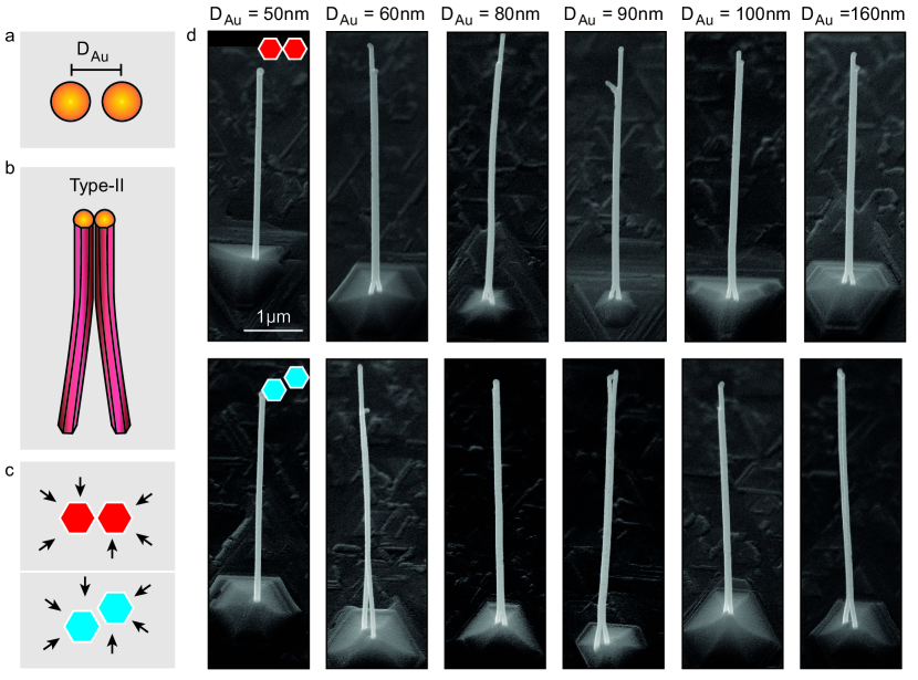
To further enhance this behaviour and thus facilitate predominantly type II merged nanowires, the growth parameters are adjusted to form thinner and longer nanowires. To decrease the average nanowire diameter for the growth shown in Fig. 3d, we increased the V/III flux ratio ( 20) by increasing the As4 flux during the axial growth step (see Supplementary Information section 4 for details). This yielded nanowires with diameters of nm for Au droplets with nm and nm for nm. To fully cover the nanowires by Al, six nm Al layers were deposited with 60∘ rotations between each evaporation, as schematically shown in Fig. 3c. Single directional evaporations are equally feasibly as shown later in Fig. 5. In Fig. 3d SEM micrographs of nanowires are shown for facet-to-facet and corner-to-corner configurations (see blue and red schematics, respectively, in Fig. 3c) with center-to-center Au particle separation varied from 50 to 160 nm and nm. The initial Au particles are positioned according to the underlying crystallographic basis of the substrate to achieve the different configurations. For all separations above 50 nm the images show consistent parallel nanowires in both configurations. A TEM micrograph of a full-shell type II cross section is shown in Fig. 1c.
Occasionally, inter-nanowire spacings and nanowire dimensions are observed to differ from the intended range, and some Au particles are found missing in post-growth SEM characterization. In rare cases the nanowires do not grow along the intended [0001]B direction. With these aberrations we find a yield of 50-60 % for type II merged nanowires as documented in Supplementary Information section 3. For these growths hundreds of identical double nanowires are found in numerous arrays across the growth substrates. We believe that most of the mishaps can be related to variations in the Au nanoparticle lithography process. The present work is not focused on optimization of the large scale yield, however, based on the demonstrated results we expect that near unity yield for double nanowire growth can be reached with optimization of the substrate preparation.
The growth dynamics for paired InAs nanowires practically follows that of conventional single nanowires, thus modifications of growth parameters can readily be used to control the crystal quality and nanowire dimensions, which is important for fulfilling the requirements in the proposed device designs. We find that it is easier to achieve a high yield of type II merged nanowires compared to type I. For the latter type, it is a challenge to define Au particles that can catalyze large (thick) nanowires whose rigidity prevents type II merging and yet are spaced close enough that the subsequent metal deposition can fill the gap between the vertical wires. One can overcome this by radially overgrowing nanowires that are nucleated by Au particles with a large height/diameter aspect ratio. Such particles show smaller displacement when they acquire the shape of a spherical cap at the growth temperatures. This approach is demonstrated in the Supplementary Information section 2.
3 3. Electrical transport characterization
We now turn to electrical transport characterization of the hybrid double nanowire system, focusing here on low temperature transport measurements of two different types of devices in the quantum regime. The objective is to demonstrate that decoupled double nanowires and multi-terminal device functionalities can be achieved (more advanced functionalities are demonstrated in forthcoming dedicated publications 24, 25, 26). Prior transport experiments on parallel nanowires have been based on individual nanowires that were accidentally merged during deposition 22, 23. In contrast, we transferred ready-made DNWs from the growth substrate to pre-patterned device substrates using a micromanipulator under an optical microscope.
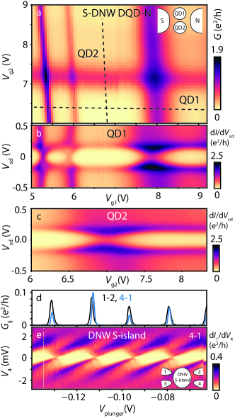
The first example is a parallel double quantum dot device formed between the superconducting in-situ deposited 100 nm Al and an ex-situ evaporated normal metal (Ti/Au) covering both wires (Fig. 1d). Prior to deposition of the normal metal, the Al on part of the nanowires has been partly removed by etching (Al etchant Transene D). The inset of Fig. 4a shows a conceptual schematic of the resulting device, where side and back gate voltage are appropriately tuned to make a superconductor (S)-parallel double quantum dot (DQD)-normal (N) device (see also Fig. 1g device schematics), however, in this case with the normal leads merged)21, 31. The conductance versus side gate voltage map plotted in Fig. 4a shows two slopes of conductance resonances (nearly horizontal/vertical), consistent with transport through two parallel quantum dots. To address the superconducting properties of the in-situ deposited Al segment, we perform bias spectroscopy along the dashed traces in Fig. 4a to independently tune the occupation of each quantum dot. For both QDs, we observe clear signs of tunneling via the superconducting coherence peaks at V shown in Fig. 4b-c in agreement with the expected superconducting energy gap of an Al film. Importantly, the two QDs appear only weakly coupled, with an upper bound given by the width of the resonances (Fig. 4a)32, in accordance with the separated ”train track” nanowire geometry (type I). Moreover, the behavior in particular for QD1 seems to reflect Yu-Shiba-Rusinov states in different coupling regimes33, 34, 35. The superconductor-DQD-normal metal device geometry is easily extended to S-parallel DQD-S Josephson junctions, where supercurrent and bound states behavior can be addressed 25, 24.
The second example is a superconducting island defined across the two nanowires, a geometry relevant for several device proposals in the topological and non-topological regimes 8, 9, 36, 37. The SEM picture in Fig. 1d shows a ”Tetris” island geometry (potentially relevant to decrease the overlap of Majorana end states on the island if it were in the topological regime), while the data discussed below were obtained on a rectangular island of length 330 nm. The superconducting island is defined by lithographic patterning and an etching step of the 17 nm thick Al film. Subsequently normal metal electrodes are defined on each nanowire following standard EBL and metal deposition recipes. The device schematics is shown in Fig. 4e, where the superconducting island — in contrast to a single nanowire device — has contact to four leads. In Fig. 4d we show the two-terminal linear conductance of two combinations of leads (1-2, 4-1) versus side gate voltage with the other terminals floating. It clearly displays Coulomb blockade behavior in the weakly coupled regime. This phenomenon is further confirmed by the bias spectroscopy measurements shown in Fig. 4e for one of the combinations revealing Coulomb blockade diamonds. The superconducting properties cannot be deduced from this data alone, but additional measurements in a different coupling regime reveal the superconducting properties in the even-odd regime via finite bias negative differential conductance features 38 facing the odd occupation of the island (to be reported in a separate work). The demonstration of Coulomb blockade via different leads to the same superconducting island is promising for investigations of the topological Kondo effect, Majorana box qubits11 and specific proposals based on the hybrid double nanowire geometry 8, 9, 36, 39, 40, 41, 42, 10, 43, 44, 37, 45, 46, 47, 48. Yet other experiments addressing the transport properties of the same double nanowire materials demonstrate coupled Andreev states24 and Yu-Shiba-Rusinov physics25 emerging in the double nanowire Josephson junction geometry. Furthermore, the full-shell double nanowire devices such as the one represented by Figs. 1c,f show Little-Parks oscillations in low-temperature transport measurements under a parallel magnetic field26, underlining that a broad range of quantum transport phenomena can be addressed in these parallel nanowire systems.
4 4. Beyond double nanowires
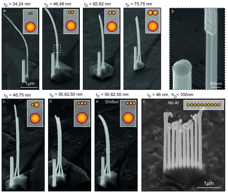
Growth substrate preparation by EBL allows the controlled fabrication of several different nanowire structures as shown in Fig. 5. Here in-situ nanowire shadowing of the subsequently deposited superconductor was furthermore implemented to allow for fabrication of hybrid devices without metal etching steps49. By fine tuning catalyst size and positioning via the EBL step it is possible to obtain a range of nanowire dimensions (Fig. 5a) and also to realize more complex heterostructures such as the shadowed triplet structure seen in Fig. 5d-e. In Fig. 5c we show that variations of the Au particle volume may be used to form nanowires with different dimensions and with that determine the overall morphology of the pairs. In turn this can be a way to provide different transport characteristics of the two nanowires, e.g. different numbers of one-dimensional subbands in DNWs with two different diameters. In Fig. 5e the triplet structure is shifted slightly to one side so that one of the three nanowires is fully coated and the remaining two are half shadowed. Finally, Fig. 5f showcases the feasibility of more complex structures, here exemplified by 10 nanowires in a row.
5 Conclusions
In conclusion, the required DNW-superconductor hybrids have been successfully developed and can be grown with a high yield. The electrical transport has elucidated the inter-wire couplings and the properties of the DNW-superconductor hybrids. Focus has so far been on realizing Al/InAs-based DNWs by MBE, but the concepts can be transferred to other III-V methods and materials that maintain an epitaxial relationship between the nanowires and the growth substrate, such as e.g. InSb and InP wires as well as other growth systems that are also utilizing the VLS mechanism for nanowire growth, e.g. metalorganic vapour phase epitaxy or chemical beam epitaxy. Likewise, the in-situ approach used here will also allow for several different metal (superconductor) coatings and other in-situ depositions, e.g. of dielectrics or magnetic materials. Finally, DNWs can also be formed from NWs with axial heterostructures.
The parallel nanowire configurations demonstrated in this work matches the requirements for several proposals within hybrid superconductor-semiconductor devices, in particular experiments within the topological regime that cannot be performed with single hybrid nanowires. Moreover, DNWs could enable experiments on Coulomb drag induced supercurrents50 in a system with low screening. Finally, bare multiwire arrangements with several parallel wires, based on structures shown in Fig. 5f, mimic the setup proposed for studying the fractional quantum Hall effect in a quantum wire array 51.
6 Author contributions
CS, KGR, JN conceived the in-situ DNW concept, TK, DO, MM, RDS, DR, JN developed growth schemes and performed structural characterizations, AV, SL, JCES, KGR, JN performed transport measurements, JN supervised the project, TK, KGR, JN wrote the manuscript with input from all authors.
This work was funded by the European Union’s Horizon 2020 research and innovation programme QuantERA project no. 127900 (SuperTOP) and FETOpen grant no. 828948 (AndQC), the Carlsberg Foundation, the Niels Bohr Institute, the Villum Foundation project no. 25310 and the Ministry of Innovation and Technology and the NKFIH within the Quantum Information National Laboratory of Hungary and by the Quantum Technology National Excellence Program (Project Nr. 2017-1.2.1-NKP-2017- 00001), NKP-20-5 New National Excellence Program. The Center for Quantum Devices is supported by the Danish National Research Foundation. J.C.E.S. acknowledges funding from the European Union’s Horizon 2020 research and innovation program under the Marie Sklodowska-Curie grant agreement No. 832645. The authors thank M. Aagesen, M. Burello, I. Nielsen, J. Paaske, G. Steffensen, M. Wauters, C.B. Sørensen, D. Laroche, D. Kjær, O. Kurtossy, Z. Scherubl, C. Schrade, J. Sestoft, and P. Makk for assistance and discussions.
References
- Giustino et al. 2021 Giustino, F.; Lee, J. H.; Trier, F.; Bibes, M.; Winter, S. M.; Valentí, R.; Son, Y.-W.; Taillefer, L.; Heil, C.; Figueroa, A. I., et al. The 2021 quantum materials roadmap. Journal of Physics: Materials 2021, 3, 042006
- Aguado 2020 Aguado, R. A perspective on semiconductor-based superconducting qubits. Appl. Phys. Lett. 2020, 117, 240501
- Larsen et al. 2015 Larsen, T. W.; Petersson, K. D.; Kuemmeth, F.; Jespersen, T. S.; Krogstrup, P.; Nygård, J.; Marcus, C. M. Semiconductor-Nanowire-Based Superconducting Qubit. Physical Review Letters 2015, 115, 127001
- Luthi et al. 2018 Luthi, F.; Stavenga, T.; Enzing, O. W.; Bruno, A.; Dickel, C.; Langford, N. K.; Rol, M. A.; Jespersen, T. S.; Nygård, J.; Krogstrup, P.; DiCarlo, L. Evolution of Nanowire Transmon Qubits and Their Coherence in a Magnetic Field. Physical Review Letters 2018, 120, 100502
- Sarma et al. 2015 Sarma, S. D.; Freedman, M.; Nayak, C. Majorana zero modes and topological quantum computation. Quantum Inf. 2015, 1, 15001
- Aasen et al. 2016 Aasen, D.; Hell, M.; Mishmash, R. V.; Higginbotham, A.; Danon, J.; Leijnse, M.; Jespersen, T. S.; Folk, J. A.; Marcus, C. M.; Flensberg, K., et al. Milestones toward Majorana-based quantum computing. Physical Review X 2016, 6, 031016
- Klinovaja and Loss 2014 Klinovaja, J.; Loss, D. Time-reversal invariant parafermions in interacting Rashba nanowires. Physical Review B 2014, 90, 045118
- Béri and Cooper 2012 Béri, B.; Cooper, N. R. Topological Kondo Effect with Majorana Fermions. Phys. Rev. Lett. 2012, 109, 156803
- Altland and Egger 2013 Altland, A.; Egger, R. Multiterminal Coulomb-Majorana Junction. Phys. Rev. Lett. 2013, 110, 196401
- Schrade et al. 2017 Schrade, C.; Thakurathi, M.; Reeg, C.; Hoffman, S.; Klinovaja, J.; Loss, D. Low-field topological threshold in Majorana double nanowires. Phys. Rev. B 2017, 96, 035306
- Plugge et al. 2017 Plugge, S.; Rasmussen, A.; Egger, R.; Flensberg, K. Majorana Box Qubits. New Journal of Physics 2017, 19, 012001
- Yang et al. 2014 Yang, Z. X.; Han, N.; Fang, M.; Lin, H.; Cheung, H. Y.; Yip, S. P.; Wang, E. J.; Hung, T. F.; Wong, C. Y.; Ho, J. C. Surfactant-assisted chemical vapour deposition of high-performance small-diameter GaSb nanowires. Nature Communications 2014, 5, 5249
- Scherübl et al. 2019 Scherübl, Z.; Pályi, A.; Csonka, S. Transport signatures of an Andreev molecule in a quantum dot–superconductor–quantum dot setup. Beilstein J. of Nanotechnology 2019, 10, 363
- Krogstrup et al. 2015 Krogstrup, P.; Ziino, N. L. B.; Chang, W.; Albrecht, S. M.; Madsen, M. H.; Johnson, E.; Nygård, J.; Marcus, C. M.; Jespersen, T. S. Epitaxy of semiconductor–superconductor nanowires. Nature Materials 2015, 14, 400–406
- Lutchyn et al. 2018 Lutchyn, R. M.; Bakkers, E.; Kouwenhoven, L. P.; Krogstrup, P.; Marcus, C.; Oreg, Y. Majorana zero modes in superconductor–semiconductor heterostructures. Nature Reviews Materials 2018, 3, 52–68
- Gazibegovic et al. 2017 Gazibegovic, S.; Car, D.; Zhang, H.; Balk, S. C.; Logan, J. A.; de Moor, M. W.; Cassidy, M. C.; Schmits, R.; Xu, D.; Wang, G., et al. Epitaxy of advanced nanowire quantum devices. Nature 2017, 548, 434–438
- Khan et al. 2020 Khan, S. A.; Lampadaris, C.; Cui, A.; Stampfer, L.; Liu, Y.; Pauka, S. J.; Cachaza, M. E.; Fiordaliso, E. M.; Kang, J.-H.; Korneychuk, S., et al. Highly Transparent Gatable Superconducting Shadow Junctions. ACS Nano 2020, 14, 14605
- Krizek et al. 2017 Krizek, F.; Kanne, T.; Razmadze, D.; Johnson, E.; Nygard, J.; Marcus, C. M.; Krogstrup, P. Growth of InAs wurtzite nanocrosses from hexagonal and cubic basis. Nano Letters 2017, 17, 6090–6096
- Dick et al. 2004 Dick, K. A.; Deppert, K.; Larsson, M. W.; Mårtensson, T.; Seifert, W.; Wallenberg, L. R.; Samuelson, L. Synthesis of branched’nanotrees’ by controlled seeding of multiple branching events. Nature materials 2004, 3, 380–384
- M. Tornberg and Lehmann 2018 M. Tornberg, K. D.; Lehmann, S. Branched InAs nanowire growth by droplet confinement. Appl. Phys. Lett. 2018, 113, 123104
- Baba et al. 2015 Baba, S.; Sailer, J.; Deacon, R. S.; Oiwa, A.; Shibata, K.; Hirakawa, K.; Tarucha, S. Superconducting transport in single and parallel double InAs quantum dot Josephson junctions with Nb-based superconducting electrodes. Applied Physics Letters 2015, 107, 222602
- Baba et al. 2018 Baba, S.; Jünger, C.; Matsuo, S.; Baumgartner, A.; Sato, Y.; Kamata, H.; Li, K.; Jeppesen, S.; Samuelson, L.; Xu, H. Q.; Schönenberger, C.; Tarucha, S. Cooper-pair splitting in two parallel InAs nanowires. New Journal of Physics 2018, 20, 063021
- Ueda et al. 2019 Ueda, K.; Matsuo, S.; Kamata, H.; Baba, S.; Sato, Y.; Takeshige, Y.; Li, K.; Jeppesen, S.; Samuelson, L.; Xu, H.; Tarucha, S. Dominant nonlocal superconducting proximity effect due to electron-electron interaction in a ballistic double nanowire. Science Advances 2019, 5, eaaw2194
- 24 Kürtössy, O.; Scherübl, Z.; Fülöp, G.; Endre Lukács, I.; Makk, P.; Kanne, J., T.and Nygård; Csonka, S. Andreev molecule in parallel InAs nanowires (preprint).
- 25 Vekris, A.; Estrada Saldaña, J. C.; Kanne, T.; Marnauza, M.; Olsteins, D.; Fan, F.; Li, X.; Hvid-Olsen, T.; Wang, X.; Qiu, X.; Xu, H. Q.; Nygård, J.; Grove-Rasmussen, K. Josephson junctions in double nanowires bridged by in-situ deposited superconductors (preprint).
- 26 Vekris, A.; Estrada Saldaña, J. C.; de Bruijckere, J.; Loric̀, S.; Kanne, T.; Marnauza, M.; Olsteins, D.; Nygård, J.; Grove-Rasmussen, K. Asymmetric Little-Parks Oscillations in Double Nanowires (preprint).
- Madsen et al. 2013 Madsen, M. H.; Krogstrup, P.; Johnson, E.; Venkatesan, S.; Mühlbauer, E.; Scheu, C.; Sørensen, C. B.; Nygård, J. Experimental determination of adatom diffusion lengths for growth of InAs nanowires. Journal of crystal growth 2013, 364, 16–22
- Kanne et al. 2020 Kanne, T.; Marnauza, M.; Olsteins, D.; Carrad, D. J.; Sestoft, J. E.; de Bruijckere, J.; Zeng, L.; Johnson, E.; Olsson, E.; Grove-Rasmussen, K.; Nygård, J. Epitaxial Pb on InAs nanowires. Nature Nanotechnology 2020,
- Bjergfelt et al. 2019 Bjergfelt, M.; Carrad, D. J.; Kanne, T.; Aagesen, M.; Fiordaliso, E. M.; Johnson, E.; Shojaei, B.; Palmstrøm, C. J.; Krogstrup, P.; Jespersen, T. S.; Nygård, J. Superconducting vanadium/indium-arsenide hybrid nanowires. Nanotechnology 2019, 30, 294005
- Erdelyi et al. 2012 Erdelyi, R.; Madsen, M.; Safran, G.; Hajnal, Z.; Lukacs, I.; Fulop, G.; Csonka, S.; Nygård, J.; Volk, J. In-situ mechanical characterization of wurtzite InAs nanowires. Solid State Communications 2012, 152, 1829
- Deacon et al. 2015 Deacon, R. S.; Oiwa, A.; Sailer, J.; Baba, S.; Kanai, Y.; Shibata, K.; Hirakawa, K.; Tarucha, S. Cooper pair splitting in parallel quantum dot Josephson junctions. Nature Communications 2015, 6, 10299
- van der Wiel et al. 2002 van der Wiel, W. G.; De Franceschi, S.; Elzerman, J. M.; Fujisawa, T.; Tarucha, S.; Kouwenhoven, L. P. Electron transport through double quantum dots. Rev. Mod. Phys. 2002, 75, 1–22
- Deacon et al. 2010 Deacon, R. S.; Tanaka, Y.; Oiwa, A.; Sakano, R.; Yoshida, K.; Shibata, K.; Hirakawa, K.; Tarucha, S. Tunneling Spectroscopy of Andreev Energy Levels in a Quantum Dot Coupled to a Superconductor. Phys. Rev. Lett. 2010, 104, 076805
- Lee et al. 2014 Lee, E. J. H.; Jiang, X.; Houzet, M.; Aguado, R.; Lieber, C. M.; de Franceschi, S. Spin-resolved Andreev levels and parity crossings in hybrid superconductor-semiconductor nanostructures. Nature Nanotechnology 2014, 9, 79–84
- Jellinggaard et al. 2016 Jellinggaard, A.; Grove-Rasmussen, K.; Madsen, M. H.; Nygård, J. Tuning Yu-Shiba-Rusinov states in a quantum dot. Phys. Rev. B 2016, 94, 064520
- Galpin et al. 2014 Galpin, M. R.; Mitchell, A. K.; Temaismithi, J.; Logan, D. E.; Béri, B.; Cooper, N. R. Conductance fingerprint of Majorana fermions in the topological Kondo effect. Phys. Rev. B 2014, 89, 045143
- Papaj et al. 2019 Papaj, M.; Zhu, Z.; Fu, L. Multichannel charge Kondo effect and non-Fermi-liquid fixed points in conventional and topological superconductor islands. Phys. Rev. B 2019, 99, 014512
- Higginbotham et al. 2015 Higginbotham, A. P.; Albrecht, S. M.; Kiršanskas, G.; Chang, W.; Kuemmeth, F.; Krogstrup, P.; Jespersen, T. S.; Nygård, J.; Flensberg, K.; Marcus, C. M. Parity lifetime of bound states in a proximitized semiconductor nanowire. Nature Physics 2015, 11, 1017–1021
- Gaidamauskas et al. 2014 Gaidamauskas, E.; Paaske, J.; Flensberg, K. Majorana Bound States in Two-Channel Time-Reversal-Symmetric Nanowire Systems. Phys. Rev. Lett. 2014, 112, 126402
- Klinovaja and Loss 2014 Klinovaja, J.; Loss, D. Time-reversal invariant parafermions in interacting Rashba nanowires. Phys. Rev. B 2014, 90, 045118
- Ebisu et al. 2016 Ebisu, H.; Lu, B.; Klinovaja, J.; Tanaka, Y. Theory of time-reversal topological superconductivity in double Rashba wires: symmetries of Cooper pairs and Andreev bound states. Progress of Theoretical and Experimental Physics 2016, 2016, 083I01
- Reeg et al. 2017 Reeg, C.; Klinovaja, J.; Loss, D. Destructive interference of direct and crossed Andreev pairing in a system of two nanowires coupled via an -wave superconductor. Phys. Rev. B 2017, 96, 081301
- Thakurathi et al. 2018 Thakurathi, M.; Simon, P.; Mandal, I.; Klinovaja, J.; Loss, D. Majorana Kramers pairs in Rashba double nanowires with interactions and disorder. Phys. Rev. B 2018, 97, 045415
- Schrade and Fu 2018 Schrade, C.; Fu, L. Parity-Controlled Josephson Effect Mediated by Majorana Kramers Pairs. Phys. Rev. Lett. 2018, 120, 267002
- Dmytruk et al. 2019 Dmytruk, O.; Thakurathi, M.; Loss, D.; Klinovaja, J. Majorana bound states in double nanowires with reduced Zeeman thresholds due to supercurrents. Phys. Rev. B 2019, 99, 245416
- Kotetes et al. 2019 Kotetes, P.; Mercaldo, M. T.; Cuoco, M. Synthetic Weyl Points and Chiral Anomaly in Majorana Devices with Nonstandard Andreev-Bound-State Spectra. Phys. Rev. Lett. 2019, 123, 126802
- Haim and Oreg 2019 Haim, A.; Oreg, Y. Time-reversal-invariant topological superconductivity in one and two dimensions. Physics Reports 2019, 825, 1–48
- Thakurathi et al. 2020 Thakurathi, M.; Chevallier, D.; Loss, D.; Klinovaja, J. Transport signatures of bulk topological phases in double Rashba nanowires probed by spin-polarized STM. Phys. Rev. Research 2020, 2, 023197
- Carrad et al. 2020 Carrad, D. J.; Bjergfelt, M.; Kanne, T.; Aagesen, M.; Krizek, F.; Fiordaliso, E. M.; Johnson, E.; Nygård, J.; Jespersen, T. S. Shadow Epitaxy for In Situ Growth of Generic Semiconductor/Superconductor Hybrids. Advanced Materials 2020, 32, 1908411
- Ji-Min Duan and Yip 1993 Ji-Min Duan, J.-M.; Yip, S. Supercurrent drag via the Coulomb interaction. Phys. Rev. Lett. 1993, 70, 3647
- Kane et al. 2002 Kane, C.; Mukhopadhyay, R.; Lubensky, T. Fractional Quantum Hall Effect in an Array of Quantum Wires. Phys. Rev. Lett. 2002, 88, 036401
Supplementary data, micrographs and discussions of parallel nanowire synthesis are found in the Supplementary Information document.