Motional narrowing, ballistic transport, and trapping of room-temperature exciton polaritons in an atomically-thin semiconductor
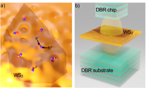
††preprint: topoAtomically-thin transition metal dichalcogenide crystals (TMDCs) hold great promise for future semiconductor optoelectronics [1] due to their unique electronic and optical properties. In particular, electron-hole pairs (excitons) in TMDCs are stable at room temperature and interact strongly with light [2]. When TMDCs are embedded in an optical microcavity, the excitons can hybridise with cavity photons to form exciton polaritons (polaritons herein) [3], which display both ultrafast velocities and strong interactions. The ability to manipulate and trap polaritons on a microchip is critical for future applications [4, 5]. Here, we create a potential landscape for room-temperature polaritons in monolayer WS2, and demonstrate their free propagation and trapping. We show that the effect of dielectric disorder, which restricts the diffusion of WS2 excitons [6] and broadens their spectral resonance [7], is dramatically reduced in the strong exciton-photon coupling regime leading to motional narrowing [8]. This enables the ballistic transport of WS2 polaritons across tens of micrometers with an extended range of partial first-order coherence. Moreover, the dephasing of trapped polaritons is dramatically suppressed compared to both WS2 excitons and free polaritons. Our results demonstrate the possibility of long-range transport and efficient trapping of TMDC polaritons in ambient conditions.
Polaritons are bosonic quasi-particles consisting of bound excitons and confined photons, which form in optical microcavities with embedded direct bandgap semiconductors [9, 10] in the strong exciton-photon coupling regime. They inherit large group velocities from their photonic component, and interact due to their excitonic component, which enables them to display collective quantum phenomena [11, 13, 14, 12] in a solid state. A roadmap of polariton-based optoelectronic devices [4] suggests multiple applications, including ultra-low threshold lasers [15] and novel computing architectures [16]. Proof-of principle demonstrations of these applications often rely on potential landscape engineering for the polaritons, e.g, by lithographic patterning, which is a well-established, advanced technology for epitaxially grown GaAs-based microcavities [5]. However, due to the low exciton binding energies in III-V semiconductor systems, their operation is limited to cryogenic temperatures. Although polariton condensation and trapping in engineered potential landscapes at room temperature were demonstrated by utilising semiconductors with large exciton binding energies [17, 18, 23, 19, 20, 21, 22], the search for the optimal polaritonic material platforms that combine stability of the samples and low disorder continues [4].
Recently, atomically-thin, two-dimensional (2D) crystals of transition metal dichalcogenides (TMDCs) have emerged as extremely promising candidates for room-temperature polaritonics due to the large exciton binding energies and strong light-matter interactions [2]. Striking properties of polaritons [3], such as the spin-valley Hall effect [24], the formation of electrically charged polaron polaritons [25], and signatures of bosonic condensation [26, 27, 28] were explored in these systems.
Here, we demonstrate room-temperature WS2 polaritons under non-resonant continuous-wave (cw) optical excitation in a high-quality all-dielectric monolithic microcavity with a non-trivial potential landscape. This potential landscape allows us to investigate both freely moving and trapped WS2 polaritons in the “thermal” regime, below the onset of bosonic condensation. Excitons in monolayer WS2 were previously shown to be profoundly affected by dielectric disorder in the environment (Fig. 1a), which causes inhomogeneous linewidth broadening [7] and reduction of the exciton diffusion coefficient due to scattering [6]. By analysing the spectrum and the first order coherence of WS2 excitons strongly coupled to the cavity photons, we find dramatic motional narrowing [8] of the inhomogeneously broadened linewidth and suppression of disorder-induced dephasing (Fig. 1b) at room temperature. Due to the drastic suppression of disorder-induced effects, WS2 polaritons exhibit strong signatures of ballistic, dissipationless propagation with conservation of total (potential and kinetic) energy and partial coherence. This enables polariton trapping in a quasi-1D potential well, even when the excitation spot is located tens of micrometers away from the trap.
The all-dielectric monolithic microcavity investigated in this work was fabricated with the flip-chip approach [24, 29], in which a small piece of a dielectric Bragg reflector (DBR) was transferred from a polypropylene carbonate (PPC) film onto a DBR substrate, at the position of a mechanically exfoliated WS2 monolayer (see Methods and Supplementary Information for details). This fabrication process fully maintains the excitonic properties of monolayer WS2 since it does not involve any direct material deposition on top of the monolayer, which can cause strong exciton quenching [30, 31].
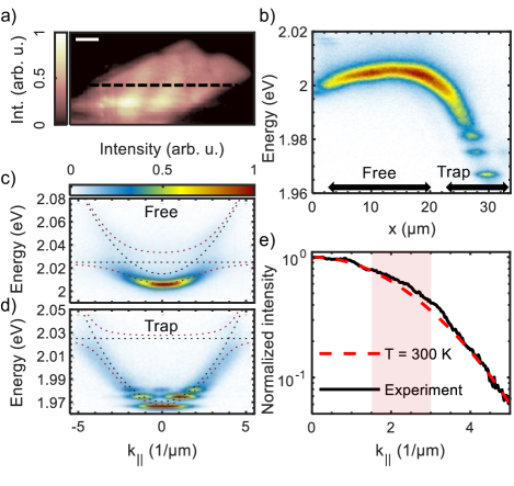
When the microcavity is excited by a continuous wave (cw) frequency doubled ND:YAG laser through a DBR Bragg minimum at , the intensity map of the photoluminescence (PL) at the position of the monolayer shows strong polariton emission (see Fig. 2a). Measuring the polariton emission spectrum along the dashed line at the angles of approximately zero incidence (see Methods) allows us to estimate the profile of the potential landscape [32] for polaritons corresponding to zero kinetic energy (). This measurement reveals the non-trivial shape (see Fig. 2b) of the potential caused by strong variation of the detuning between the cavity photon energy, , and the exciton resonance, . This variation is caused by an air gap between the DBR chip and the DBR substrate, which leads to a local modification of the cavity length.
In contrast to the approximately linear cavity wedge in GaAs-based microcavities [33], the variation of the cavity length (and ) in our system is highly nonlinear. As a result, the polariton ground state (i.e., its energy at ) considerably varies with position at and an effective trap for polaritons is formed at . The trap is a quasi-1D potential well strongly elongated in the direction perpendicular to the measurement direction, (see Supplementary Information). The angle resolved PL spectra (dispersion) in the “planar” region with a weak potential gradient () (Fig. 2c) and in the effective trap (Fig. 2d) can be well fitted with the lower (LP) and upper (UP) polariton branches , where is the exciton-photon energy detuning, and is the Rabi splitting. Therefore, the sample operates in the strong exciton-photon coupling regime at room temperature across its whole area, within a large range of detunings . The detuning defines the exciton fraction of the polariton through the excitonic Hopfield coefficient [13], which takes values and for the free and trapped polaritons, respectively (see Supplementary Information).
The occupation numbers of the momentum states of the free polaritons (at ), with the dispersion shown in Fig. 2c, are reflected in the intensity of the PL profile and can be well described with a model of a fully thermalised polariton gas [34] (see Supplementary Information) at room temperature (see Fig. 2e). In the well established model for the polariton energy relaxation under non-resonant excitation [14], polaritons reduce their kinetic energy by scattering with excitons, other polaritons and phonons. While the effective inter-particle interactions in our structure are weak due to the large binding energies and small Bohr radii of excitons [35], the observed thermalisation implies thermal equilibrium of the polariton gas with the environment and efficient polariton-phonon interactions at room temperature. The slight departure towards the higher occupation numbers in Fig. 2e occurs around the inflection point of the polariton dispersion (see Supplementary Information), referred to as relaxation bottleneck [14], where the effective mass changes sign and interaction with phonons becomes less efficient.
Quantisation of the trapped polariton spectrum is highly pronounced in Fig. 2d because the lateral size of the trap in -direction (a few micrometers) is comparable to the thermal de Broglie wavelength of polaritons [36], [37], where is the polariton effective mass extracted from the dispersion fits in Fig. 2(c,d). At K, we obtain for the free and trapped polaritons and , respectively. The ground, first, and second excited states in the trap are clearly occupied, and the energies of these states fit well to the simulation results (see Supplementary Information).
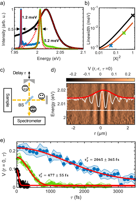
To quantify the effect of the dielectric disorder on the WS2 polaritons at room temperature, we investigate the PL of both free and trapped polaritons at by employing filtering in -space (see Methods), and compare it to the PL of bare excitons in a WS2 monolayer on the same DBR substrate. The PL spectra presented in Fig. 3a are fitted with convoluted Lorentzian and Gaussian distributions (Voigt function), corresponding to the homogeneous and inhomogeneous linewidth broadening, respectively. The homogeneous broadening is mainly determined by the radiative decay of the excitons and exciton-phonon interactions [38], and the inhomogeneous broadening is largely due to dielectric disorder on the substrate surface, which causes local fluctuations of the exciton binding energies [7]. For the excitons, we extract a total linewidth of , with the homogeneous linewidth broadening of and the inhomogeneous linewidth broadening of within % confidence level. The homogeneous linewidth broadening corresponds to , which is in good agreement with the decoherence rate of excitons in a WS2 monolayer placed on a high-quality SiO2 substrate, as determined in the four-wave mixing experiments (see Supplementary Information).
Compared to the excitons, both free and trapped polaritons display much narrower linewidths (see Fig. 3a) of and , respectively. The inhomogeneous broadening is for the free polaritons and is negligible for the trapped polaritons. Moreover, the linewidths of the free and trapped lower polaritons are substantially smaller than the theoretically calculated (see Methods) polariton linewidth (Fig. 3b, black line). The theoretical and the measured linewidths agree well only when the inhomogeneous exciton broadening is completely eliminated from the calculation (Fig. 3b, orange line). This indicates that the effects causing linewidth broadening are significantly reduced for the WS2 excitons strongly coupled to the cavity photons. This so-called motional narrowing is a well-known effect in quantum well microcavities [8, 40, 39], and was recently observed at cryogenic temperatures for excitons in monolayer MoSe2 strongly coupled to cavity photons [41] and to optical bound states in the continuum [42]. Although the exciton-photon coupling strength in our system () does not exceed the disorder-induced fluctuations of exciton binding energy (quantified by ) [40], the motional narrowing still occurs due to the size of polaritons, , significantly exceeding the spatial scale of these fluctuations [8], with the magnitude of the effect exceeding that observed in quantum well microcavities by an order of magnitude.
In addition to the linewidth broadening, dielectric disorder causes rapid dephasing of WS2 excitons (see Supplementary Information). To compare the timescales of dephasing between the excitons and polaritons, we perform the coherence measurements with a modified Michelson interferometer (see Fig. 3c) [11]. In this configuration, overlapping the original image with its flipped and time-delayed copy causes interference fringes with the visibility (see Methods):
| (1) |
where is the distance from the axis of the retro-reflector, the time delay between the interferometer arms, and is the total intensity at and (see Methods). The envelope of is a measure for the absolute value of the first order coherence function , and quantifies dephasing between and . For the coherence measurement, we remove the -space filtering to avoid filter artefacts and employ a spectrometer to be able to compare the dephasing times of the excitons, free polaritons and trapped polariton in their lowest energy states. The normalised, spectrally resolved interference pattern of the free polaritons at zero-delay is shown in Fig. 3d, together with and its envelope as a measure for . The full-width at half maximum is much larger than the theoretically expected value [37] for the thermal polariton gas . This indicates that, as a result of diminished effects of dielectric disorder, the polaritons expand without scattering-induced dephasing.
The time coherence measurements are performed at . Figure 3e shows the envelopes of for the excitons, free polaritons, and trapped polaritons around their lowest energies, fitted with a second order exponential decay function [43]. We define the time at which drops to as the decay time of the visibility . While the absolute values of extracted from the data in Fig. 3e are most likely larger than the actual dephasing times due to the spatial resolution of our experimental setup [37], their relative values scale with the relative linewidths of the excitons, free polaritons, and trapped polaritons as: , and , showing that the changes in linewidths directly correlate with the changes in dephasing times. Hence, due to the motional narrowing the dephasing of WS2 polaritons is not affected by scattering on dielectric disorder and is exclusively determined by their intrinsic decoherence and lifetimes.
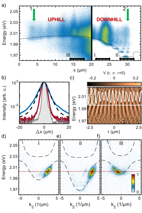
Scattering of bare WS2 excitons on disorder also causes energy dissipation and strong reduction of the diffusion coefficient [6]. In order to contrast the propagation of the WS2 polaritons with excitons, we collect the PL at the positions next to the excitation spot (see Methods). Figure 4a shows the real-space resolved PL spectra along the dashed line in Fig. 2a, when exciting the sample either at (position 1) and collecting the PL at positions (downhill), or at (position 2) and collecting the PL at positions (uphill). Strikingly, regardless of the excitation position, the polaritons travel across the whole monolayer area, both up and down the potential gradient shown in Fig. 2b, which illustrates the long-range propagation of the WS2 polaritons exceeding the mean exciton diffusion length of WS2 excitons (360 nm [44]) by orders of magnitude.
By measuring the real-space PL profile when exciting either the microcavity or the bare monolayer WS2 with a focused laser spot (positioned at for the microcavity sample), we can quantitatively compare the WS2 polariton transport with the diffusion of WS2 exciton. Figure 4b shows the emission profiles of the microcavity polaritons, the monolayer excitons, and the laser spot on logarithmic scales. It is clear that the line shape of the polariton PL strongly differs from the approximately Gaussian line profile of the laser and the monolayer PL. This is caused by the Boltzmann distribution of the thermalised polariton gas [34], in which the upper polariton branch and the lower polariton branch at higher values are well occupied at room temperature (see Fig. 2e). The corresponding modelled PL profile of the polariton gas at expanding with the maximum group velocity (black dashed line in Fig. 4b) qualitatively reproduces the measured profile, and calculations for different temperatures show that the rapid expansion of the polariton gas from the pump spot is promoted by its high temperature (see Supplementary Information). The extend of the measured profile is larger than the calculated profile most likely due to the higher polariton occupation numbers in the bottleneck region compared to the fully thermalised polariton gas (see Fig. 2b). While the exciton PL intensity drops to % at , the polariton intensity reaches this level at . For comparison, the laser excitation drops to this intensity level at , and with a (sub)linear relationship between excitation intensity and PL intensity [45] the transport length of the polaritons in this structure is at least times larger compared to the excitons.
The spatial coherence of the travelling polaritons was investigated by exciting the structure on position I in Fig. 4a and measuring the interferogram of the travelling wave packet at position II (see Fig. 4c), i.e., in the trap region. The interference fringes, extracted by removing the Doppler effect, have a substantial spatial extent, and their visibility is similar to the maximum visibility of the interference pattern at the excitation spot (see Fig. 3d). The extent of the spatial coherence can be well explained by the high kinetic energy of the travelling wave packet, and the conservation of the magnitude of the fringe visibility is a direct result of low dephasing. This finding further confirms that scattering with the disorder in the dielectric environment, which causes dephasing, is heavily reduced in the strongly light-matter coupled system.
Finally, we analyse the dispersion of the propagating polaritons by collecting the angle-resolved PL spectra from small areas in the real space (see Methods). In contrast to real-space resolved spectral imaging (Fig. 4a), in which the emitted PL is collected in all directions of the light cone, angle-resolved spectral imaging collects the PL signal limited to angles of incidences along the spectrometer slit direction. This allows us to characterise the energy spectrum of the polaritons in one particular direction , i.e. along the dashed line in Fig. 2a. First, we measure PL at positions I and II in Fig 4a, when exciting the sample at (position III). The spectra (Fig. 4d,e) unveil that the polaritons are travelling at a constant energy centred at (red dashed line in Fig. 4d,e) along the potential gradient, and that their potential energy (with respect to the global minimum) is almost fully converted into kinetic energy (i.e., the energy at measured with respect to the energy at ). The constant energy of the propagating polaritons approximately coincides with the inflection point of the polariton dispersion, i.e. the maximum value of its group velocity (see Supplementary Information). This apparent lack of the energy relaxation along the gradient is due to the low effective inter-particle interactions [35], and suppression of disorder-induced scattering, which results in the reduced energy dissipation in the system. Hence, room-temperature polaritons in WS2 can propagate ballistically over at least tens of micrometers.
Remarkably, when swapping the excitation and detection positions, i.e. exciting the polaritons at the position of the trap (position 2 in Fig. 4a), and measuring the angle-resolved PL spectra at position III in Fig. 4a, we find that the energy of the polaritons moving up the potential hill is approximately the same as the energy of the downhill flow, see Fig. 4f. This effect is also detectable in the upper polariton branch, as discussed in Supplementary Information. This uphill flow is due to the high-momenta thermalised polaritons excited in the trap region (Figure 2d) with the above-barrier kinetic energies. Without energy dissipation, these polaritons efficiently convert their high kinetic energy into potential energy while flowing uphill and populate the planar region of the sample, as observed in Fig. 4a.
Despite the constant energy flow along the gradient (-direction), clear energy relaxation and the resulting occupation of the low-energy trapped states is visible in the position-resolved spectral image (Fig. 4a, region II), which collects polariton emission from all directions, including that orthogonal to the quasi-1D trap. Weak signatures of this relaxation are visible in Fig. 4e, but the signal is stronger for the emission not filtered along . This indicates that the phonon-induced energy relaxation for room temperature polaritons is sufficient to drive the occupation of the lower energy states in the trap. The trap is occupied by polaritons even with the excitation spot located tens of micrometers away at the opposite side of the monolayer, i.e. at position (1) in Fig. 4a.
In summary, we have realised freely moving and trapped WS2 polaritons in a non-trivial potential landscape at room temperature. The pronounced motional narrowing and suppressed dephasing of the polaritons point to dramatic reduction of the effects of dielectric disorder, which strongly affect the bare exciton dynamics in monolayer TMDCs. The low dephasing and weak effective inter-particle interaction enable the polaritons to travel across tens of micrometers with minimal energy dissipation, maintaining their partial coherence. These findings offer new insights into the dynamics of WS2 polaritons at room temperature and the role of dielectric disorder in the TMDC systems strongly coupled to light. The demonstrated long-range ballistic flow and trapping of polaritons in the lowest energy states of a quasi-1D potential represent a significant step towards developing methods for manipulating and trapping polariton flow in TMDC-based polaritonic devices.
Methods
Sample Fabrication. A DBR chip splintered off a DBR substrate was placed on top of a polypropylene-carbonate (PPC) film [29], which was initially spin-coated on top of a PDMS stamp supported by a glass slide. The two halfs of the SiO2 -spacer were deposited by RF magnetron sputtering on top of the DBR chip and a DBR substrate, respectively, to ensure that the photonic field has its maximum at the centre of the microcavity. Further, a mechanically exfoliated monolayer WS2 was transferred on top of the DBR substrate. Finally, the cavity was mechanically assembled at 130 ∘C with a van der Waals stacking stage, at a temperatures at which the DBR chip detaches from the PPC film.
Experimental Setup. The photoluminescence spectra were measured with an in-house built optical setup, equipped with an array of lenses allowing for real-space (RS) and momentum-space (KS) imaging. The filtering in RS and KS were achieved with an edge-filter and an iris in the respective image planes. RS and KS imaging can be switched by flipping the lens, which images KS, in or out of the beam-path. The RS and KS spectra were measured with a spectrometer equipped with a CCD-camera and different spectrometers gratings, with 150 l/mm, 600 l/mm, and 1200 l/mm, allowing for energy resolutions down to . For the coherence measurements, we implemented a modified Michelson interferometer, where one arm is equipped with a retroreflector [11] that flips the image vertically. The output of the interferometer is fed onto the spectrometer and the interfering images are recorded using a CCD camera. The retroreflector arm is translated using a motorised stage to change the delay between the two arms.
Polariton Linewidth. To estimate the polariton linewidth, we calculate the theoretical coherence times in an ideal system for the excitons and for the microcavity photons based on their Gaussian and Lorentzian linewidth contributions [43]:
| (2) |
Here . In the strong coupling regime, the polariton coherence time is determined by the exciton and cavity photon coherence times weighted by the excitonic Hopfield coefficient [13]:
| (3) |
By using the formulas above, we deduct the theoretical values for inhomogenous and homogenous broadening from the theoretical coherence times and obtain for the total linewidth of the resulting Voigt line profiles:
| (4) |
Without inhomogeneous broadening, the polariton linewidth can be directly calculated as:
| (5) |
where is the cavity photon linewidth for the microcavity with the quality factor (see Supplementary Information).
Interference Visibility.
The interference image measured by our camera can be written as [46]:
where and correspond to the fringe frequency and relative phase, respectively. The normalised interferograms presented in this work are calculated using the formula:
The first order coherence function is the envelope of the normalised interferogram, as given by:
References
- [1] Q. H. Wang, K. Kalantar-Zadeh, A. Kis, J. N. Coleman, M. S. Strano, Electronics and optoelectronics of two-dimensional transition metal dichalcogenides, Nat. Nanotech. 7, 699-712 (2012).
- [2] C. Schneider, M. M. Glazov, T. Korn, S. Höfling, and B. Urbaszek, Two-dimensional semiconductors in the regime of strong light-matter coupling, Nat. Commun. 9, 2695 (2018).
- [3] X. Liu, T. Galfsky, Z. Sun, F. Xia, E. Lin, Y.-H. Lee, S. Kèna-Cohen, and V. M. Menon, Strong light-matter coupling in two-dimensional atomic crystals, Nat. Photon. 9, 30–34 (2015).
- [4] D. Sanvitto and S. Kèna-Cohen, The road towards polaritonic devices, Nat. Mater. 15, 1061–1073 (2016).
- [5] C. Schneider, K. Winkler, M. D. Fraser, M. Kamp, Y. Yamamoto, E. A. Ostrovskaya, and S. Höfling, Exciton-polariton trapping and potential landscape engineering, Rep. Prog. Phys. 80, 1 (2016).
- [6] J. Zipfel, M. Kulig, R. Perea-Causín, S. Brem, J. D. Ziegler, R. Rosati, T. Taniguchi, K. Watanabe, M. M. Glazov, E. Malic, and A. Chernikov, Exciton diffusion in monolayer semiconductors with suppressed disorder, Phys. Rev. B 101, 115430 (2020).
- [7] A. Raja, L. Waldecker, J. Zipfel, Y. Cho, S. Brem, J. D. Ziegler, M. Kulig, T. Taniguchi, K. Watanabe, E. Malic, T. F. Heinz, T. C. Berkelbach, and Alexey Chernikov, Dielectric disorder in two-dimensional materials, Nat. Nanotech. 14, 832–837 (2019).
- [8] D. M. Whittaker, P. Kinsley, T. A. Fisher, M .S. Skolnick, A. Armitage, A. M. Afshar, M. D. Sturge, and J. S. Roberts, Motional Narrowing in Semiconductor Microcavities, Phs. Rev. Lett. 77, 23 (1996).
- [9] A. V. Kavokin, J. J. Baumberg, G. Malpuech, F. P. Laussy, Microcavities, Oxford University Press (2017).
- [10] C. Weisbuch, M. Nishioka, A. Ishikawa, and Y. Arakawa, Observation of the coupled exciton-photon mode splitting in a semiconductor quantum microcavity, Phys. Rev. Lett. 69, 3314-3317 (1992).
- [11] J. Kasprzak, M. Richard, S. Kundermann, A. Baas, P. Jeambrun, J. M. J. Keeling, F. M. Marchetti, M. H. Szymańska, R. André, J. L. Staehli, V. Savona, P. B. Littlewood, B. Deveaud, and Le Si Dang, Bose-Einstein condensation of exciton polaritons, Nature 443, 409-414 (2006).
- [12] A. Amo, J. Lefrère, S. Pigeon, C. Adrados, C. Ciuti, I. Carusotto, R. Houdrè, E. Giacobino, and A. Bramati, Superfluidity of polaritons in semiconductor microcavities, Nat. Phys. 5, 805-810 (2009).
- [13] H. Deng, H. Haug, and Y. Yamamoto, Exciton-polariton Bose-Einstein condensation, Rev. Mod. Phys. 82, 1489 (2010).
- [14] T. Byrnes, N. Y. Kim, and Y. Yamamoto, Exciton-polariton condensates, Nat. Phys. 10, 803-813 (2014).
- [15] C. Schneider, A. Rahimi-Iman, N. Y. Kim, J. Fischer, I. G. Savenko, M. Amthor, M. Lermer, A. Wolf, L. Worschech, V. D. Kulakovskii, I. A. Shelykh, M. Kamp, S. Reitzenstein, A. Forchel, Y. Yamamoto, and S. Höfling, An electrically pumped polariton laser, Nature 497, 348-352 (2013).
- [16] D. Ballarini, M. De Giorgi, E. Cancellieri, R. Houdré, E. Giacobino, R. Cingolani, A. Bramati, G. Gigli, and D. Sanvitto, All-optical polariton transistor, Nat. Commun. 4, 1778 (2013).
- [17] J. D. Plumhof, T. Stöferle, L. Mai, U. Scherf, and R. F. Mahrt, Room-temperature Bose-Einstein condensation of cavity exciton-polaritons in a polymer, Nat. Mater. 13, 247-252 (2014).
- [18] K. S. Daskalakis, S. A. Maier, R. Murray, and S. Kéna-Cohen, Nonlinear interactions in an organic polariton condensate, Nat. Mater. 13, 271-278 (2014).
- [19] G. Lerario, A. Fieramosca, F. Barachati, D. Ballarini, K. S. Daskalakis, L. Dominici, M. D. Giorgi, S. A. Maier, G. Gigli, S. Kéna-Cohen, and D. Sanvitto, Room-temperature superfluidity in a polariton condensate, Nat. Phys. 13, 837-841 (2017).
- [20] R. Su, J. Wang, J. Zhao, J. Xing, W. Zhao, C. Diederichs, T. C. H. Liew, and Q. Xiong, Room temperature long-range coherent exciton polariton condensate flow in lead halide perovskites, Science Adv. 4, 10 (2018).
- [21] R. Su, S. Ghosh, J. Wang, S. Liu, C. Diederichs, T. C. H. Liew, and Q. Xiong, Observation of exciton polariton condensation in a perovskite lattice at room temperature, Nat. Phys. 16, 301-306 (2020).
- [22] M. Dusel, S. Betzold, O. A. Egorov, S. Klembt, J. Ohmer, U. Fischer, S. Höfling ,and C. Schneider, Room temperature organic exciton-polariton condensate in a lattice, Nat. Commun. 11, 2863 (2020).
- [23] J. Wang, W. Xie, L. Zhang, D. Xu, W. Liu, J. Lu, Y. Wang, J. Gu, Y. Chen, X. Shen, and Z. Chen, Exciton-polariton condensate induced by evaporative cooling in a three-dimensionally confined microcavity Phys. Rev. B 91, 165423 (2015).
- [24] N. Lundt, Ł. Dusanowski, E. Sedov, P. Stepanov, M. M. Glazov, S. Klembt, M. Klaas, J. Beierlein, Y. Qin, S. Tongay, M. Richard, A. V. Kavokin, S. Höfling, and C. Schneider, Optical valley Hall effect for highly valley-coherent exciton-polaritons in an atomically thin semiconductor, Nat. Nanotech. 14, 770-775 (2019).
- [25] M. Sidler, P. Back, O. Cotlet, A. Srivastava, T. Fink, M. Kroner, E. Demler, and A. Imamoglu, Fermi polaron-polaritons in charge-tunable atomically thin semiconductors, Nat. Phys. 13, 255-261 (2017).
- [26] M. Waldherr, N. Lundt, M. Klaas, S. Betzold, M. Wurdack, V. Baumann, E. Estrecho, A. Nalitov, E. Cherotchenko, H. Cai, E. A. Ostrovskaya, A. V. Kavokin, S. Tongay, S. Klembt, S. Höfling, and C. Schneider, Observation of bosonic condensation in a hybrid monolayer MoSe2-GaAs microcavity, Nat. Commun. 9, 3286 (2018).
- [27] C. Anton-Solanas, M. Waldherr, M. Klaas, H. Suchomel, H. Cai, E. Sedov, A. V. Kavokin, S. Tongay, K. Watanabe, T. Taniguchi, S. Höfling, and C. Schneider, Bosonic condensation of exciton-polaritons in an atomically thin crystal, arXiv:2009.11885 (2020).
- [28] J. Zhao, R. Su, A. Fieramosca, W. Zhao, W. Du, X. Liu, C. Diederichs, D. Sanvitto, T. C. H. Liew, and Q. Xiong, Ultralow Threshold Polariton Condensate in a Monolayer Semiconductor Microcavity at Room Temperature arXiv:2010.04381 (2020).
- [29] C. Rupprecht, N. Lundt, M. Wurdack, P. Stepanov, E. Estrecho, M. Richard, E. A. Ostrovskaya, S. Höfling, and C. Schneider, Micro-mechanical assembly and characterization of high-quality Fabry-Pèrot microcavities for the integration of two-dimensional materials, Appl. Phys. Lett. 118, 103103 (2021).
- [30] S. Y. Kim, H. I. Yang, and W. Choi, Photoluminescence quenching in monolayer transition metal dichalcogenides by Al2O3 encapsulation, App. Phys. Lett. 113, 133104 (2018).
- [31] M. Wurdack, T. Yun, E. Estrecho, N. Syed, S. Bhattacharyya, M. Pieczarka, A. Zavabeti, S.-Y. Chen, B. Haas, J. Müller, M. N. Lockrey, Q. Bao, C. Schneider, Y. Lu, M. S. Fuhrer, A. G. Truscott, T. Daeneke, and E. A. Ostrovskaya, Ultrathin Ga2O3 Glass: A Large‐Scale Passivation and Protection Material for Monolayer WS2, Adv. Mater. 3, 2005732 (2021).
- [32] M. Pieczarka, M. Boozarjmehr, E. Estrecho, Y. Yoon, M. Steger, K. West, L. N. Pfeiffer, K. A. Nelson, D. W. Snoke, A. G. Truscott, and E. A. Ostrovskaya, Effect of optically induced potential on the energy of trapped exciton polaritons below the condensation threshold, Phys. Rev. B 100, 085301 (2019).
- [33] B. Nelsen, G. Liu, M. Steger, D. W. Snoke, R. Balili, K. West, and L. Pfeiffer, Dissipationless Flow and Sharp Threshold of a Polariton Condensate with Long Lifetime Phys. Rev. X 3, 041015 (2013).
- [34] N. Lundt, S. Klembt, E. Cherotchenko, S. Betzold, O. Iff, A. V. Nalitov, M. Klaas, C. P. Dietrich, A. V. Kavokin, S. Höfling, and C. Schneider, Room-temperature Tamm-plasmon exciton-polaritons with a WSe2 monolayer, Nat. Commun. 7, 13328 (2016).
- [35] V. Shahnazaryan, I. Iorsh, I. A. Shelykh, and O. Kyriienko, Exciton-exciton interaction in transition-metal dichalcogenide monolayers, Phys. Rev. B 96, 115409 (2017).
- [36] P. Cristofolini, Z. Hatzopoulos, P. G. Savvidis, and J. J. Baumberg, Generation of Quantized Polaritons below the Condensation Threshold, Phys. Rev. Lett. 121, 067401 (2018).
- [37] T. Damm, D. Dung, F. Vewinger, M. Weitz, and J. Schmitt, First-order spatial coherence measurements in a thermalized two-dimensional photonic quantum gas, Nat. Commun. 8, 158 (2017).
- [38] M. Selig, G. Berghäuser, A. Raja, P. Nagler, C. Schüller, T. F. Heinz, T. Korn, A. Chernikov, E. Malic, and A. Knorr, Excitonic linewidth and coherence lifetime in monolayer transition metal dichalcogenides, Nat. Commun. 7, 13279 (2016).
- [39] V. Savona, C. Piermarocchi, and A. Quattropani, Microscopic Theory of Motional Narrowing of Microcavity Polaritons in a Disordered Potential, Phys. Rev. Lett. 78, 23 (1997).
- [40] R. Houdré, R. P. Stanley, and M. Ilegems, Vacuum-field Rabi splitting in the presence of inhomogeneous broadening: Resolution of a homogeneous linewidth in an inhomogeneously broadened system, Phys. Rev. A 53, 4 (1996).
- [41] S. Dufferwiel, S. Schwarz, F. Withers, A. A. P. Trichet, F. Li, M. Sich, O. Del Pozo-Zamudio, C. Clark, A. Nalitov, D. D. Solnyshkov, G. Malpuech, K. S. Novoselov, J. M. Smith, M. S. Skolnick, D. N. Krizhanovskii, and A. I. Tartakovskii, Exciton-polaritons in van der Waals heterostructures embedded in tunable microcavities, Nat. Commun. 6, 8579 (2015).
- [42] V. Kravtsov, E. Khestanova, F. A. Benimetskiy, T. Ivanova, A. K. Samusev, I. S. Sinev, D. Pidgayko, A. M. Mozharov, I. S. Mukhin, M. S. Lozhkin, Y. V. Kapitonov, A. S. Brichkin, V. D. Kulakovskii, I. A. Shelykh, A. I. Tartakovskii, P. M. Walker, M. S. Skolnick, D. N. Krizhanovskii, and I. V. Iorsh, Nonlinear polaritons in a monolayer semiconductor coupled to optical bound states in the continuum, Light: Sci. Appl. 9, 56 (2020).
- [43] M. E. Reimer, G. Bulgarini, A. Fognini, R. W. Heeres, B. J. Witek, M. A. M. Versteegh, A. Rubino, T. Braun, M. Kamp, S. Höfling, D. Dalacu, J. Lapointe, P. J. Poole, and V. Zwiller, Overcoming power broadening of the quantum dot emission in a pure wurtzite nanowire, Phys. Rev. B 93, 195316 (2016).
- [44] M. Kulig, J. Zipfel, P. Nagler, S. Blanter, C. Schüller, T. Korn, N. Paradiso, M. M. Glazov, and A. Chernikov, Exciton Diffusion and Halo Effects in Monolayer Semiconductors, Phys. Rev. Lett. 120, 207401 (2018).
- [45] Y. Hoshi, T. Kuroda, M. Okada, R. Moriya, S. Masubuchi, K. Watanabe, T. Taniguchi, R. Kitaura, and T. Machida, Suppression of exciton-exciton annihilation in tungsten disulfide monolayers encapsulated by hexagonal boron nitrides, Phys. Rev. B 95, 241403 (2017).
- [46] A. Askitopoulos, L. Pickup, S. Alyatkin, A. Zasedatelev, K. G. Lagoudakis, W. Langbein, P. G. Lagoudakis, Giant increase of temporal coherence in optically trapped polariton condensate, arXiv:1911.08981 (2019).