First-principles study of defects at grain boundaries in CuGaSe2
Abstract
We present a first-principles computational study of cation-Se 3 (112) grain boundaries in CuGaSe2. We discuss the structure of these grain boundaries, as well as the effect of native defects and Na impurities on their electronic properties. The formation energies show that the defects will tend to form preferentially at the grain boundaries, rather than in the grain interiors. We find that in Ga-rich growth conditions Cu vacancies as well as Ga at Cu and Cu at Ga antisites are mainly responsible for having the equilibrium Fermi level pinned toward the middle of the gap, resulting in carrier depletion. The Na at Cu impurity in its +1 charge state contributes to this. In Ga-poor growth conditions, on the other hand, the formation energies of Cu vacancies and Ga at Cu antisites are comparatively too high for any significant influence on carrier density or on the equilibrium Fermi level position. Thus, under these conditions, the Cu at Ga antisites give rise to a -type grain boundary. Also, their formation energy is lower than the formation energy of Na at Cu impurities. Thus, the latter will fail to act as a hole barrier preventing recombination at the grain boundary, in contrast to what occurs in CuInSe2 grain boundaries. We also discuss the effect of the defects on the electronic properties of bulk CuGaSe2, which we assume reflect the properties of the grain interiors.
keywords:
CIGS; Grain boundaries; absorber layers; defects; first-principles methods1 Introduction
The chalcopyrite ternary and multinary compounds are materials of prime interest because of their potential for technological applications. The rich physical and chemical properties they exhibit are due to a large extent to the fact that they present two or more cation sublattices, as opposed to one in binary compounds, thereby increasing their chemical degrees of freedom and the variety of dopants they can host. The applications of interest range from thermoelectrics [1], through bio-sensing [2], to electroluminescence [3] and photovoltaics [4, 5]. Research on thin-film photovoltaic cells, in particular, has seen significant advances in recent years. Notable among these is that thin film cells based on CuGaSe2 absorber layers have already breached the 10% efficiency barrier[6, 7]. This is very interesting because CuGaSe2 is a wide-band gap material. Indeed, although its efficiency is lower than the record-breaking efficiencies of cells based on Cu(In,Ga)Se2 (CIGS) alloys [8], it presents several advantageous features because of its wider band gap [6]. The latter results in a higher open-circuit voltage, which reduces ohmic losses due to the lower current intensity required for a given output power. Optical losses are reduced as well, as a lower number of interconnects are needed within a module. And the open-circuit loss with increasing temperature is also lower [9]. Furthermore, its wider band gap ( eV) makes CuGaSe2 a material of choice as absorber layer in the top cell in tandem devices. Much of recent research points in this direction [6, 10, 11, 12].
Research is naturally also devoted to uncover ways to further improve the efficiency of the CuGaSe2-based photovoltaic cells (see, e.g., reviews 6 and 13). Many research groups focus on film deposition and growth methods [14, 15, 16, 17], the importance of this cannot be overstated. Indeed, the efficiency of a cell is greatly impacted by the presence of defects and impurities in the various material layers in the cell and at their interfaces. Other research groups focus on the electronic properties of the materials involved and on how they are affected by defects and impurities. In this regard, important attention has been given to defects in bulk CuGaSe2 [5, 10, 18, 19, 20, 21] and at grain boundaries in CuGaSe2 [5, 18, 22, 23].
In this article we present a first-principles computational study of the structural and electronic properties of native defects in CuGaSe2 grain boundaries. We focus on a grain boundary of the type {112}. The latter has been found to be the most common type of grain boundary in the CIGS compounds [24]. The grain boundaries can be Se-Se, cation-Se, or cation-cation terminated (cation-cation terminated grain boundaries appear to be less common) [25]. Here we are interested in studying the effect of the above mentioned defects on the electronic properties of a cation-Se grain boundary. In a previous study of the same type of grain boundary in CuInSe2, we found that such defects and impurities can have an important impact on carrier recombination and transport in polycrystalline CuInSe2 [26]. Thus, it is of interest to study their properties in the case of CuGaSe2 as well. For the purposes of analysis and completeness, we also consider the effect of the mentioned defects on the electronic properties of bulk CuGaSe2. Moreover, we draw a comparison between our various results and experiment.
In Section 2 we introduce both the methods and the grain boundary model used. In Section 3 we briefly review the quantities calculated for our study and then present and discuss our results.
2 Methodology
The calculations in this study were performed with the VASP code [27], using the projector augmented wave (PAW) method to describe the electron-ion interactions [28]. The electrons treated as valence in the PAWs used are the Cu 3d4s, Ga 3d4s4p, Se 4s4p, as well as Na 3s. The plane wave basis set energy cutoff was set to 500 eV. Geometry optimizations were done using the Perdew-Burke-Ernzerhof (PBE) exchange and correlation functional [29]. Forces were converged to within 0.02 eV/Å, using the VASP method based on the conjugate-gradient algorithm. The electronic structure of the optimized geometries was calculated using the hybrid-functional HSE06 in VASP, with an exact-exchange fraction . The latter was found in previous work to reproduce the experimental band gap [30]. In the case of charged defect calculations, a compensating homogeneous background charge density is introduced in order to ensure charge neutrality [31].
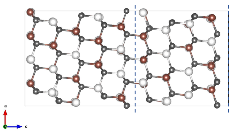
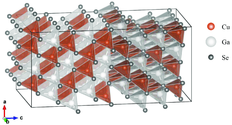
The grain boundary (GB) model consists of a supercell of 288 atoms (i.e., 72 formula units), as described in more detail further down. The dimensions of the optimized supercell are Å. We used a k-point mesh for all our GB calculations. In Fig. 1 we present a plot of the supercell model studied. The (112) planes are parallel to the -plane. Because of the periodic boundary conditions, there are two grain-boundaries. One cuts the supercell in two along the -axis, and the other is at the supercell boundaries along the same axis. As mentioned, the grain boundaries are cation-Se terminated, i.e., of type III in the terminology of Abou-Ras et al. [25]. We note that this GB is coherent (the four-fold coordination is conserved) and is stoichiometry preserving. The GB can be seen as arising from a rotation of one grain respect to the other, i.e., around an axis perpendicular to the (112) planes [32]. The rotation preserves the tetrahedral coordination of both Se and cations, but results in cation antisite pairs at the GB because it violates the periodicity of CGS along the (112) planes (this is similar to what occurs in the case of CIS). The presence of CuGa-GaCu antisite at the grain boundaries, as well as at the supercell boundaries, leads to local octet rule violations. Specifically, some Se atoms are coordinated not by two Cu and two Ga atoms, but by three (four) Cu atoms and one (no) Ga atoms, or vice versa. These have an effect on cation defect formation energies, and thus on the relative defect concentrations and on carrier density and transport, as we discuss in the next Section.
3 Results and discussion
3.1 Calculations
We first calculated the GB energy, defined as
| (1) |
where [GB] ([bulk]) is the total energy of the GB supercell (of a bulk unit cell), is (the equivalent) number of bulk unit cells contained in the GB supercell, and is the GB area [33]. We find a GB energy of 0.65 J/m2, which is slightly higher than in the case of CIS (0.42 J/m2). The value compares well with the energy of very stable twin grain boundaries in other systems. Indeed, the (111) grain boundary in SrTiO3 and the () grain boundary in -Al2O3 have reported energies of 0.52 and 0.63 Jm-2, respectively [34]. Our result is thus consistent with the fact that this type of grain boundary is common in CGS.
The band gap reduces from the bulk value of 1.68 eV to 0.47 eV at the grain boundary. Also, the valence band maximum (VBM) is displaced away from the point [to (0 0.5 0) in supercell reciprocal units], while the conductin band minimum (CBM) remains at . Similar to CIS, the band gap narrowing obeys largely to the presence of CuGa antisites. Indeed, this results in several Se atoms being coordinated by 4 Cu atoms, instead of 2. Now the valence band is known to be of dominant Cu and Se character, with important - repulsion [35]. Because the VBM itself is essentially of Se character [26, 30], a stronger - repulsion raises significantly the VBM with respect to the bulk.
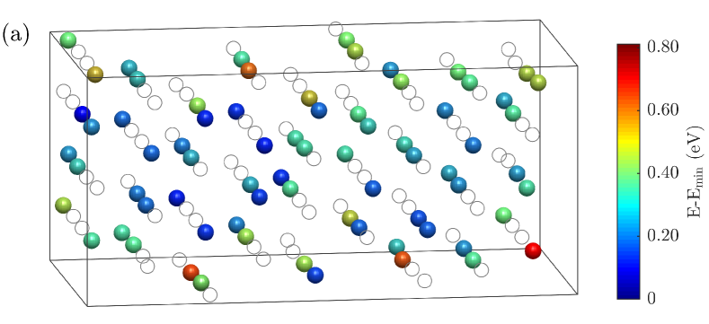
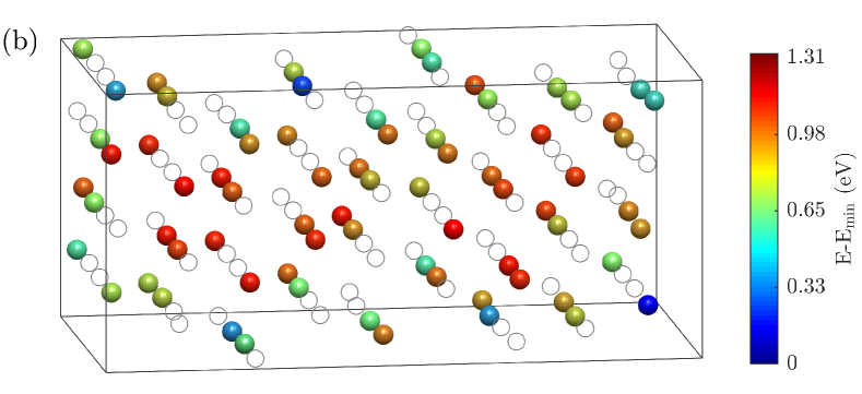
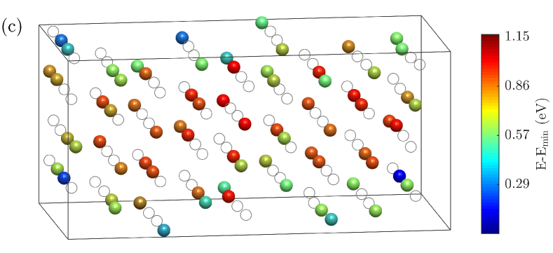
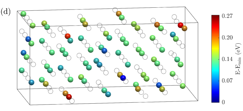
We studied the native defects VCu, GaCu, and CuGa, as well as NaCu. These appear to be the most important from the electronic properties point of view [5, 18]. Na is found in CIGS absorber layers either because of the synthesis method or because it is intentionally added [36, 37]. For a more thorough understanding of the behavior of the defects and how they affect the electronic properties of the GBs, we first determined their preferred locations in the supercell via total energy calculations, considering all 72 possible locations in each case. Figure 2 illustrates how the total energies vary as the defect changes location in the GB supercell (cf. Fig.2). In (a) the color of the spheres indicate whether a VCu located at that position has a low or high energy. The darker blue colors indicate a low total energy after relaxation, while a strong red color indicates a high total energy. The energies are referred to the lowest energy in each case. For orientation, the gray circles indicate the position of the Ga atoms (for simplicity, the Se atoms are not shown). (b) corresponds to GaCu and (d) to NaCu. (c) corresponds to CuGa, in which case the colored spheres indicate Ga atom positions and the gray circles the positions of the Cu atoms. More information on the lowest energy locations in each case is given in the Supplementary Data file.
We then calculated the formation energies of the defects in their lowest energy location. This was done following the standard procedure [38, 39]. We determined the formation energies for the defects in different charge states, and considered Ga-rich and Ga-poor growth conditions. The chemical potentials used are the same as in Ref. 30. In Fig. 3 we show the formation energies as a function of the electron chemical potential, or Fermi level, as it is commonly referred to. For a given defect, which charge state has the lowest formation energy depends on the Fermi level. This results in a lowest formation energy curve consisting of segments corresponding to different charge states, as shown by the solid lines in the plots. Fig. 3(a) corresponds to Ga-rich conditions, and Fig. 3(b) to Ga-poor conditions. The reference potential alignment and image charge correction were performed as in our previous CIS grain-boundaries study [26]. For the image charge correction the experimental dielectric constants were used [40]. For the purposes of discussion, we also present here the defect charge formation energies for bulk CGS [41]. The defect formation energies in the bulk case are plotted in Figs. 4(a) and (b), the latter corresponding to Ga-poor conditions and the former to Ga-rich conditions [42].
3.2 Discussion
Let us start by pointing out that in a material with donor and acceptor defects, in equilibrium conditions the electron chemical potential will actually be pinned to a value, , determined by overall charge neutrality [43]. A rough estimate of this energy is given by the crossing of the formation energies of the lowest donor and acceptor lines [44]. Thus, in Ga-rich conditions, in both the GB and grain interior (the bulk results being expected to correspond to the grain interior), will fall away from the band edges, implying carrier depletion and very low conductivity. This is in line with has been observed experimentally [45]. In Ga-poor conditions, on the other hand, falls at, or near, the VBM in the GB and the bulk, respectively. We can expect these to exhibit -type conductivity in such conditions. Experimentally, this is indeed known to be the case [46, 47]. Below we examine the electronic properties of the different defects indicated in the previous subsection and discuss in more detail their role in the above observations.
We consider first the Cu vacancies (VCu). The lowest energy location is at the GB. But a closer inspection of the results leading to Fig. 2 reveals that the vacancies are more likely to form at a Cu site of a normally coordinated Se atom, away from Se atoms coordinated by insufficient Ga atoms. Normally coordinated Se atoms occur of course also within the grains. Thus, we look at the formation energies in Figs. 3 and 4. These show that the VCu will form preferentially at the GB, as it has a lower formation energy by roughly 0.9 eV. Electronically, VCu is clearly a shallow acceptor in the bulk. At the GB, it may still be considered as a shallow acceptor, as its neutral-to-negative charge transition level is meV. In Ga-rich conditions, however, it will contribute little to any -type carrier density and transport, whether in the bulk or in the GB. Indeed, as indicated above, falls near the middle of the gap. Since carrier densities fall exponentially away from the band edges, they will be negligible at . In Ga-poor conditions, the GB is -type as already stated, but the contribution of VCu will be limited. This is because CuGa has a much lower formation energy in such conditions and will be the main carrier contributor. In the bulk case, one can expect VCu to be the main carrier contributing acceptor, as the other acceptor in this case (CuGa, discussed below) is somewhat deep. Note that in experiment VCu is found to be at 60 meV above the VBM [5], while our calculations find it to be at the VBM. It is possible that our calculation underestimates the defect level depth compared to experiment. A source of discrepancy might be, e.g., the charge correction scheme, which is thought to be less appropriate for shallow defects [48].
We address now GaCu. According to the results in Fig. 2, the location-energy relation of the GaCu antisites is practically anti-correlated with the graph of the VCu sites. This is because Ga preferably replaces a Cu bound to a Se atom coordinated by excess Cu atoms. Intuitively, it tends to restore the octet rule. Octet rule violations occur more frequently at the GBs and, in addition, the plots in Figs. 3 and 4 show that the formation of GaCu (comparing neutral charge states) is around 1.7 eV lower at the GB. Thus, this will be its preferred location. GaCu is a deep donor, both in the bulk and at the GBs. At the GB, in Ga-rich conditions, it is responsible for pushing away from the VBM. The behavior is essentially the same in the bulk. Thus, the GB and grain interior are practically insulating in such a conditions, which is detrimental to carrier transport and collection. This may be one of the reasons why a too high [Ga]/([In]+[Ga]) ratio is not beneficial to the efficiency of Cu(In,Ga)Se2 cells. In Ga-poor conditions, the formation energy of GaCu is too high compared to that of the other defects to have an important effect, both at the GB and in the bulk. Note that in the bulk we find the donor level to be at 365 meV from the CBM, in quite good agreement with experiment, where it is reported to be at 400 meV below the CBM [5].
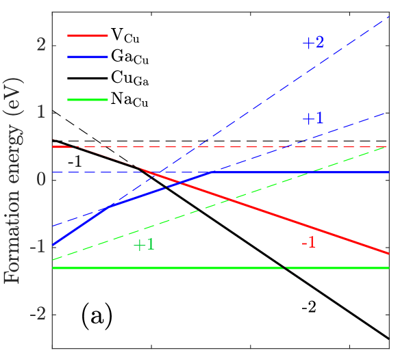
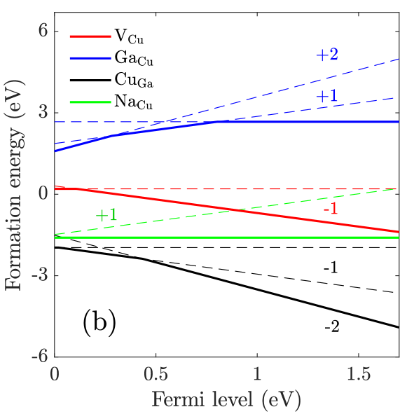
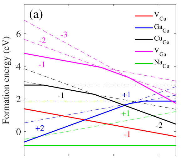
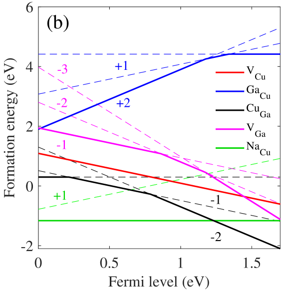
Turning to CuGa, Fig. 2 shows that its lowest energy locations correlate strongly with those of GaCu. This is not surprising since, as mentioned before, CuGa and GaCu tend to form antisite pairs at the GBs and CuGa will tend to restore the octet rule around Se atoms as well. Furthermore, its formation energy at the GB is close to 2 eV lower (comparing neutral states) than in the bulk. Thus, CuGa will also form preferentially at the GBs. This is a shallow acceptor defect at the GB. In Ga-rich conditions it will contribute to pin far from the band edges. In Ga-poor conditions, on the other hand, it is by far the leading acceptor and has the lowest formation energy overall, giving rise to a -type GB. This is consistent with has been observed in polycrystalline CuGaSe2 grown under Cu-excess [49]. In the bulk CuGa is a relatively deep acceptor. In Ga-rich conditions it will play a limited role, due to its relatively high formation energy. In Ga-poor conditions, it will contribute only secondarily to -conductivity, compared to VCu. We find that the CuGa transition levels in the bulk are meV and meV, with respect to the VBM. These can be compared with the CuGa defect levels observed in experiment in CuGaSe2 [5]. An acceptor level is observed at 60 meV above the VBM, which is assigned to a transition, and another transition at meV above the VBM, which is tentatively assigned to a transition. While the theoretical and experimental transition level values are quite off of each other (again, this is in principle a shallow level), the deep transition level values are in good agreement. This supports the intepretation given to the latter in Ref. 5.
We briefly point out that our present results for VGa in bulk CuGaSe2 support previous findings [50]. As seen in Fig. 4, VGa is a shallow acceptor in the charge state, with a high formation energy even in Ga-poor growth conditions. Our value close to 2 eV in those conditions ( eV ) is comparable to the value of 2.5 eV in Ref. 50, calculated in somewhat less Ga-poor growth conditions ( eV). Due to this, VGa does not have a significant effect on the electronic properties of CuGaSe2. This is expected to remain so in GBs, and we did not study VGa in GBs.
Finally, we consider the case of NaCu impurities. The analysis of the results in Fig. 2 indicates that these occur more commonly at the GBs. Also, the formation energy of NaCu (neutral state) is lower at the GB by 0.45 eV. At the GBs, in Ga-rich conditions, although its ground state is neutral, it will still contribute to compensate the acceptor defects because the formation energy of its +1 charge state is sufficiently low in the lower half of the band gap. In Ga-poor conditions, it will tend to play the same role, but less efficiently, as its formation energy is somewhat higher than the donor in that case (CuGa). This is in contrast with the case of CIS, where at the GBs NaCu impurities clearly tend to passivate any donors and can even contribute to type inversion [26]. It must be pointed out, however, that theoretical calculations suggest that NaCu can give rise to a neutral hole-barrier at GBs in CIGS compounds, resulting from its lack of -states compared to Cu [26, 51], an effect indeed observed in CuGaSe2 [52]. Thus, NaCu at the GB can be expected to be overall slightly beneficial. In the bulk case, in Ga-rich conditions NaCu will not alter significantly the -type vs. -type carrier balance, so it will remain carrier depleted. In Ga-poor conditions, NaCu will tend to passivate any acceptor. This is detrimental, of course, to the intended -type conductivity of the bulk. But its negative impact will be mitigated, as Na is expected to segregate to the GBs, where it can have a beneficial effect.
4 Conclusions and outlook
Our first-principles computational study of cation-Se 3 (112) grain boundaries in CuGaSe2 shows that the native defects VCu, GaCu, and CuGa and the impurity NaCu have a formation energy at the GBs that is lower than in the grain interiors. Thus, they will have a higher concentration at the GBs. With respect to their effect on electronic properties, we find that in Ga-rich growth conditions VCu and the antisites GaCu and CuGa are mainly responsible for having pinned toward the middle of the gap, resulting in carrier depletion. But in Ga-poor growth conditions, the formation energies of VCu and GaCu are high and do not influence significantly the carrier density or the position of , while CuGa locates the latter near the VBM and gives rise to a -type grain boundary. Furthermore, NaCu will be in its neutral state, and while in Ga-rich conditions its state still contributes to pin toward the middle of the gap, in Ga-poor conditions its effect is weak and will fail to passivate the CuGa defects and prevent recombination at the grain boundary, in contrast with its effect in CuInSe2 GBs. However, it is still expected to act as a neutral hole barrier due to its band bending effect at the GBs. As regards bulk CuGaSe2, we find that VCu is a shallow donor, while in experiment it is found to be 60 meV above the VBM. On the other hand, we find that GaCu is a deep donor, 365 meV below the CBM, which compares well with the experimental value of 400 meV. Also, for CuGa we find a deep transition level at 790 meV above the VBM, supporting the interpretation given to the level meV above the VBM observed in experiment. Finally, we find that NaCu tends to have a detrimental effect on the carrier density, both in Ga-rich and Ga-poor conditions, but greatly mitigated because it will typically segregate to the GBs and have a low density in the grain interiors.
There are several paths that future work can take. Here we have considered a set of defects that affect critically the electronic properties of GBs in CuGaSe2, and thus of the absorber layer as a whole. But there are other types of defects that can be considered as well. In CIGS absorber layers, for instance, depending to an extent on the synthesis method, potassium and heavier alkali impurities can be present [8], or carbon [53] and oxygen [54]. Moreover, such defects can be present at the interfaces between the absorber layer and the substrate or buffer layers, with important effect on carrier passivation/transport. The effects of such impurities have been studied computationally mainly in CuInSe2 so far [55, 56, 57]. It will be important that future work considers them in CuGaSe2 as well.
Acknowledgments
We acknowledge the financial support of FWO-Vlaanderen through project G.0150.13 The computational resources and services used in this work were provided by the VSC (Flemish Supercomputer Center) and the HPC infrastructure of the University of Antwerp (CalcUA), both funded by FWO-Vlaanderen and the Flemish Government-department EWI.
References
- [1] T. Plirdpring, K. Kurosaki, A. Kosuga, T. Day, S. Firdosy, V. Ravi, G. J. Snyder, A. Harnwunggmoung, T. Sugahara, Y. Ohishi, H. Muta, and S. Yamanaka, Adv. Mater. 24 (2012) 3622.
- [2] A. Raevskaya, O. Rozovik, A. Novikova, O. Selyshchev, O. Stroyuk, V. Dzhagan, I. Goryacheva, N. Gaponik, D. R. T. Zahn, and A. Eychmüller, RSC Adv. 8 (2018) 7550.
- [3] J.-H. Kim, S.-Y. Yoon, K.-H. Kim, H.-B. Lim, H.-J. Kim, and H. Yang, Opt. Lett. 43 (2018) 5287.
- [4] T. D. Lee and A. U. Ebong, Renew. Sust. Energ. Rev. 70 (2018) 1286.
- [5] C. Spindler, F. Babbe, M. H. Wolter, D. Ehré, K. Santhosh, P. Hilgert, F. Werner, and S. Siebentritt, Phys. Rev. Mat. 3 (2019) 090302.
- [6] S. Ishizuka, Phys. Status Solidi A 216 (2019) 1800873.
- [7] S. Ishizuka, A. Yamada, P. J. Fons, H. Shibata and S. Niki, Prog. Photovolt: Res. Appl. 22 (2014) 821.
- [8] P. Jackson, R. Wuerz, D. Hariskos, E. Lotter, W. Witte and M. Powalla, Phys. Status Solidi RRL 10 (2016) 583.
- [9] V. Nadenau, U. Rau, A. Jasenek, and H. W. Schock, J. Appl. Phys. 87 (2000) 584.
- [10] X. Hu, J. Xue, J. Tian, G. Weng and S. Chen, Appl. Optics 56 (2017) 4090.
- [11] J.-H. Wi, W. S. Han, W.-J. Lee, D.-H. Cho, H.-J. Yu, C.-W. Kim, C. Jeong, J. H. Yun, C.-I. Kim and Y.-D. Chung, IEEE J. Photovolt. 8 (2018) 840.
- [12] Y. Wei, D. Zhuang, M. Zhao, N. Zhang, X. Yu, R. Sun, L. Zhang, X. Lyu, X. Peng and J. Wei Mater. Lett. 230 (2018) 128.
- [13] Wide-gap chalcopyrites, S. Siebentritt and U. Rau, Eds. (Springer, Berlin, 2006).
- [14] S. Jung and J. Kim, J. Nanosci. Nanotechno. 16 (2016) 5279.
- [15] S. Ullah, M. Mollar and B. Mar’ı, J. Solid State Electrochem. 20 (2016) 2251.
- [16] A. Popp and C. Pettenkofer, Appl. Surf. Sci. 416 (2017) 815.
- [17] M. A. Awaah, U. Obahiagbon, H. Mohammed, O. Akpa, I. Awaah, T. Isaac-Smith, N. Korivi, J. B. Posthill and K. Das, Cogent Engineering 5 (2018) 1514941.
- [18] S. Siebentritt, M. Igalson, C. Persson and S. Lany, Prog. Photovolt: Res. Appl. 18 (2010) 390.
- [19] J. Bekaert, R. Saniz, B. Partoens, and D. Lamoen, J. Appl. Phys. 117 (2015) 015104.
- [20] C. Spindler, D. Regesch and S. Siebentritt, Appl. Phys. Lett. 109 (2016) 032105.
- [21] M. M. Islam, S. Wang, S. Ishizuka, H. Shibata, S. Niki, K. Akimoto and T. Sakurai, Jpn. J. Appl. Phys. 57 (2018) 08RC02.
- [22] S. Sadewasser, D. Abou-Ras, D. Azulay, R. Baier, I. Balberg, D. Cahen, S. Cohen, K. Gartsman, K. Ganesan, J. Kavalakkatt, W. Li, O. Millo, Th. Rissom, Y. Rosenwaks, H.-W. Schock, A. Schwarzman and T. Unold, Thin Solid Films 519 (2011) 7341.
- [23] S. S. Schmidt, D. Abou-Ras, S. Sadewasser, W. Yin, Ch. Feng and Y. Yan, Phys. Rev. Lett. 109 (2012) 095506.
- [24] U. Rau, K. Taretto and S. Siebentritt, Appl. Phys. A 96 (2009) 221.
- [25] D. Abou-Ras, B. Schaffer, M. Schaffer, S. S. Schmidt, R. Caballero and T. Unold, Phys. Rev. Lett. 108 (2012) 075502.
- [26] R. Saniz, J. Bekaert, B. Partoens and D. Lamoen, Phys. Chem. Chem. Phys. 19 (2017) 14770.
- [27] G. Kresse and J. Furthmüller, Phys. Rev. B 54 (1996) 11169.
- [28] G. Kresse and D. Joubert, Phys. Rev. B 59 (1999) 1758.
- [29] J. P. Perdew, K. Burke and M. Ernzerhof, Phys. Rev. Lett. 77 (1996) 3865.
- [30] J. Bekaert, R. Saniz, B. Partoens and D. Lamoen, Phys. Chem. Chem. Phys. 16 (2014) 22299.
- [31] See www.vasp.at/wiki/.
- [32] D. Abou-Ras, S. Schorr and H. W. Schock, J. Appl. Cryst. 40 (2007) 841.
- [33] W. Körner, P. D. Bristowe, and C. Elsässer, Phys. Rev. B 84, 045305 (2011).
- [34] S. Hutt, S. Köstlmeier and C. Elsässer, J. Phys.: Condens. Matter 13 (2001) 3949.
- [35] J. E. Jaffe and A. Zunger, Phys. Rev. B 28 (1983) 5822.
- [36] L. Kronik, D. Cahen and H. W. Schock, Adv. Mater. 10 (1998) 31.
- [37] A. Rockett, Thin Solid Films 480 (2005) 2.
- [38] S. B. Zhang and J. E. Northrup, Phys. Rev. Lett. 67 (1991) 2339.
- [39] C. G. Van de Walle and J. Neugebauer, J. Appl. Phys. 95 (2004) 3851.
- [40] N. N. Syrbu, M. Bogdanash, V. E. Tezlevan and I. Mushcutariu, Physica B 299 (1997) 199.
- [41] These are qualitatively the same as in Ref. 30, but there are quantitative differences because of a sign error in the potential alignment in that paper.
- [42] Note that Ga vacancies (VGa) are also considered further down in the case of the bulk. This is for completeness and for comparison with previous work reported in Ref. 30.
- [43] S. M. Sze and K. K. Ng, Physics of semiconductor devices (John Wiley & Sons, Hoboken, 2007).
- [44] The self-consistently calculated value corresponding to Ga-rich and Ga-poor conditions is given for bulk CGS in the Supplementary Data file.
- [45] A. Gerhard, W. Harneit, S. Brehme, A. Bauknecht, U. Fiedeler, M.Ch. Lux-Steiner and S. Siebentritt, Thin Solid Films 387 (2001) 67.
- [46] J. H. Schön, Ch. Kloc and E. Bucher, Thin Solid Films 361 (2000) 411.
- [47] S. Siebentritt and S. Schuler, J. Phys. Chem. Solids 64 (2003) 1621.
- [48] C. Persson, Y.-J. Zhao, S. Lany and A. Zunger, Phys. Rev. B 72 (2005) 035211.
- [49] S. Schuler, S. Nishiwaki, J. Beckmann, N. Rega, S. Brehme, S. Siebentritt and M.C. Lux-Steiner, Proceedings of the 29th IEEE Photovoltaic Specialist Conference (New Orleans, 2002) p. 504.
- [50] J. Pohl and K. Albe, Phys. Rev. B 87 (2013) 245203.
- [51] C. Persson and A. Zunger, Phys. Rev. Lett. 91 (2003) 266401.
- [52] S. Siebentritt, S. Sadewasser, M. Wimmer, C. Leendertz, T. Eisenbarth and M, Ch. Lux-Steiner, Phys. Rev. Lett. 97 (2006) 146601.
- [53] C. J. Hibberd, E. Chassaing, W. Liu, D. B. Mitzi, D. Lincot, and A. N. Tiwari, Prog. Photovolt.: Res. Appl. 18 (2010) 434.
- [54] X. Niu, H. Zhu, X. Liang, Y. Guo, Z. Li, Y. Mai, Appl. Surf. Sci. 426 (2017) 1213.
- [55] H. Xiao and W. A. Goddard III, J. chem. Phys. 141 (2014) 094701.
- [56] S. K. Sahoo, R. K. M. Raghupathy, T. D. Kühne, H. Mirhosseini, J. Phys. Chem. C 122 (2018) 21202.
- [57] D. Music and Ph. Keuter, Solid State Commun. 299 (2019) 113652.