Contacts and upstream modes explain the electron-hole asymmetry in the graphene quantum Hall regime
Abstract
Observations of electron-hole asymmetry in transport through graphene devices at high magnetic field challenge prevalent models of the graphene quantum Hall effect. Here, we study this asymmetry both in conventional magnetotransport and in scanning gate microscopy maps measured in an encapsulated graphene constriction. We reveal that the presence of upstream modes and local doping in the vicinity of electrical contacts leads to a totally different picture of topological breakdown for electrons and holes, explaining the observed asymmetry.
Injecting and collecting charges in two-dimensional electronic systems (2DESs) through ohmic contacts look like easy tasks, with most models describing contacts as smooth extensions of the 2DES. However, in the quantum Hall (QH) regime, the topic is far from trivial as charge carriers flow in different topologically-protected quantum Hall edge channels (QHECs). Indeed, good coupling of these channels with the contacts involve no backscattering of incoming QHECs and perfect equilibration in the injection of carriers in the different outgoing QHECs. Fulfilling these two criteria proves difficult because of the complex interface between the metallic contacts and the 2DES Komiyama and Hirai (1989); Dahlem et al. (2010); Weis and von Klitzing (2011).
In the graphene QH regime, the situation is even more cumbersome, for two reasons at least. First, state-of-the-art QH devices rely on graphene encapsulation in hexagonal boron nitride (hBN) and on one-dimensional line-contacts obtained by depositing metal on the flanks of the device Wang et al. (2013). Such abrupt metal-graphene contact was shown to potentially destroy electron-hole symmetry Khomyakov et al. (2010). Second, different experimental results indicate that upstream (i.e. counterpropagating) QHECs can flow along device edges Cui et al. (2016); Marguerite et al. (2019); Moreau et al. (2020). The most common explanation ascribes their coexistence to an inhomogeneous screening of the back gate potential, related to fringing fields, leading to charge carriers accumulation at device borders Silvestrov and Efetov (2008).
Thanks to scanning gate microscopy (SGM), topological breakdown of the QH effect has recently been shown to originate from the coupling of up- and downstream QHECs along the very same edge in this material Marguerite et al. (2019); Moreau et al. (2020). In particular, we showed that the coupling is achieved through the localized states of antidots located along the edges Moreau et al. (2020). Importantly, the latter SGM experiments have essentially focused on hole-type charge carriers and evidences for the same mechanisms for electron-type charge carriers remain elusive.
In this letter, we combine transport and SGM with tight-binding simulations to study the topological breakdown of graphene QHECs in the case of electrons and holes. Our results reveal that contacts lead to a different spatial configuration of upstream QHECs for both types of charge carriers. This asymmetry is at the origin of distinct mechanisms causing a topological breakdown on the electron and hole sides.
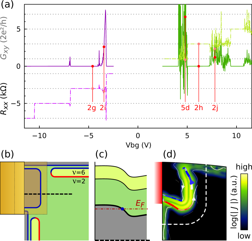
The studied sample, depicted in Fig. 1a, consists in a monolayer of graphene encapsulated between two hBN flakes Terrés et al. (2016). The longitudinal resistance is measured via line contacts made of gold deposited on a thin adhesion layer of chromium Wang et al. (2013). Inherently to this contact layout, they overlap the heterostructure. Charge carrier density is varied using a back gate voltage and a magnetic field is applied perpendicularly to the graphene plane. We furthermore use a sharp metallic SGM tip, biased at a voltage to change locally the charge carrier density.
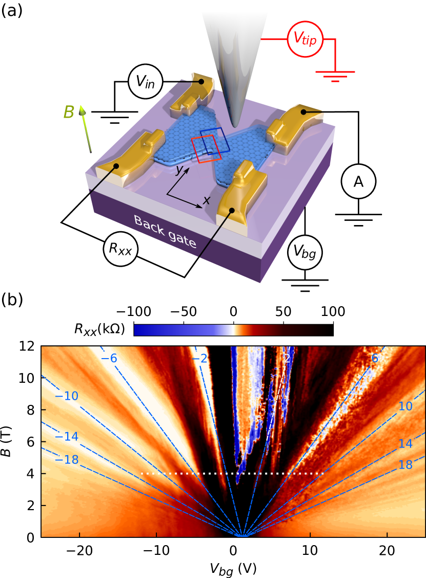
A fan diagram is presented in Fig. 1b. The white stripes correspond to vanishing and indicate that QHECs are topologically protected, so that charge carriers backscattering is forbidden. At low positive and above T, exhibits extremely large and irregular fluctuations. Such an asymmetric and perturbed behavior has already been reported in Amet et al. (2015) and is relatively common in the case of encapsulated graphene devices. In order to stand at the verge of this regime, we limit our measurements to T in the remainder of this paper. as a function of is shown in Fig. 2a for this value of magnetic field.
SGM maps, obtained by recording as a function of the tip position, reveal precious information on the origin of the coupling between QHECs. The tip perturbation locally tunes the coupling and, hence, the backscattering between QHECs Hackens et al. (2010); Martins et al. (2013); Marguerite et al. (2019); Moreau et al. (2020); Paradiso et al. (2011); Pascher et al. (2014). In turn, this leads to concentric fringes of (local maxima or minima) in the SGM map, centered on the spot where the coupling occurs. As shown in Fig. 2b, SGM contrasts is located along edges for holes. It is coherent with former studies that ascribed these signatures to the presence of upstream QHECs, coupled with the downstream modes flowing along the same edge Moreau et al. (2020); Marguerite et al. (2019). For electrons, however, SGM contrast is centered only in the constriction region, as indicated with SGM fringes with higher in Fig. 2c and with spots of lower in Fig. 2d. Contrary to the hole case, no contrast is found centered on the edges of the device. It is noteworthy that similar signatures have been found in SGM experiments on classical semiconductor-based 2DESs Hackens et al. (2010); Martins et al. (2013), where there is no upstream QHEC. In these systems, topological breakdown was assigned to the presence of an antidot located in the vicinity of the constriction and coupling the QHECs running at the opposite device edges.
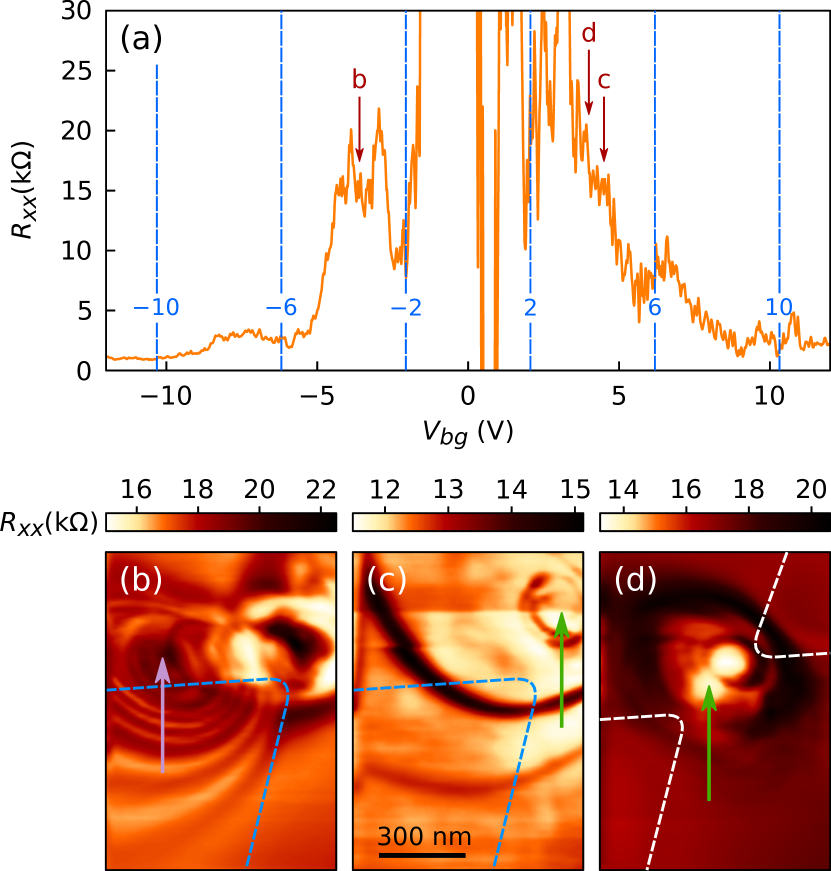
As a first hypothesis to account for electron-hole asymmetry, one could speculate that upstream QHECs only exist for holes. Impurities and defects along the borders could in this case favor holes accumulation and induce such charge asymmetry, as proposed by Marguerite et al. Marguerite et al. (2019) (referred to hereafter as the “impurity model”). While our data can not undoubtedly discard this scenario, the impurity model alone fails to yield a full picture of QHECs in graphene in regards to other experimental results reported in the literature Cui et al. (2016) (see supplemental materials). On the other hand the mainstream theory, namely the inhomogeneous screening of the backgate potential (the fringing field model), predicts the emergence of upstream QHECs both for holes and electrons, and consequently an apparent charge symmetry. In the following, we show that electron-hole asymmetry can also be explained in the fringing field model framework.
In the model that we develop hereafter, we assume that charge carriers accumulate along the edges in the same way on the electron and hole sides. The bending of energy bands leads in both cases to the presence of upstream QHECs. In this scenario, electron-hole asymmetry originates from the contacts. In particular, the difference of work-function between graphene and chromium, forming the adhesion layer of contacts, yields a hole-type doping below the metallic regions overlapping the stack illustrated in Fig. 3a. The work-function-induced difference of the potential (see supplemental materials) can be approximated by Giovannetti et al. (2008); Chaves et al. (2014)
| (1) |
where eV Waldrop (1984) and eV Giovannetti et al. (2008) are the work-functions of chromium and graphene respectively and with nm the vertical distance between graphene and the overlapping metal, the hBN permittivity and m/s the Fermi velocity of graphene. With these data, we find eV. As a result, charge carrier density is larger below the overlapping metal, with respect to the bulk, when the bulk is doped with holes, whereas it is smaller for an electron-doped bulk.
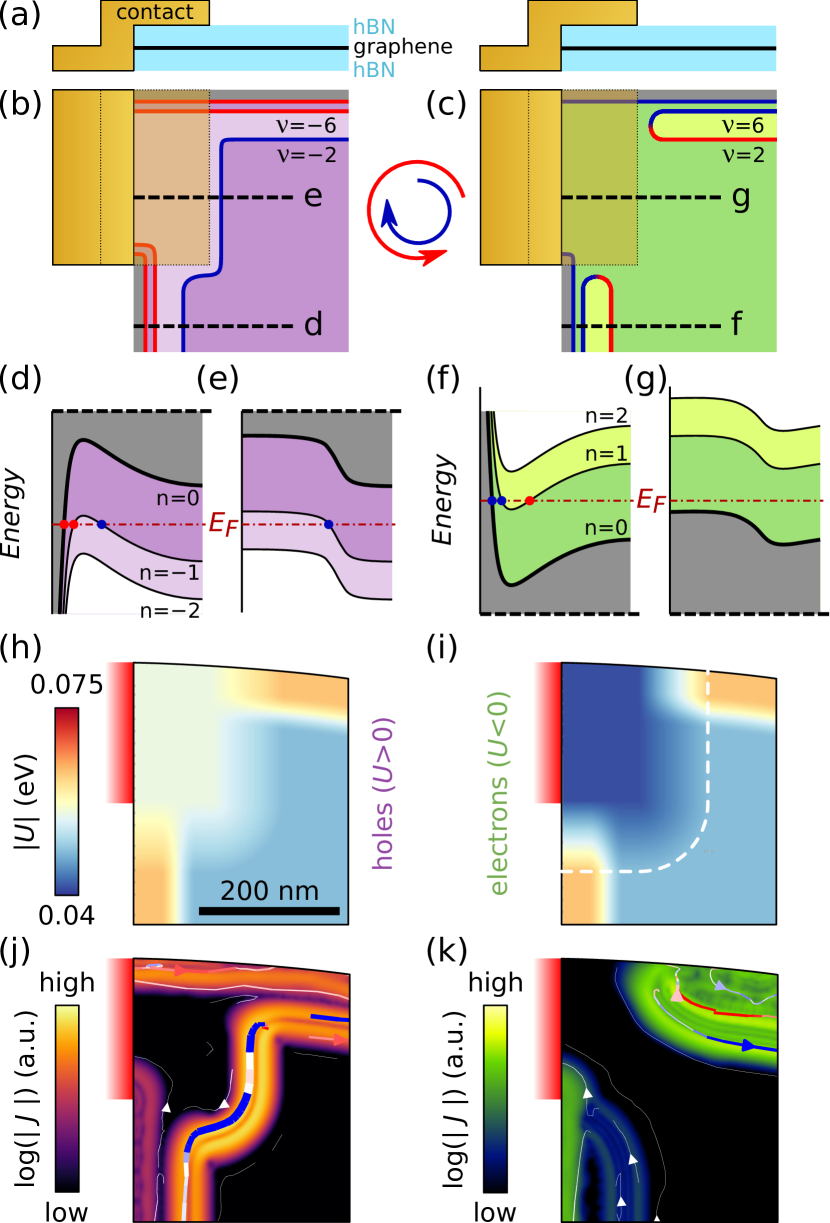
In the QH regime, this modulation of charge carrier density has an important influence on the QHECs spatial configuration in the vicinity of the contacts, which differs for holes and electrons, as illustrated in Figs. 3b,c. In this schematic, upstream QHECs flow along the edges where one of the bent Landau levels crosses twice the Fermi energy, as shown in Fig. 3d for holes and 3f for electrons. However, this picture is no longer valid around and below the contacts pads, i.e., in the doped orange-shaded region in Fig. 3b-c. For holes, the inner (clockwise) QHEC circumvent the contact zone, due to the increase of holes density (Fig. 3e). For electrons, the lower charge density close to the contacts (Fig. 3g) leads to the merging of the inner (counterclockwise) with the closest clockwise QHECs (Fig. 3c). These QHECs are therefore perfectly equilibrated.
Based on this model, we performed tight-binding simulations, using the KWANT package Groth et al. (2014). Maps of the absolute value of the on-site potential around the contacts are shown in Fig. 3h for holes and in Fig. 3i for electrons. They feature an increase of charge carrier density along the edges, proportional to the bulk density (see supplemental materials), in addition to a constant positive offset energy eV (Eq. (1)) around the contacts. The resulting current density maps are presented in Figs. 3j,k. The QHECs are visible in lighter tones and match the qualitative picture of Figs. 3b,c.
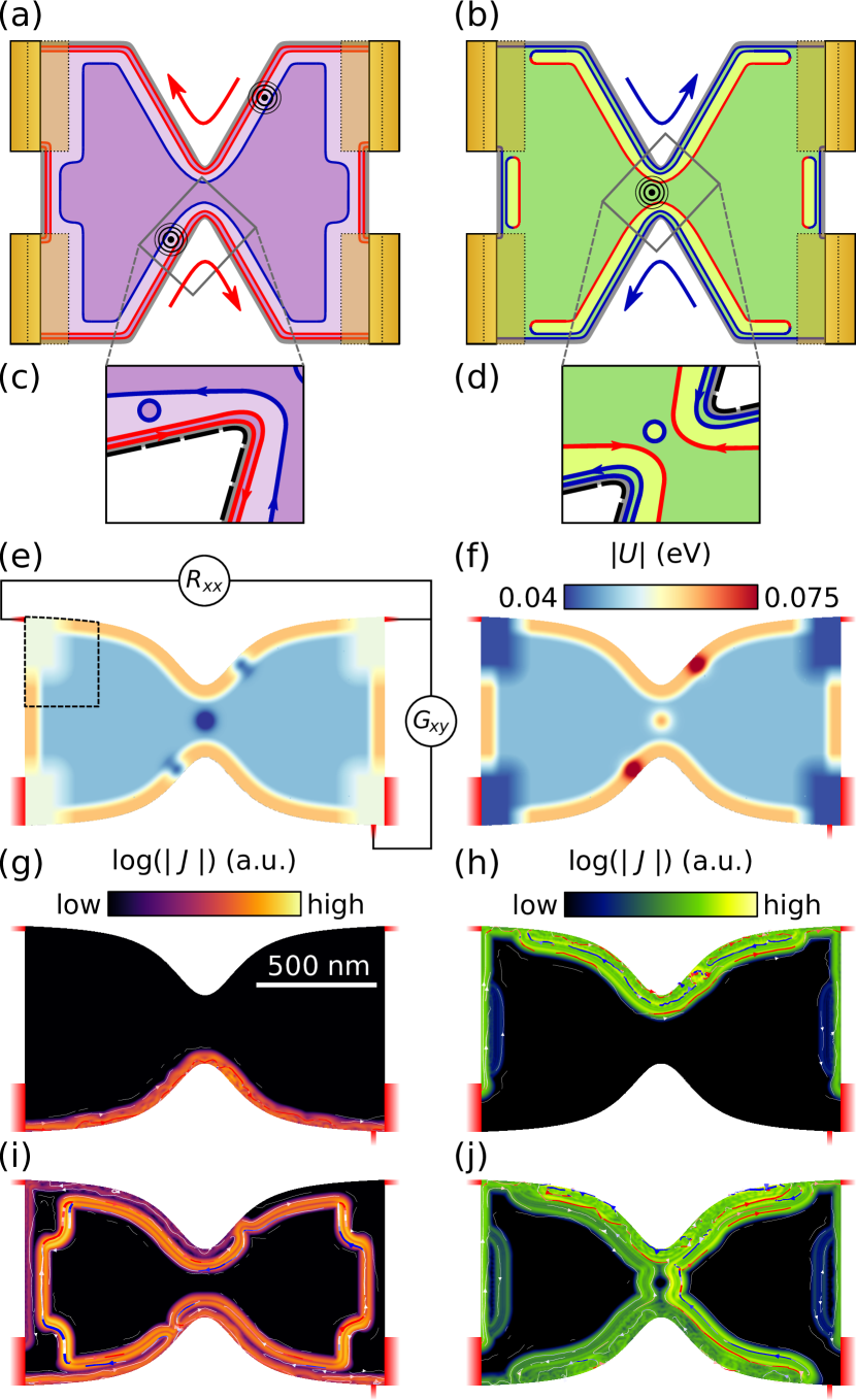
We now consider the entire sample to examine the consequences of these different QHECs spatial configurations at the contacts for holes and electrons, and the relationship with the experimental data of Fig. 2. For holes (left side of Fig. 4), it appears that the inner QHEC (blue) forms a closed loop, as illustrated in Fig. 4a. In the absence of coupling with the outer QHECs (red), this loop is topologically equivalent to a localized state in QH theory since it is not directly coupled with contacts and should not influence transport. The effective filling factor of the system is therefore given by the region outside the loop (here , in light purple). To observe the topological breakdown of QHECs, holes running along one of the sample edges should be backscattered to the opposite edge. This can only be achieved by coupling the upstream QHEC loop both on the upper and lower sides of the sample, for example at locations pinpointed by concentric black circles in Fig. 4a. The SGM contrast highlighted along the sample edge in Fig. 2b is therefore the signature of one of the two coupling spots between upstream QHECs. In particular, the coupling is achieved through an antidot, as depicted in Fig. 4c Moreau et al. (2020). By introducing these antidots in the simulated potential landscape, with Gaussian functions centered close to the edges (see the potential map in Fig. 4e), we correctly capture the mechanism leading to holes backscattering. Fig. 4g shows a simulated current density map where propagating QHECs are not coupled through the antidots. This is in stark contrast with Fig. 4i where coupling is achieved at a slightly different value of (calculated from ), so that holes flow through the inner QHEC loop, connecting both edges.
For electrons (right side of Fig. 4), the equilibrated QHECs form loops running along the edges, as illustrated in Fig. 4b. Contrary to holes, the effective filling factor of the system is given by the bulk (here , in dark green), as for conventional semiconductor-based 2DEGs. The topological breakdown of QHECs can only be achieved by coupling the upstream QHECs of the upper and lower sides of the sample, which can only happen in the vicinity of the constriction, as illustrated with concentric black circles in Fig. 4b. Electrons running along one of the edges (in a QHEC loop) can then be backscattered to the opposite side of the device. The SGM contrast highlighted at the center of the constriction in Figs. 2c-d is therefore the consequence of the coupling between the opposite QHECs loops through an antidot located at the center of the constriction, as depicted in Fig. 4d Hackens et al. (2010). Simulations support this picture, when introducing an antidot at the center of the constriction (Fig. 4f). Fig. 4h depicts a current density map where QHECs loops are visible along the edges but the absence of coupling with the opposite edge prevents backscattering. When coupling is active (at different , as in Fig. 4j), electrons flow from one edge to the other through the central antidot and can be backscattered.
The simulated and curves as a function of , obtained in this system, are presented in Fig. 5a for holes (purple) and electrons (green). When is zero, exhibits the expected plateaus for graphene at . Non-zero , accompanied by the transition between two Hall plateaus, indicates the coupling between the opposite device edges (as shown in Fig. 4) and the non-zero probability for charge carriers to be back-scattered. A striking feature of the curve is the presence of large fluctuations on the electron side, similarly to the experimental data presented in Fig. 2a. These fluctuations originate from extra QHECs running below the contacts, inducing a direct backscattering of charge carriers in the contact area (Figs. 5b,c). This mechanism prevents a proper equilibration between the propagating QHECs and the contacts. In addition, current injection is strongly hampered in this situation, preventing proper determination of . Parasitic doping below the contacts therefore explains measurements artifacts such as the large variation of resistance even towards negative values reported here (Fig. 2a) as well as in previous experiments Amet et al. (2015).
In summary, we have highlighted that line contacts, used for state-of-the-art encapsulated graphene samples, can lead to different spatial configurations of the upstream QHECs on the electron and hole sides. This yields distinct mechanisms at the origin of the QH topological breakdown for both charge carriers types. For holes, the breakdown occurs by coupling the upstream QHECs through antidots located at the device edges whereas for electrons, all the QHECs running along the same edge are equilibrated and the breakdown occurs through the bulk, similar to conventional semi-conductor 2DEGs. This interpretation is in full agreement with microwave impedance microscopy results, where the QH topological breakdown was shown to coincide either with a conducting bulk, either with conducting edges, depending on the charge carriers type Cui et al. (2016). Our conclusions pinpoint the importance of considering the influence of contacts when designing two-dimensional materials-based samples, in particular when these contacts are to be coupled with topologically protected edge channels.
Acknowledgements.
The authors thank Samuel Dechamps and Jean-Christophe Charlier for discussion about metal-graphene interaction. This work was partly funded by the Federation Wallonie-Bruxelles through the ARC Grant No. 16/21-077, by the F.R.S-FNRS through the Grant No. J008019F, and from the European Union’s Horizon 2020 Research and Innovation program (Core 1 No. 696656 and Core 2 No. 785219). This work was also partly supported by the FLAG-ERA grant TATTOOS, through F.R.S.-FNRS PINT-MULTI grant No. R 8010.19. B.B. (research assistant), B.H. (research associate) and N.M. (FRIA fellowship) acknowledge financial support from the F.R.S.-FNRS of Belgium. Support by the Helmholtz Nanoelectronic Facility (HNF), the EU ITN SPINOGRAPH and the DFG (SPP-1459) is gratefully acknowledged. K.W. and T.T. acknowledge support from the Elemental Strategy Initiative conducted by the MEXT, Japan ,Grant Number JPMXP0112101001, JSPS KAKENHI Grant Numbers JP20H00354 and the CREST(JPMJCR15F3), JST.References
- Komiyama and Hirai (1989) S. Komiyama and H. Hirai, Phys. Rev. B 40, 7767 (1989).
- Dahlem et al. (2010) F. Dahlem, E. Ahlswede, J. Weis, and K. v. Klitzing, Phys. Rev. B 82, 121305(R) (2010).
- Weis and von Klitzing (2011) J. Weis and K. von Klitzing, Philosophical Transactions of the Royal Society A 369, 3954 (2011).
- Wang et al. (2013) L. Wang, I. Meric, P. Y. Huang, Q. Gao, Y. Gao, H. Tran, T. Taniguchi, K. Watanabe, L. M. Campos, D. A. Muller, J. Guo, P. Kim, J. Hone, K. L. Shepard, and C. R. Dean, Science 342, 614 (2013).
- Khomyakov et al. (2010) P. A. Khomyakov, A. A. Starikov, G. Brocks, and P. J. Kelly, Phys. Rev. B 82, 115437 (2010).
- Cui et al. (2016) Y.-T. Cui, B. Wen, E. Y. Ma, G. Diankov, Z. Han, F. Amet, T. Taniguchi, K. Watanabe, D. Goldhaber-Gordon, C. R. Dean, and Z.-X. Shen, Phys. Rev. Lett. 117, 186601 (2016).
- Marguerite et al. (2019) A. Marguerite, J. Birkbeck, A. Aharon-Steinberg, D. Halbertal, K. Bagani, I. Marcus, Y. Myasoedov, A. K. Geim, D. J. Perello, and E. Zeldov, Nature 575, 628 (2019).
- Moreau et al. (2020) N. Moreau, B. Brun, S. Somanchi, K. Watanabe, T. Taniguchi, C. Stampfer, and B. Hackens, to be precised none, none (2020).
- Silvestrov and Efetov (2008) P. G. Silvestrov and K. B. Efetov, Phys. Rev. B 77, 155436 (2008).
- Terrés et al. (2016) B. Terrés, L. A. Chizhova, F. Libisch, J. Peiro, D. Jörger, S. Engels, A. Girschik, K. Watanabe, T. Taniguchi, S. V. Rotkin, J. Burgdörfer, and C. Stampfer, Nature Communications 7, 11528 (2016).
- Amet et al. (2015) F. Amet, A. J. Bestwick, J. R. Williams, L. Balicas, K. Watanabe, T. Taniguchi, and D. Goldhaber-Gordon, Nature Communications 6, 5838 (2015).
- Hackens et al. (2010) B. Hackens, F. Martins, S. Faniel, C. Dutu, H. Sellier, S. Huant, M. Pala, L. Desplanque, X. Wallart, and V. Bayot, Nature Communications 1, 39 (2010).
- Martins et al. (2013) F. Martins, S. Faniel, B. Rosenow, H. Sellier, S. Huant, M. G. Pala, L. Desplanque, X. Wallart, V. Bayot, and B. Hackens, Scientific Reports 3, 1416 (2013).
- Paradiso et al. (2011) N. Paradiso, S. Heun, S. Roddaro, D. Venturelli, F. Taddei, V. Giovannetti, R. Fazio, G. Biasiol, L. Sorba, and F. Beltram, Phys. Rev. B 83, 155305 (2011).
- Pascher et al. (2014) N. Pascher, C. Rössler, T. Ihn, K. Ensslin, C. Reichl, and W. Wegscheider, Phys. Rev. X 4, 011014 (2014).
- Giovannetti et al. (2008) G. Giovannetti, P. A. Khomyakov, G. Brocks, V. M. Karpan, J. van den Brink, and P. J. Kelly, Phys. Rev. Lett. 101, 026803 (2008).
- Chaves et al. (2014) F. A. Chaves, D. Jiménez, A. W. Cummings, and S. Roche, Journal of Applied Physics 115, 164513 (2014).
- Waldrop (1984) J. R. Waldrop, Journal of Vacuum Science & Technology B 2, 445 (1984).
- Groth et al. (2014) C. W. Groth, M. Wimmer, R. A. Akhmerov, and X. Waintal, New J. Phys. 26, 063065 (2014).