Supplementary Information: Coherent coupling between vortex bound states and magnetic impurities in 2D layered superconductors
Sunghun Park
Departamento de Física Teórica de la Materia Condensada, Instituto Nicolás Cabrera and Condensed Matter Physics Center (IFIMAC), Universidad Autónoma de Madrid, E-28049 Madrid,
Spain
Víctor Barrena
Laboratorio de Bajas Temperaturas y Altos Campos Magnéticos, Departamento de Física de la Materia Condensada, Instituto Nicolás Cabrera and Condensed Matter Physics Center (IFIMAC), Unidad Asociada UAM-CSIC, Universidad Autónoma de Madrid, E-28049 Madrid,
Spain
Samuel Mañas-Valero
Instituto de Ciencia Molecular (ICMol), Universidad de Valencia, Catedrático José Beltrán 2, 46980 Paterna, Spain
José J. Baldoví
Instituto de Ciencia Molecular (ICMol), Universidad de Valencia, Catedrático José Beltrán 2, 46980 Paterna, Spain
Max Planck Institute for the Structure and Dynamics of Matter, Luruper Chaussee 149, D-22761 Hamburg, Germany
Antón Fente
Laboratorio de Bajas Temperaturas y Altos Campos Magnéticos, Departamento de Física de la Materia Condensada, Instituto Nicolás Cabrera and Condensed Matter Physics Center (IFIMAC), Unidad Asociada UAM-CSIC, Universidad Autónoma de Madrid, E-28049 Madrid,
Spain
Edwin Herrera
Laboratorio de Bajas Temperaturas y Altos Campos Magnéticos, Departamento de Física de la Materia Condensada, Instituto Nicolás Cabrera and Condensed Matter Physics Center (IFIMAC), Unidad Asociada UAM-CSIC, Universidad Autónoma de Madrid, E-28049 Madrid,
Spain
Federico Mompeán
Instituto de Ciencia de Materiales de Madrid, Consejo Superior de Investigaciones Científicas (ICMM-CSIC), Sor Juana Inés de la Cruz 3, 28049 Madrid, Spain
Mar García-Hernández
Instituto de Ciencia de Materiales de Madrid, Consejo Superior de Investigaciones Científicas (ICMM-CSIC), Sor Juana Inés de la Cruz 3, 28049 Madrid, Spain
Ángel Rubio
Max Planck Institute for the Structure and Dynamics of Matter, Luruper Chaussee 149, D-22761 Hamburg, Germany
Nano-Bio Spectroscopy Group and European Theoretical Spectroscopy Facility (ETSF), Universidad del País Vasco CFM CSIC-UPV/EHU-MPC & DIPC, Avenida Tolosa 72, 20018 San Sebastián, Spain
Eugenio Coronado
Instituto de Ciencia Molecular (ICMol), Universidad de Valencia, Catedrático José Beltrán 2, 46980 Paterna, Spain
Isabel Guillamón
Laboratorio de Bajas Temperaturas y Altos Campos Magnéticos, Departamento de Física de la Materia Condensada, Instituto Nicolás Cabrera and Condensed Matter Physics Center (IFIMAC), Unidad Asociada UAM-CSIC, Universidad Autónoma de Madrid, E-28049 Madrid,
Spain
Alfredo Levy Yeyati
Departamento de Física Teórica de la Materia Condensada, Instituto Nicolás Cabrera and Condensed Matter Physics Center (IFIMAC), Universidad Autónoma de Madrid, E-28049 Madrid,
Spain
Hermann Suderow
Laboratorio de Bajas Temperaturas y Altos Campos Magnéticos, Departamento de Física de la Materia Condensada, Instituto Nicolás Cabrera and Condensed Matter Physics Center (IFIMAC), Unidad Asociada UAM-CSIC, Universidad Autónoma de Madrid, E-28049 Madrid,
Spain
I S1. Bogoliubov de Gennes calculation of YSR and CdGM states
Model Hamiltonian for CdGM states.
We consider the Bogoliubov de Gennes (BdG) equation describing an isolated vortex at the origin in two dimensions in the basis of electron and hole wavefunctions ,
(1)
where is the absolute value of the effective mass, is the Fermi energy and with the size of a vortex core . Notice that we consider a system with a hole like band character, as 2H-NbSe2Johannes2006 . Otherwise, the diagonal components of the matrix need to be interchanged. As is a strong type II superconductor with a large penetration depth (of about 200 nm PhysRevLett.98.057003 ; PhysRevMaterials.4.084005 ), we can take a constant magnetic field. Spin degeneracy is not included for simplicity, since the wave functions for both spin states are the same. Following previous works Caroli1964 ; Bardeen1969 ; Clinton1992 , the CdGM bound state energy and corresponding wave function in the asymptotic region () in the low energy limit are approximately given by
(2)
(3)
Here is
(4)
where is a normalization factor and is introduced to avoid singularities at . are the eigenstate numbers. , and are functions of given by
(5)
(6)
(7)
and are
(8)
(9)
where . The level spacing in Eq. (2) is in agreement with the result from Eq. (10) in Ref. Caroli1964 with . We set meV, nm, and nm-1.
The BdG equation for the Fermi level lying in an electron like band in the basis is
(10)
The functions and are related by a transformation,
(11)
where is the complex conjugate operator. We note that the sign of phase shift between and along the radial direction shown in Eq. (3) is inverted to for and when the band character changes from a hole like band to electron like band. We will show below that the difference between the electron and hole components of the LDOS depends on the sign of (see Eq. (19)), leading to the dependence of the axial asymmetry on the band character.
It is useful to remember the consequences of these expressions for the shape of the LDOS at and around a vortex coreCaroli1964 ; Bardeen1969 ; Clinton1992 ; Gygi1991 ; Fischer2007 ; Hayashi1998 ; PhysRevB.54.10094 ; PhysRevB.103.024510 . The electron and hole LDOS follows approximately the sum over all and , respectively, convoluted with the Fermi function (which is shifted from the Fermi level by in presence of a bias voltage ). The difference between electron and hole LDOS occurs at the rapid atomic scale oscillation , because of the phase shift induced by . This difference is however washed out in the experiment because in 2H-NbSe2, 2H-NbSe1.8S0.2 and in many other superconductors. As a result, the LDOS shows a electron-hole symmetric patterns.
In presence of anisotropic pairing, as in 2H-NbSe2, we can take into account the hexagonal symmetry of the crystalline lattice by using Hayashi1998
(12)
The sixfold symmetry breaks the rotational symmetry of the isotropic pairing for , as observed in the experiment, but again it leads to axially symmetric solutions.
Including YSR states.
We now consider the effect of magnetic impurities. We locate magnetic impurities at . The impurity Hamiltonian contains a magnetic () and non-magnetic () part and we write it as
(13)
where is the Pauli matrix in Nambu space. Here the relation between and can be determined by YSR state energy observed in the experiment. Note that the direction of the magnetic moment is specified by a unit vector . The eigenvalues and eigenvectors of are expressed as , where are eigenvalues. For simplicity, we assume that and .
The perturbed energy eigenvalues and eigenstates, can be obtained by solving the following equation constructed in the subspace spanned by the relevant nearest-neighbor states,
(14)
where
(15)
(16)
and the eigenstate has the form
(17)
with the summation index for isotropic pairing (, 2H-NbSe1.8S0.2) and for anisotropic pairing (, 2H-NbSe2).
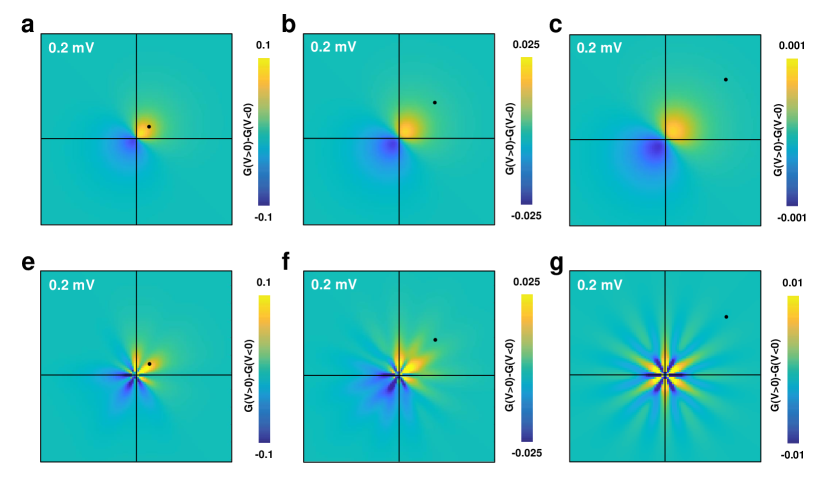
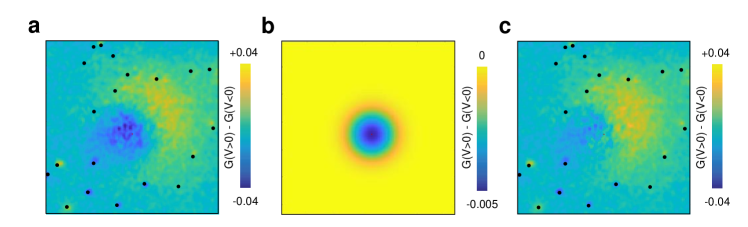
Figure S1: Vortex bound state asymmetry vs. distance of the magnetic impurity from the vortex center. The calculated difference of the normalized tunneling conductance between positive and negative bias voltages around the vortex center in a field of view of the same size as the ones shown in the main text. The center of the vortex is located at the origin (crossing point between the two black lines) and a single magnetic impurity is marked by a black dot. In a, e the impurity is located at 10 nm from the vortex core center and an angle of , in b, f at 30 nm and in c,g at 50 nm. Notice the color scale, given by the bars on the right of each figure. The radial asymmetry decreases by several orders of magnitude from a-c and from e-g.
If we neglect the rapid oscillations at the scale of , we can write the probability density difference between the electron-like () and the hole-like () states as
(18)
where
(19)
The difference of the normalized conductance between the positive and negative bias voltages is given by
(20)
where is the normal density of states at the Fermi energy, and
(21)
To obtain the results shown in the main text, we use 30 nm, = 9 nm-1, meV, 1 meV, 800 mK for both compounds. For 2H-NbSe2, we use , meVnm2 and meVnm2, whereas for 2H-NbSe1.8S0.2 we use , meVnm2 and meVnm2. meV-1nm-1 is used to fit the experimental data. Notice that the position of impurities is very different in both cases (Fig. 4 of the main text). The different values for can be associated to difference in the spatial dependence of the wavefunction, which becomes more important when the impurity is close to the vortex center. The actual values of are not relevant in the calculation of , as we show below.
To better understand the origin of our result, let us discuss a simple example taking just a single magnetic impurity and isotropic superconducting pairing, . In the weak perturbation limit, , the density of the perturbed state can be written as
(22)
where the coefficients are (up to a normalization factor close to one)
In the parameter regime we consider, and are monotonically decreasing functions with respect to and is small and positive of the order of . In the previous Eq. (24), we ignored the contribution from the non-magnetic potential in because it contains a small factor . The value of is positive for and negative for .
The denominator is in turn negative, so that Eq. (25) leads to positive and . So we can write
(26)
where . For the case of electron-like bands and within the same simplifying hypothesis one should change by . It is thus straightforward to conclude that the asymmetry in Eq.(26) would be inverted, i.e. would become .
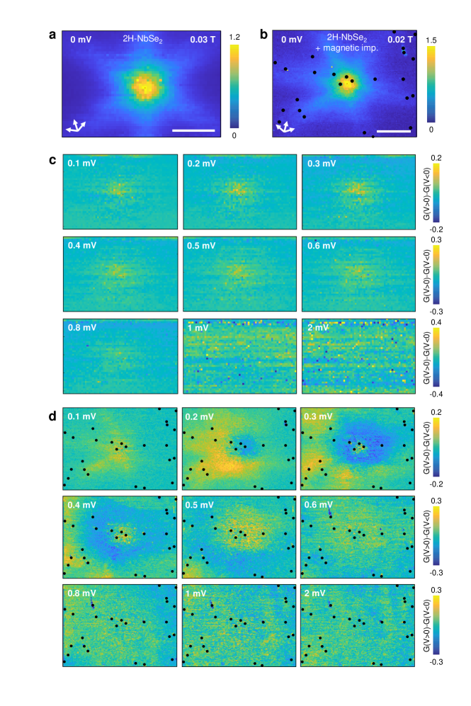
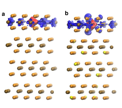
Figure S2: Electron hole symmetry of vortex cores with and without magnetic impurities.a shows a vortex imaged in a field of view without YSR impurities in 2H-NbSe2. We show of this vortex as a function of the bias voltage (indicated in each panel) in c. In b we show the same image as in Fig. 4d of the main text and in d we provide as a function of the bias voltage. White scale bars are 20 nm long. The atomic Se lattice directions are shown by three arrows.Figure S3: Relaxed atomic positions for 2H-NbSe2 and 2H-NbSe1.8S0.2 supercells. We show the atomic structure of the set of slabs used in the calculation, with Nb atoms in ocre, Se in orange and S in yellow, for supercell A a and supercell B b. Notice that the atomic positions are slightly modified due to the S substitution in b. The distribution of S in b is random. We also show a lateral view of the spin polarization due to the substituted Fe atom. We plot the spin isosurface corresponding to a spin imbalance in red (spin up) and blue (spin down).
We show the result of the calculation with a single magnetic impurity in Fig. S1a-c for and d-f for . We use meVnm2 and meVnm2. We see clearly the angular dependence shown in Eq. (26). The impurity induces an electron-hole asymmetry in the CdGM states when it is close to the center of the vortex. The electron-hole asymmetry close to the impurity is compensated by an asymmetry of opposite sign on the other side of the vortex. This breaks the axial symmetry of the vortex LDOS, with a mirror line that joins the vortex center with the impurity. When having many impurities, we add up the effect of each impurity to find the results discussed in the main text. Notice that, when the impurity is far from the vortex core Fig. S1c, the corresponding asymmetry decreases very rapidly. Therefore, the impurities closest to the vortex cores determine the axial symmetry breaking.
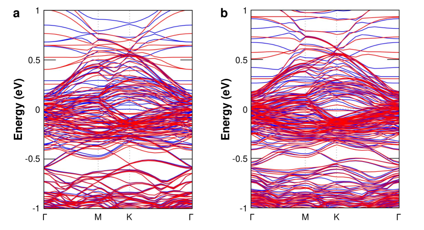
Figure S4: Spin resolved bandstructure of 2H-NbSe2 and of 2H-NbSe1.8S0.2. In a we show the calculated spin-polarized bandstructure for spin-up (blue) and spin-down (red) states and for 2H-NbSe2 with one Fe atom (supercell A). In b we show the same quantities for 2H-NbSe1.8S0.2 with one Fe atom (supercell B).
II S2. STM results with and without YSR impurities.
In Fig. S2 we compare the results obtained in a field of view without YSR impurities (Fig. S2a,c), with results with YSR impurities (Fig. S2b,d). We observe that the vortex is, for all , axially symmetric in absence of YSR impurities (Fig. S2c) and axially asymmetric (Fig. S2d) in presence of YSR impurities.
Notice the small electron-hole asymmetry in absence of YSR impurities (Fig. S2a,c), which we discuss below (Fig. S8).
III S3. Computational details of the spin-polarized electronic bandstructure calculations
Calculations.
We performed spin-polarized first principles calculations based on DFT with the generalized gradient approximation (GGA) of Perdew-Burke-ErnzerhofPhysRevLett.77.3865 for the exchange-correlation functional. The plane wave basis sets used projector augmented wave (PAW) pseudopotentialsPhysRevB.59.1758 and the electronic wave functions were expanded with well-converged kinetic energy cutoffs of 75 Ry and 500 Ry for the wavefunctions and charge density, respectively. Dispersion interactions to account for van der Waals interactions between the layers were considered by applying semi-empirical Grimme D2 correctionsdoi:10.1002/jcc.20495 .
Relaxed atomic arrangements.
To model the experimental system, we constructed slabs of 442 size formed by four layers (192 atoms each). The relaxed atomic positions are represented in Fig. S3, together with a lateral view of the spin isosurfaces discussed in the main text. All the structures were fully optimized without constraints until the forces on each atom were smaller than 103 Ry/au and the energy difference between two consecutive relaxation steps less than 104 Ry. The Brillouin zone was sampled by a centered 3 3 1 k-point Monkhorst-Pack PhysRevB.13.5188 mesh for structural optimization and 6 6 2 for the self-consistent field (SCF) calculations. We built two supercells. The supercell A is formed by a single Fe impurity substituting a Nb atom and 63 Nb and 128 Se atoms. The supercell B includes a 10% random substitution of Se by S atoms, resulting in 1 Fe, 63 Nb, 115 Se and 13 S atoms.
Magnetic interactions.
We inset a vacuum of 18 Å in between sets of cells, to avoid interaction between replica images as a result of periodic boundary conditions. In order to describe the strong correlation of electrons in Mott-Hubbard physics, we adopted a DFT+U approach, where U is the on-site Coulomb repulsion, using the simplified version proposed by Dudarev et alPhysRevB.57.1505 . The Hubbard U was estimated self-consistently using density functional perturbation theoryPhysRevB.98.085127 . The distance with the nearest periodic image is 1.4 nm, which is enough to discard any kind of interaction between the Fe ions. Generally, Nb atoms carry only small magnetic moments, that are oppositely oriented to the Fe moments. On the lateral edges of the supercell, however, we observe a polarization of Nb atoms which is small and might be influenced by the neighboring Fe sites. All calculations were carried out in the QuantumEspresso codeGiannozzi_2009 .
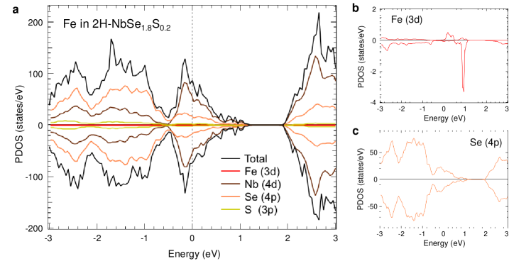
Figure S5: Partial densities of states of atomic species in 2H-NbSe1.8S0.2.a Spin-polarized partial densities of states integrated over the Brillouin zone for the orbitals marked in the figure for 2H-NbSe1.8S0.2 with one Fe atom (supercell B). The result for the Fe and Se orbitals is shown in b and c respectively.
Bandstructure.
In the Fig. S4a,b we plot the resulting spin resolved bandstructures of 2H-NbSe2 and of 2H-NbSe1.8S0.2 over the whole supercells. We see that the overall energy dependence of the density of states integrated over the whole Brillouin zone is very similar for both cases. The orbital dependent partial densities of states of orbitals that are close to the Fermi level (Se-3p, Nb-4d and S-3p), show nearly the same values for both spin orientations (Fig. S5), although there are slight but visible differences in the Nb and Se partial densities of states, corresponding to the spin polarization of the atoms located close to the Fe impurity. Of course, the result on the atomic Fe-3d orbitals show a clear spin polarization (inset of Fig. S5).
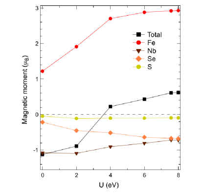
Magnetic moment.
In the Fig. S6 we show the dependence of the induced magnetic moment with U. We use a reduced system formed by a 4 4 slab of monolayer 2H-NbSe2 or of 2H-NbSe1.8S0.2 containing one Fe impurity that substitutes one Nb. We see that we reach convergence above about 7eV. We use U = 7.5681 eV in our calculations. However, it is also relevant to remark that the magnetic moment remains large already at relatively small values of U.
Figure S6: U parameter in calculations. Magnetic moment as a function of the U parameter for 2H-NbSe1.8S0.2 with one Fe atom (supercell B).
IV S4. STM measurements
To perform the STM measurements we prepared a plate like sample and glued it to our sample holder. We glued a piece of alumina on top of the sample and removed it at 4.2 K by pushing the piece with a beam. To this end, we used the movable sample holder described in Ref.Suderow2011 . We measured the freshly exposed surface in a cryogenic system with a base temperature of 800 mK. The design of the STM microscope is very similar to the one described in Ref.Suderow2011 ; Galvis2015 . We usually work with tunneling conductances of order of 0.1 S or below. We provide the tunneling conductance normalized to its value well above the gap edge, usually between 4 mV and 10 mV. Magnetic fields are applied perpendicular to the plate-like sample.
V S5. Crystal synthesis and characterization
Synthesis.
To synthesize samples of the 2H-NbSe2 and of 2H-NbSe1.8S0.2 we first mixed powders of Nb, Se (99.999% Se from Alfa-Aesar) and S (99.98% S from Sigma-Aldrich) in a stoichiometric ratio, and sealed these in an evacuated quartz ampoule. We heated from room temperature to 900 ∘C at 1.5 ∘C/min. Then, the temperature was kept constant for ten days and the furnace was switched off for cooling. We mixed 4 mmol of the previously synthesized material with iodine as transport agent (iodine concentration of 5 mg/cm3). We sealed the mixture in an evacuated quartz ampoule and placed it inside a three-zone furnace with the compound in the leftmost zone. The other two zones were heated up in 3 h from room temperature to 800 ∘C and kept at this temperature for two days. After that we established a gradient of 800 ∘C 750∘ 775 ∘C in the three-zone furnace. The temperatures were kept constant for 15 days and the furnace then cooled down naturally.
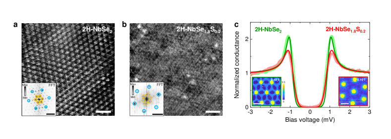
Figure S7: Topography, superconducting gap and vortex lattice in 2H-NbSe2 and 2H-NbSe1.8S0.2.a Topographic image of pure 2H-NbSe2. In the bottom left inset we show the Fourier transform of the topography. Atomic Bragg spots are marked with blue circles and CDW Bragg spots with orange circles. b Similar figure in a field of view of the same size in 2H-NbSe1.8S0.2. Scales bars on the bottom right are 3 nm long. c Normalized tunneling conductance vs bias voltage in 2H-NbSe2 (light green line, T=0.1 K) and in 2H-NbSe1.8S0.2 (orange line, T=0.8 K). These data are taken at zero field. The zero bias conductance maps showing the vortex lattice under magnetic fields are given in the lower left and right insets, with the color scale given in the lower left inset. Scale bars in the insets are 100 nm long.Figure S8: Axially symmetric electron-hole asymmetry.a Difference of the normalized tunneling conductance between positive and negative bias voltages, at 0.2 mV is shown as a color scale (bar on the right). b Slight electron-hole asymmetric background modelled using a simple gaussian function. c Map resulting from the subtraction of b from a. Black dots in a and c provide the positions of impurities.Figure S9: Bias voltage dependence of in 2H-NbSe1.8S0.2. We show in each panel for the bias voltages marked in each panel. The field of view is the same as in Fig. 4 of the main text. Black dots provide the position of magnetic impurities. Color scale is given by the bars on the right.
Characterization.
We obtained large single crystals, with lateral sizes in the order of several millimeters. The crystals were analyzed by powder X-ray diffraction and inductively coupled plasma (ICP) mass spectrometry. The experimental powder patterns were refined with the structure of pure 2H-NbSe2 (ICSD 51589) in both 2H-NbSe2 and of 2H-NbSe1.8S0.2. We obtained a variation in lattice constants with S doping compatible with literature (Å, Å in 2H-NbSe2 and , in 2H-NbSe1.8S0.2) doi:10.1002/zaac.200500233 ; PhysRevB.6.835 . Both and parameters of the hexagonal structure decrease by the same ratio, a result that remains when increasing the S concentrationSamuelToBePublished . To ascertain that S doping does not introduce defects other than substution, we have estimated the stacking fault density along the c-axis from the X-ray data. Being a van der Waals compound with little coupling between hexagonal 2H-NbSe2-xSx planes, we can expect most defects to occur along the c-axis. Following Ref. warren1990x , we can distinguish between deformation and growth faults, with respectively probabilities and . Deformation and growth faults can be estimated by analyzing reflections of the type H-K=3N1. We can then write for the full width at half maximum intensity of the powder scattering Bragg peaks with Miller indices HKL , for even L and for odd L, with the HKL spacing and warren1990x . We find that the amount of defects along the c-axis is around in both 2H-NbSe2 and 2H-NbSe1.8S0.2. From inductively coupled plasma (ICP) analysis, we observe 150 ppm of Fe. We do not detect further transition metal impurities within the detection limits of ICP.
The superconducting density of states at zero field of 2H-NbSe1.8S0.2 shows a smooth distribution of gap valuesFente2016 . It is useful to compare the effect of S substitution with the application of pressure in 2H-NbSe2PhysRevLett.95.117006 ; PhysRevResearch.2.043392 . Pressure increases Tc up to 8.5 K at 10GPa, and then Tc is slightly reduced to 7.5 K at 20 GPa. S substitution by contrast decreases TcCho2018 . As shown in Ref. Fente2016 , the charge density wave (CDW) of 2H-NbSe2, becomes strongly affected by S substitution in 2H-NbSe1.8S0.2. In Fig. S7a,b we compare topographic STM images of 2H-NbSe2 with 2H-NbSe1.8S0.2. 2H-NbSe2 shows CDW order with periodic modulations three times the in-plane lattice constant. In 2H-NbSe1.8S0.2 we also find CDW order at the same wavevector than for . However, the intensity of the CDW modulation strongly varies with position, producing a disordered CDW pattern. Thus, the S substitution in 2H-NbSe1.8S0.2 leads to a superconductor which is very similar to 2H-NbSe2, but in-plane isotropic. The mean free path estimated from the residual resistivity is of about 20 nm in 2H-NbSe1.8S0.2, significantly below 120 nm in 2H-NbSe2. However, CdGM bound states are well identified in the LDOSFente2016 .
Superconducting gap and vortex lattice.
In Fig. S7c we show the superconducting gap and vortex lattice in pure 2H-NbSe2 and in 2H-NbSe1.8S0.2. The results in 2H-NbSe2 have been obtained repeatedly in the past (see e.g. Hess1989 ; Hess1990 ; Guillamon2008c ) and correspond to a superconductor having different values of the gap over the Fermi surface. This is somewhat different in 2H-NbSe1.8S0.2, which shows a more homogeneous gap distribution. The vortex lattice of 2H-NbSe1.8S0.2 loses the sixfold star shape characteristic of 2H-NbSe2 and vortices have instead a round shape (bottom insets of Fig. S7c)Fente2016 .
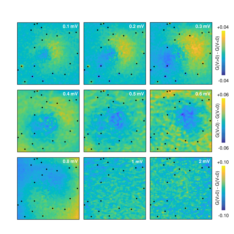
VI S6. Complete bias voltage dependence in 2H-NbSe1.8S0.2.
We have subtracted a radially symmetric signal to to obtain the images shown in the main text for 2H-NbSe1.8S0.2. As we show in Fig. S8, the radially symmetric electron hole anisotropy in is very small, of less than 10% of . For completeness, we provide the results for all bias voltages in 2H-NbSe1.8S0.2 in Fig. S9. We observe that for bias voltages above 0.3 mV, the in-plane asymmetry is washed out and there is no signal for bias voltages above the superconducting gap.
VII S7. Magnetic susceptibility measurements and large size conductance maps at zero field and under magnetic fields in the normal phase
Magnetic susceptibility of the bulk.
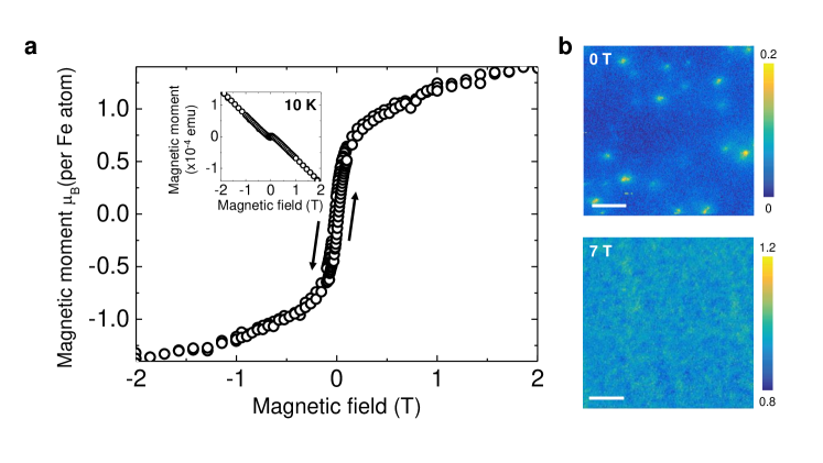
We have performed susceptibility measurements in the same samples measured by STM using a Quantum Design PPMS system, with the magnetic field applied perpendicular to the plate like sample. Inside the superconducting phase, the signal is dominated by the superconducting diamagnetic response. Above we observe a diamagnetic background and a small signal which is ferromagnetic like (Fig. S10a). We can extract this small ferromagnetic like component from the background and compare its size with the expected Fe moment, taking a Fe concentration of 150 ppm. It is quite remarkable that, although being clearly a very rough approximation which might be strongly influence by clustering at edges or on large defects induced during growth, we obtain a saturation magnetization with a moment of about a Bohr magneton per Fe ion, compatible with the value found in the theoretical calculations (Fig. S6). Previous measurements with much larger (30%) Fe concentration report values up to five Bohr magnetonsVOORHOEVEVANDENBERG1971167 , which are compatible with a Fe4+ valence. The reduced magnetic moment obtained here points to a reduction of the Fe valence, which might be chemically compensated by Se vacancies. More recently, the substitional exchange of Fe atoms in transition metal dichalcogenide MoS2 has been studied in detail, observing directly the exchange of transition metal atoms and finding similarly spin-polarized electronic bandstructure in small cells of transition metal dichalcogenide layers containing one Fe atomFu2020 .
Maps at zero field and in the normal phase.
We provide a large size zero bias conductance map at zero field (Fig. S10b) and under magnetic fields above the critical field of 2H-NbSe1.8S0.2 (Fig. S10c). These show that impurities are generally well separated. Furthermore, impurities do not influence the zero bias density of states of the normal phase above the critical field.
Figure S10: Macroscopic magnetic susceptibility of Fe impurities in 2H-NbSe1.8S0.2.a We show as circles the magnetic moment as a function of the magnetic field at 10 K. To obtain this curve, we have subtracted a diamagnetic background from the magnetization as a function of the magnetic field (shown in the inset) and divided by the estimated concentration of Fe atoms in the sample, taking the 150 ppm value determined from inductively coupled plasma analysis. Arrows show the direction of the field sweep. b Tunneling conductance at zero bias normalized to the tunneling conductance at large bias at zero field (top panel) and at 7 T (bottom panel). Color scale (bars at the right) show the normalized conductance values.
References
(1)
Johannes, M. D., Mazin, I. I. &
Howells, C. A.
Fermi-surface nesting and the origin of the
charge-density wave in NbSe2.
Phys. Rev. B73,
205102 (2006).
(2)
Fletcher, J. D. et al.Penetration depth study of superconducting gap
structure of .
Phys. Rev. Lett.98, 057003
(2007).
(3)
Majumdar, A. et al.Interplay of charge density wave and multiband
superconductivity in layered quasi-two-dimensional materials: The case of
and
.
Phys. Rev. Materials4, 084005 (2020).
(4)
Caroli, C., deGennes, P. G. &
Matricon, J.
Bound fermion states on a vortex line in a type
II superconductor.
Physics Letters9, 307 – 309
(1964).
(5)
Bardeen, J., Kümmel, R.,
Jacobs, A. E. & Tewordt, L.
Structure of vortex lines in pure superconductors.
Phys. Rev.187,
556–569 (1969).
(6)
Clinton, W. L.
Approximate solutions for the Bogoliubov de Gennes
equations: Superconductor normal metal superconductor junctions and the
vortex problem.
Phys. Rev. B46,
5742–5745 (1992).
(7)
Gygi, F. & Schlüter, M.
Self-consistent electronic structure of a vortex line
in a type-II superconductor.
Phys. Rev. B43,
7609–7621 (1991).
(8)
Fischer, Ø., Kugler, M.,
Maggio-Aprile, I., Berthod, C. &
Renner, C.
Scanning tunneling spectroscopy of high-temperature
superconductors.
Rev. Mod. Phys.79, 353–419
(2007).
(9)
Hayashi, N., Isoshima, T.,
Ichioka, M. & Machida, K.
Low-lying quasiparticle excitations around a vortex
core in quantum limit.
Phys. Rev. Lett.80, 2921–2924
(1998).
(10)
Rainer, D., Sauls, J. A. &
Waxman, D.
Current carried by bound states of a superconducting
vortex.
Phys. Rev. B54,
10094–10106 (1996).
(11)
Bespalov, A. A. & Plastovets, V. D.
Large spectral gap and impurity-induced states in a
two-dimensional abrikosov vortex.
Phys. Rev. B103, 024510
(2021).
(12)
Perdew, J. P., Burke, K. &
Ernzerhof, M.
Generalized gradient approximation made simple.
Phys. Rev. Lett.77, 3865–3868
(1996).
(13)
Kresse, G. & Joubert, D.
From ultrasoft pseudopotentials to the projector
augmented-wave method.
Phys. Rev. B59,
1758–1775 (1999).
(14)
Grimme, S.
Semiempirical gga-type density functional constructed
with a long-range dispersion correction.
Journal of Computational Chemistry27, 1787–1799
(2006).
(15)
Monkhorst, H. J. & Pack, J. D.
Special points for brillouin-zone integrations.
Phys. Rev. B13,
5188–5192 (1976).
(16)
Dudarev, S. L., Botton, G. A.,
Savrasov, S. Y., Humphreys, C. J. &
Sutton, A. P.
Electron-energy-loss spectra and the structural
stability of nickel oxide: An lsda+u study.
Phys. Rev. B57,
1505–1509 (1998).
(17)
Timrov, I., Marzari, N. &
Cococcioni, M.
Hubbard parameters from density-functional
perturbation theory.
Phys. Rev. B98,
085127 (2018).
(18)
Giannozzi, P. et al.QUANTUM ESPRESSO: a modular and open-source
software project for quantum simulations of materials.
Journal of Physics: Condensed Matter21, 395502
(2009).
(19)
Suderow, H., Guillamón, I. &
Vieira, S.
Compact very low temperature scanning tunneling
microscope with mechanically driven horizontal linear positioning stage.
Review of Scientific Instruments82 (2011).
(20)
Galvis, J. A. et al.Three axis vector magnet set-up for cryogenic
scanning probe microscopy.
Review of Scientific Instruments86 (2015).
(21)
Hotje, U. & Binnewies, M.
Chemischer transport fester lösungen. 23 [1] der
chemische transport von mischphasen im system mos2/mose2, mos2/nbs2,
mose2/nbse2 und nbs2/nbse2.
Zeitschrift für anorganische und allgemeine
Chemie631, 2467–2474
(2005).
(22)
Jones, R. E., Shanks, H. R.,
Finnemore, D. K. & Morosin, B.
Pressure effect on superconducting
nb and nb.
Phys. Rev. B6,
835–838 (1972).
(23)
S. Mañas et al., in preparation.
(24)
Warren, B. E.
X-ray Diffraction
(Courier Corporation, 1990).
(25)
Fente, A. et al.Field dependence of the vortex core size probed by
scanning tunneling microscopy.
Phys. Rev. B94,
014517 (2016).
(26)
Suderow, H., Tissen, V. G.,
Brison, J. P., Martínez, J. L. &
Vieira, S.
Pressure induced effects on the fermi surface of
superconducting
.
Phys. Rev. Lett.95, 117006
(2005).
(27)
Moulding, O., Osmond, I.,
Flicker, F., Muramatsu, T. &
Friedemann, S.
Absence of superconducting dome at the
charge-density-wave quantum phase transition in
.
Phys. Rev. Research2, 043392 (2020).
(28)
Cho, K. et al.Using controlled disorder to probe the interplay
between charge order and superconductivity in nbse2.
Nature Communications9, 2796 (2018).
(29)
Hess, H. F., Robinson, R. B.,
Dynes, R. C., Valles, J. M. &
Waszczak, J. V.
Scanning-tunneling-microscope observation of the
Abrikosov flux lattice and the density of states near and inside a
fluxoid.
Phys. Rev. Lett.62, 214–216
(1989).
(30)
Hess, H. F., Robinson, R. B. &
Waszczak, J. V.
Vortex-core structure observed with a scanning
tunneling microscope.
Phys. Rev. Lett.64, 2711–2714
(1990).
(31)
Guillamon, I., Suderow, H.,
Guinea, F. & Vieira, S.
Intrinsic atomic-scale modulations of the
superconducting gap of 2H-NbSe2.
Phys. Rev. B77,
134505 (2008).
(32)
Voorhoeve-van Den Berg, J. & Sherwood,
R.
Low-temperature magnetic susceptibilities of nbse2
containing the first-row transition metals.
Journal of Physics and Chemistry of Solids32, 167 – 173
(1971).
(33)
Fu, S. et al.Enabling room temperature ferromagnetism in monolayer
mos2 via in situ iron-doping.
Nature Communications11, 2034 (2020).