Laser soliton microcombs on silicon
Silicon photonics enables wafer-scale integration of optical functionalities on chip. A silicon-based laser frequency combs could significantly expand the applications of silicon photonics, by providing integrated sources of mutually coherent laser lines for terabit-per-second transceivers, parallel coherent LiDAR, or photonics-assisted signal processing. Here, we report on heterogeneously integrated laser soliton microcombs combining both InP/Si semiconductor lasers and ultralow-loss Si3N4 microresonators on monolithic Si substrate. Thousands of devices are produced from a single wafer using standard CMOS techniques. Using on-chip electrical control of the microcomb-laser relative optical phase, these devices can output single-soliton microcombs with 100 GHz repetition rate. Our approach paves the way for large-volume, low-cost manufacturing of chip-based frequency combs for next-generation high-capacity transceivers, datacenters, space and mobile platforms.
Optical frequency combs (OFC) Udem et al. (2002); Cundiff and Ye (2003) have revolutionized timing, spectroscopy and metrologyFortier and Baumann (2019); Diddams et al. (2020). Historically, OFCs have been made using femtosecond mode-locked lasers with supercontinuum generation for octave-spanning spectra, required for self-referencing. Discovered a decade ago Del’Haye et al. (2007), OFCs can also be generated in driven Kerr-nonlinear optical microresonators. These types of OFCs are commonly referred to as "microcombs". Microcombs can be operated in regimes where they form coherent, temporal, dissipative structures Lugiato and Lefever (1987); Akhmediev and Karlsson (1995), i.e. bright dissipative Kerr solitons (DKS) Herr et al. (2013). DKS have unlocked the full potential of microcombs by providing coherent, broadband OFCs with repetition rates in the terahertz to microwave domains, and have been successfully employed in many system-level applications such as RF photonicsTorres-Company and Weiner (2014); Wu et al. (2018), coherent communication Marin-Palomo et al. (2017); Corcoran et al. (2020), astronomical spectrometer calibration Suh et al. (2019); Obrzud et al. (2019), massively parallel coherent LiDAR Riemensberger et al. (2020), optical frequency synthesizers Spencer et al. (2018) and photonic neromorphic computing Feldmann et al. (2021); Xu et al. (2021). On a fundamental level, DKS microcombs have allowed explorations of a plethora of novel nonlinear dynamics and phenomena Xue et al. (2015); Yang et al. (2017).
In parallel, there has been substantial progress in photonic integrated platforms Kovach et al. (2020) for microcomb generation, which to date include Si3N4Moss et al. (2013); Xuan et al. (2016); Ji et al. (2017); Liu et al. (2020a); Ye et al. (2019), AlNJung et al. (2014); Liu et al. (2020b), LiNbO3He et al. (2019a); Wang et al. (2019); Gong et al. (2020), AlGaAsPu et al. (2016); Chang et al. (2020); Moille et al. (2020), GaPWilson et al. (2020), and SiCLukin et al. (2020). Among them, the leading platform is Si3N4, which has already been used widely in CMOS microelectronics as diffusion barriers and etch masks. In addition to its native properties such as the absence of two-photon absorption, high Kerr nonlinearity, and weak Raman and Brillouin gains Gyger et al. (2020), recent advances in fabrication of nonlinear Si3N4 photonic integrated circuits (PIC) have enabled optical propagation losses below 1 dB/m Ji et al. (2017); Liu et al. (2020a). These ultralow losses have significantly reduced the soliton formation threshold power to the levels that integrated lasers can provide Huang et al. (2019a); McKinzie et al. (2021), and have yielded soliton repetition rates in the microwave X-band Liu et al. (2020c). In combination with negligible thermal effects and almost purely Kerr-dominated frequency-dependent response Liu et al. (2020a), reliable soliton generation can be attained without complex or fast laser tuning. Additionally, laser self-injection locking Liang et al. (2015a); Pavlov et al. (2018) and hybrid integration of soliton microcombs with RSOAs Stern et al. (2018) or DFB lasers Shen et al. (2020) allow for current-initiated and electrically controlled modules with low electrical power Stern et al. (2018); Raja et al. (2019); Shen et al. (2020); Jin et al. (2021).
A long-standing goal is to monolithically integrate lasers and high- nonlinear microresonators onto a common silicon wafer. Heterogeneously integrated silicon photonics Komljenovic et al. (2016); Liang and Bowers ; Zhang et al. (2019a) offers a compelling solution using low-cost, industry-standard silicon substrates, aided by mature CMOS-compatible fabrication facilities. High-performance, large-scale heterogeneous PICs with complete functionalities, including lasers Fang et al. (2006); Liang and Bowers (2010); Xiang et al. (2020), modulators Xu et al. (2005); Reed et al. (2010); Hiraki et al. (2017), and photodetectors Xie et al. (2016); Michel et al. (2010), are disrupting optical interconnect technology and other applications Roelkens et al. (2010); Jones et al. (2019); Sun et al. (2013). The material-by-design nature enabled by heterogeneous integration offers best-in-class performance. However, heterogeneous integration of high-power, narrow-linewidth, semiconductor lasers with high- Si3N4 microresonators has not been demonstrated yet, because multiple material platforms (Si, Si3N4, and III-V) with significantly different optical properties have to be deployed and combined. Here we overcome these challenges and present the first demonstration of heterogeneously integrated laser soliton microcombs. This is achieved using ultralow-loss Si3N4 PICs based on the photonic Damascene fabrication process in conjunction with direct SOI wafer bonding and heterogeneous III-V integration. The result is a wafer-scale fabrication process that produces thousands of devices from one silicon wafer. Each device allows electrical initiation and control of soliton microcombs. Our technology demonstrates the viability of large-volume, low-cost manufacturing of chip-based OFCs, and allows incorporation of soliton microcombs as new building block into existing complex silicon photonics systems, and in applications requiring reliable performance, small footprint, low cost and low power consumption, such as space or mobile platforms.
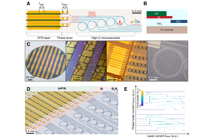
Device schematic. As shown in Fig. 1A, a chip-scale laser frequency comb consists of three main parts: a distributed feedback (DFB) laser, a thermo-optic phase tuner, and a high- nonlinear microresonator, by leveraging multilayer heterogeneous integrationXiang et al. (2020) (Fig. 1B). Figure 1C shows the photographs of the complete wafer (before dicing into chips), multiple dies, single-die-level devices, and an optical microscope image of a Si3N4 microring resonator interfaced with Si layer. As illustrated in Fig. 1D, the DFB lasers, phase tuners, and nonlinear microresonators are built on indium phosphide/silicon (InP/Si), silicon (Si), and Si3N4 layers, respectively. This vertical, multilayer structure is realized through sequential wafer bonding of a silicon-on-insulator (SOI) wafer and an InP multiple-quantum-well (InP MQW) epi wafer to a pre-patterned Si3N4 substrate that is fabricated using the photonic Damascene process Liu et al. (2020a); Xiang et al. (2020). Deep ultra-violet (DUV) stepper lithography is used to ensure pattern alignment on each individual layer with an accuracy better than 100 nm. Here we directly apply heterogeneous integration on 100-mm-diameter Si substrates and process the entire substrate on the wafer scale. Our process could be further scaled up with larger wafer substrates such that it is compatible with standard CMOS foundry production lines Jones et al. (2019).
The DFB laser is a high-power, single longitudinal-mode pump source with an excellent side mode suppression ratio (SMSR) such that the laser wavelength can be tuned to a microring resonanceColdren et al. (2012). The laser has a 1.8-mm-long InP/Si gain section, and the grating is etched on both sides of the shallow-etched Si waveguide rib with a 170 nm gap separation to the Si waveguide core. The fully etched grating provides the optical resonant feedback for the pump laser and determines the lasing wavelength by its pitch (). Here nm and nm. A quarter wavelength shift section is included at the grating length center to supply non-degenerate phase conditions favoring single longitudinal mode lasing.
The single-wavelength laser output passes through a thermo-optic resistive heater (for optical phase control), and couples into a high- Si3N4 microring resonator where nonlinear four-wave mixing processes generate Kerr microcombsKippenberg et al. (2004); Del’Haye et al. (2007). The Si3N4 microresonator exhibits anomalous group velocity dispersion (GVD) in the telecommunication C band and have a free-spectral range (FSR) of 100 GHz. The laser directly pumps the microresonator without an intermediate optical isolator, and the entire device is operated via laser control and phase control. Laser self-injection locking Kondratiev et al. (2017); Liang et al. (2015b, a); Raja et al. (2019); Shen et al. (2020); Jin et al. (2021) leverages the narrow-band optical feedback at desired phase relations from a high- microresonator to stabilize the pump laser and pulls the laser frequency towards the microring resonance. In this scenario, soliton microcombs can form when optimum laser-resonator frequency detuning is reached. Only the laser and phase tuner currents are electronically controlled, and no sophisticated external electronics feedback controls are required. The DFB laser wavelength increases with increasing laser current, as the grating index increases due to injected electrical power heating. As a result, certain gain currents triggers comb generation if the laser wavelength coincides with a microresonator resonance. The comb generation region resides where the laser is red-detuned to the resonance and the phase of the back-scattered light from the microresonator to the laser fulfills certain phase relations (Fig. 1E, see Supplementary Information for details). Note that the back-scattered light originates from Rayleigh scattering inside the microresonator due to surface roughness and bulk inhomogeneity.
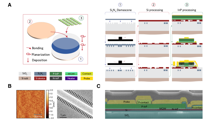
Fabrication process flow. Figure 2A presents the wafer-scale fabrication process flow. It starts with the photonic Damascene process Liu et al. (2020a) to fabricate the Si3N4 PIC on a Si substrate with 4-µm-thick thermal wet SiO2. The Si3N4 PIC is exposed with DUV stepper lithography and transferred to the SiO2 substrate to form the waveguide preform. Stoichiometric Si3N4 is deposited on the patterned SiO2 preform using low-pressure chemical vapor deposition (LPCVD), filling the trenches and forming waveguide cores. Chemical-mechanical polishing (CMP) is used to remove excess Si3N4 and planarize the wafer front surface, followed by spacer SiO2 deposition of 300 nm thickness on the Si3N4 substrate. The entire substrate is further annealed at 1200∘C to drive out the residual hydrogen content in the Si3N4 and SiO2 films, and to densify the spacer SiO2.
A second CMP is performed to create a flat and smooth wafer surface. As shown in Fig. 2B left, the measured RMS roughness of the wafer surface using atomic-force microscopy (AFM) is 0.27 nm, enabling direct substrate bonding with an SOI wafer. After removing the Si substrate of the bonded SOI wafer, the Si device layer is processed to create waveguide structures with different etch depths, including shallow-etched Si waveguides for the lasers and phase tuners, fully-etched hole structures for gratings (cf. Fig. 2B right), and thin-thickness Si tapers for mode conversion between the Si waveguide and underlying Si3N4 waveguideXiang et al. (2020). InP MQW epi is then bonded to the patterned Si device surface at the active regions. The InP process starts with InP substrate removal. InP mesa etches including P-type InP, AlInGaAs MQW, and N-type InP etches are performed using selective dry etching and wet etching. The P- and N-type contact metals are deposited on the P-InGaAs layer and N-InP layer respectively. The excess Si on top of the Si3N4 microresonators is removed before laser passivation using hydrogen-free deuterated SiO2 depositionJin et al. (2020). Vias are then etched through it for laser electrical contact. Proton implantation is performed on the laser mesa structure to reduce electrical current leakage. Heater and probe metals are deposited at the end of the full process. Finally, the entire wafer is diced into dozens of dies/chips to facilitate testing. Each chip contains tens of devices for soliton generation. Figure 2C shows the scanning electron microscopic (SEM) images of the device cross-section, which is false-colored to illustrate the multilayer structure.
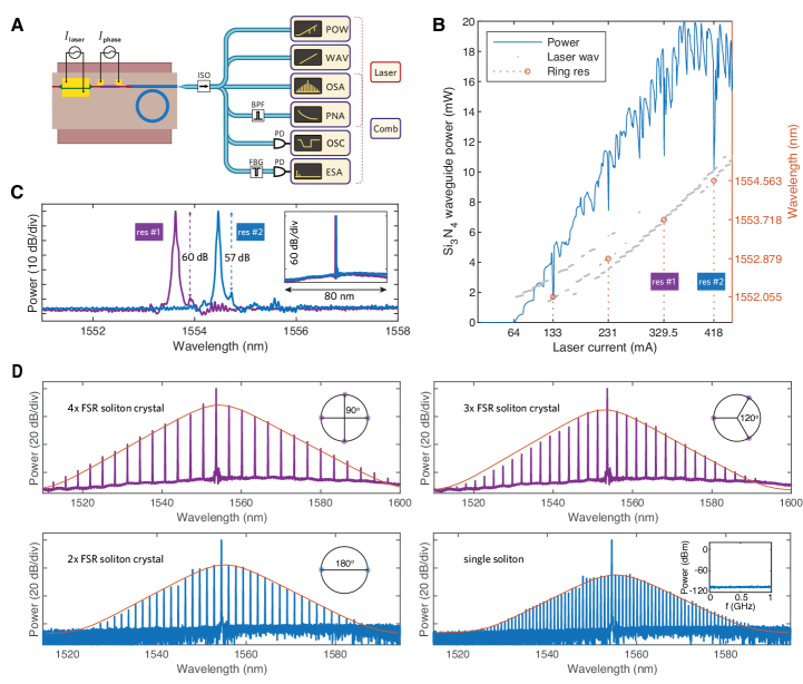
Soliton generation. The experimental setup to characterize the final chip devices is shown in Fig. 3A. We first characterize the laser performance. Figure 3B shows the measured light-current curves (solid blue curve), i.e. the laser output power versus stepped laser injection current of 0.5 mA, fixed phase tuner current of 7 mA, and 20∘C stage temperature. The measured laser threshold current is 64 mA. The laser power is out-coupled from the Si3N4 waveguide inverse-taper to a lensed fiber. The maximum power in the output fiber is measured as 8 mW, and the corresponding on-chip power in the Si3N4 waveguide is approximately 20 mW. The measured laser center wavelength using a wavelength meter is shown in Fig. 3B (dashed grey curve). Several dips on the optical power are observed at laser currents of 133, 231, 329.5, and 418 mA, where the laser wavelength coincides with microresonator resonances. These dips also verify the microresonator FSR of 100 GHz. Note that a high-reflection (HR) coating is applied on the other side of the DFB laser to boost the laser output power. Future devices can avoid using this coating to yield mode-hop-free DFB lasers and linearized laser wavelength dependence on the laser current. The DFB laser has high SMSR at resonance #1 and #2, where high output powers are also obtained that are advantageous for comb generation. Figure 3C shows the single-longitudinal-mode laser spectra at the two resonance wavelengths, with 60 and 57 dB SMSR, respectively.
Soliton microcomb is generated by tuning the laser frequency to the microresonator resonance via biasing the laser current, together with tuning the current of the phase tuner to control the relative forward/backward phase relations. As no optical isolator is used between the laser and the Si3N4 microresonator, laser self-injection lockingKondratiev et al. (2017); Liang et al. (2015b); Shen et al. (2020) occurs when the laser frequency coincides with a microresonator resonance. More information of the phase dependence on comb generation is revealed by simulating the nonlinear self-injection locking processVoloshin et al. (2021) and is discussed in the Supplementary Information. The calculated Kerr parametric oscillation threshold Kippenberg et al. (2004) for Si3N4 microresonators of (see Supplementary information for measurement) and 100 GHz FSR, is estimated to be around 3 mW. With around 329 mA laser current, the estimated on-chip laser power to pump the Si3N4 microresonator exceeds 16 mW. As shown in Fig. 3D, perfect soliton crystal statesKarpov et al. (2019) are observed by fine-tuning the laser frequency. We also observe soliton crystal states with decreasing crystallization orders when increasing the laser current (red-detuning). Further increasing the laser power to around 418 mA current, a two-soliton crystal state with 200 GHz repetition rate and a single-soliton state with 100 GHz repetition rate is generated. The coherent soliton nature is revealed by photodetection of the amplitude noise of the comb lines beat signal. Once generated, the soliton states can be stable for hours in standard lab environments without any external feedback control. This stability benefits from the monolithic nature of the chip device and the laser-microresonator coupling through laser self-injection locking.
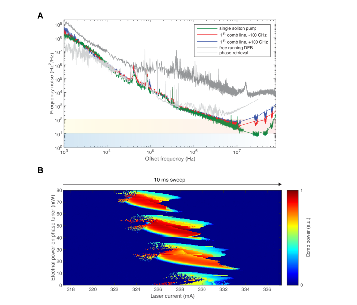
Self-injection locking and phase noise reduction. To further characterize the laser self-injection locking, we measured the frequency noise spectra of the pump line and comb line in the single soliton state and laser free-running state, as shown in Fig. 4A. Leveraging a high- external cavity, self-injection locking exhibits frequency noise reduction, i.e. laser linewidth narrowing Liang et al. (2015b). The fundamental linewidth of the free-running DFB laser is around 60 kHz, and is reduced to about 25 Hz in the self-injection-locked single soliton state. A 10-dB noise reduction is observed at 1 kHz Fourier offset frequency and is further increased to more than 30 dB above 300 kHz offset frequency. It has been revealed recently that the frequency noise of a self-injection-locked laser to a high- Si3N4 microresonator can be dominantly limited by the thermo-refractive noise of the microresonator Huang et al. (2019b); Jin et al. (2021). Therefore, further noise reduction can be realized by using microresonators of larger sizes (i.e. smaller FSR) or engineered material properties with lower thermo-optic transduction. Though the free-running linewidth of the DFB laser is broad, due to the linewidth narrowing provided by self-injection locking, the laser is still able to directly generate soliton states, surpassing its intrinsic limitation of spectral impurity. Additionally, the coherence of the injection-locked pump line is transferred to other comb lines. For example, the first neighboring comb lines, 100 GHz apart from the pump, have a fundamental linewidth around 200 to 300 Hz, and their frequency noise below 10 MHz offset frequency directly inherits that of the self-injection-locked pump. The self-injection locking scheme thus enables multi-wavelength, narrow-linewidth laser sources. Our device represents the first demonstration of a self-injection-locked, narrow-linewidth laser on Si.
Different from the conventional pumping scheme with an optical isolator, the comb generation in the self-injection locking scheme relies critically on the phase relation between the forward signal (i.e. the laser emission to the microresonator) and backward signal (i.e. the back-scattered light from the microresonator to the laser). In this case, comb generation is only allowed when the optical phase difference is within a certain optimized range. In previous works using hybrid integrated devices, controlling the phase difference is realized by varying the gap distance between the laser chip and Si3N4 chip, which however also causes power coupling efficiency fluctuation between these two chips. In our monolithic device, this optical phase difference can be directly controlled by varying the current to the phase tuner. We experimentally studied the comb formation with laser current sweep under different currents on the phase tuner. In order to exclude the interference from the mode-hop phenomenon when monitoring the power of the new frequency components, we sweep the laser current across the resonance #1 shown in Fig. 3B. Results shown in Fig. 4B unveils that the comb generation is only permitted with certain phase conditions. More study shown in the Supplementary Information indicates that the back-scattered signal needs to be in phase with the forward signal. Additionally, the phase altering effect is periodic and deterministic with the applied electrical power on the phase tuner. Thus the allowed comb generation area depends mainly on the pump power and the intensity of the back-scattered light (see Supplementary Information).
In summary, we have presented the first heterogeneously integrated laser soliton microcomb on silicon. Thousands of devices are manufactured from a full wafer-scale fabrication process using standard CMOS techniques such as DUV stepper lithography, CMP, wafer bonding, etc. We have successfully demonstrated single soliton formation with 100 GHz repetition rate, and characterized laser performance with self-injection locking. More functions could be added based on our current technology. For example, active, high-speed tuning of the Si3N4 microresonators (thus the injection-locked laser frequency) can be realized using piezoelectric actuators Jin et al. (2018); Liu et al. (2020d). Meanwhile, full integration with other nonlinear photonics platforms such as (Al)GaAs Chang et al. (2020, 2019) and LiNbO3 Zhang et al. (2019b); Boes et al. (2018); He et al. (2019b) could provide nonlinearity that can be used for electro-optic modulation and second harmonic generation. The laser gain material can also be modified to utilize quantum-dots Liu et al. (2015) or extended to different wavelength ranges from the visible to mid-infrared, significantly complementing existing integrated nonlinear photonic systems. Though demonstrated here on 100-mm-diameter Si substrates, our process could be upgraded to 200- or 300-mm-diameter substrates using modified CMOS foundry pilot lines. Our work paves the way for large-volume, low-cost manufacturing of electrically controlled, chip-based frequency comb modules for future applications in data-centers, space and mobile platforms.
Acknowledgments: We thank Mario Dumont and Jijun He for their help in the device characterization. This work is supported by the Defense Advanced Research Projects Agency (DARPA) under DODOS (HR0011-15-C-055) programmes of the Microsystems Technology Office (MTO).
Author contribution: C.X., L.C., J.L., T.J.K. and J.E.B. conceived the idea and initiated the collaboration. C.X., J.L. and L.C. designed the wafer layout and process flow. J.L. and R.N.W. fabricated the Si3N4 substrate. C.X. and J.P. fabricated the heterogeneous InP/Si lasers and Si circuits with the assistance from W.X., and Z.Z. C.X., J.G., and J.L. tested the final chips. C.X. and J.G. performed the laser soliton experiments with the assistance from J.R.. W.W. performed the numerical simulations of self-injection locking. J.S. took the FIB-SEM image. All authors discussed the data. C.X., J.L. and W.W. wrote the manuscript, with input from others. T.J.K. and J.E.B supervised the project.
Data Availability Statement: All data generated or analysed during this study are available within the paper and its Supplementary Information. Further source data will be made available on reasonable request.
References
- Udem et al. (2002) T. Udem, R. Holzwarth, and T. W. Hänsch, Nature 416, 233 (2002).
- Cundiff and Ye (2003) S. T. Cundiff and J. Ye, Rev. Mod. Phys. 75, 325 (2003).
- Fortier and Baumann (2019) T. Fortier and E. Baumann, Communications Physics 2, 153 (2019).
- Diddams et al. (2020) S. A. Diddams, K. Vahala, and T. Udem, Science 369 (2020), 10.1126/science.aay3676.
- Del’Haye et al. (2007) P. Del’Haye, A. Schliesser, O. Arcizet, T. Wilken, R. Holzwarth, and T. J. Kippenberg, Nature 450, 1214 (2007).
- Lugiato and Lefever (1987) L. A. Lugiato and R. Lefever, Phys. Rev. Lett. 58, 2209 (1987).
- Akhmediev and Karlsson (1995) N. Akhmediev and M. Karlsson, Phys. Rev. A 51, 2602 (1995).
- Herr et al. (2013) T. Herr, V. Brasch, J. D. Jost, C. Y. Wang, N. M. Kondratiev, M. L. Gorodetsky, and T. J. Kippenberg, Nature Photonics 8, 145 (2013).
- Torres-Company and Weiner (2014) V. Torres-Company and A. M. Weiner, Laser & Photonics Reviews 8, 368 (2014).
- Wu et al. (2018) J. Wu, X. Xu, T. G. Nguyen, S. T. Chu, B. E. Little, R. Morandotti, A. Mitchell, and D. J. Moss, IEEE Journal of Selected Topics in Quantum Electronics 24, 1 (2018).
- Marin-Palomo et al. (2017) P. Marin-Palomo, J. N. Kemal, M. Karpov, A. Kordts, J. Pfeifle, M. H. P. Pfeiffer, P. Trocha, S. Wolf, V. Brasch, M. H. Anderson, R. Rosenberger, K. Vijayan, W. Freude, T. J. Kippenberg, and C. Koos, Nature 546, 274 (2017).
- Corcoran et al. (2020) B. Corcoran, M. Tan, X. Xu, A. Boes, J. Wu, T. G. Nguyen, S. T. Chu, B. E. Little, R. Morandotti, A. Mitchell, and D. J. Moss, Nature Communications 11, 2568 (2020).
- Suh et al. (2019) M.-G. Suh, X. Yi, Y.-H. Lai, S. Leifer, I. S. Grudinin, G. Vasisht, E. C. Martin, M. P. Fitzgerald, G. Doppmann, J. Wang, D. Mawet, S. B. Papp, S. A. Diddams, C. Beichman, and K. Vahala, Nature Photonics 13, 25 (2019).
- Obrzud et al. (2019) E. Obrzud, M. Rainer, A. Harutyunyan, M. H. Anderson, J. Liu, M. Geiselmann, B. Chazelas, S. Kundermann, S. Lecomte, M. Cecconi, A. Ghedina, E. Molinari, F. Pepe, F. Wildi, F. Bouchy, T. J. Kippenberg, and T. Herr, Nature Photonics 13, 31 (2019).
- Riemensberger et al. (2020) J. Riemensberger, A. Lukashchuk, M. Karpov, W. Weng, E. Lucas, J. Liu, and T. J. Kippenberg, Nature 581, 164 (2020).
- Spencer et al. (2018) D. T. Spencer, T. Drake, T. C. Briles, J. Stone, L. C. Sinclair, C. Fredrick, Q. Li, D. Westly, B. R. Ilic, A. Bluestone, N. Volet, T. Komljenovic, L. Chang, S. H. Lee, D. Y. Oh, M.-G. Suh, K. Y. Yang, M. H. P. Pfeiffer, T. J. Kippenberg, E. Norberg, L. Theogarajan, K. Vahala, N. R. Newbury, K. Srinivasan, J. E. Bowers, S. A. Diddams, and S. B. Papp, Nature 557, 81 (2018).
- Feldmann et al. (2021) J. Feldmann, N. Youngblood, M. Karpov, H. Gehring, X. Li, M. Stappers, M. Le Gallo, X. Fu, A. Lukashchuk, A. S. Raja, J. Liu, C. D. Wright, A. Sebastian, T. J. Kippenberg, W. H. P. Pernice, and H. Bhaskaran, Nature 589, 52 (2021).
- Xu et al. (2021) X. Xu, M. Tan, B. Corcoran, J. Wu, A. Boes, T. G. Nguyen, S. T. Chu, B. E. Little, D. G. Hicks, R. Morandotti, A. Mitchell, and D. J. Moss, Nature 589, 44 (2021).
- Xue et al. (2015) X. Xue, Y. Xuan, Y. Liu, P.-H. Wang, S. Chen, J. Wang, D. E. Leaird, M. Qi, and A. M. Weiner, Nature Photonics 9, 594 (2015).
- Yang et al. (2017) Q.-F. Yang, X. Yi, K. Y. Yang, and K. Vahala, Nature Physics 13, 53 (2017).
- Kovach et al. (2020) A. Kovach, D. Chen, J. He, H. Choi, A. H. Dogan, M. Ghasemkhani, H. Taheri, and A. M. Armani, Adv. Opt. Photon. 12, 135 (2020).
- Moss et al. (2013) D. J. Moss, R. Morandotti, A. L. Gaeta, and M. Lipson, Nature Photonics 7, 597 (2013).
- Xuan et al. (2016) Y. Xuan, Y. Liu, L. T. Varghese, A. J. Metcalf, X. Xue, P.-H. Wang, K. Han, J. A. Jaramillo-Villegas, A. A. Noman, C. Wang, S. Kim, M. Teng, Y. J. Lee, B. Niu, L. Fan, J. Wang, D. E. Leaird, A. M. Weiner, and M. Qi, Optica 3, 1171 (2016).
- Ji et al. (2017) X. Ji, F. A. S. Barbosa, S. P. Roberts, A. Dutt, J. Cardenas, Y. Okawachi, A. Bryant, A. L. Gaeta, and M. Lipson, Optica 4, 619 (2017).
- Liu et al. (2020a) J. Liu, G. Huang, R. N. Wang, J. He, A. S. Raja, T. Liu, N. J. Engelsen, and T. J. Kippenberg, arXiv 2005.13949 (2020a).
- Ye et al. (2019) Z. Ye, K. Twayana, P. A. Andrekson, and V. Torres-Company, Opt. Express 27, 35719 (2019).
- Jung et al. (2014) H. Jung, K. Y. Fong, C. Xiong, and H. X. Tang, Opt. Lett. 39, 84 (2014).
- Liu et al. (2020b) X. Liu, Z. Gong, A. W. Bruch, J. B. Surya, J. Lu, and H. X. Tang, arXiv 2012.13496 (2020b).
- He et al. (2019a) Y. He, Q.-F. Yang, J. Ling, R. Luo, H. Liang, M. Li, B. Shen, H. Wang, K. Vahala, and Q. Lin, Optica 6, 1138 (2019a).
- Wang et al. (2019) C. Wang, M. Zhang, M. Yu, R. Zhu, H. Hu, and M. Loncar, Nature Communications 10, 978 (2019).
- Gong et al. (2020) Z. Gong, X. Liu, Y. Xu, and H. X. Tang, Optica 7, 1275 (2020).
- Pu et al. (2016) M. Pu, L. Ottaviano, E. Semenova, and K. Yvind, Optica 3, 823 (2016).
- Chang et al. (2020) L. Chang, W. Xie, H. Shu, Q.-F. Yang, B. Shen, A. Boes, J. D. Peters, W. Jin, C. Xiang, S. Liu, G. Moille, S.-P. Yu, X. Wang, K. Srinivasan, S. B. Papp, K. Vahala, and J. E. Bowers, Nature Communications 11, 1331 (2020).
- Moille et al. (2020) G. Moille, L. Chang, W. Xie, A. Rao, X. Lu, M. Davanço, J. E. Bowers, and K. Srinivasan, Laser & Photonics Reviews 14, 2070043 (2020).
- Wilson et al. (2020) D. J. Wilson, K. Schneider, S. Hönl, M. Anderson, Y. Baumgartner, L. Czornomaz, T. J. Kippenberg, and P. Seidler, Nature Photonics 14, 57 (2020).
- Lukin et al. (2020) D. M. Lukin, C. Dory, M. A. Guidry, K. Y. Yang, S. D. Mishra, R. Trivedi, M. Radulaski, S. Sun, D. Vercruysse, G. H. Ahn, and J. Vučković, Nature Photonics 14, 330 (2020).
- Gyger et al. (2020) F. Gyger, J. Liu, F. Yang, J. He, A. S. Raja, R. N. Wang, S. A. Bhave, T. J. Kippenberg, and L. Thévenaz, Phys. Rev. Lett. 124, 013902 (2020).
- Huang et al. (2019a) D. Huang, M. A. Tran, J. Guo, J. Peters, T. Komljenovic, A. Malik, P. A. Morton, and J. E. Bowers, Optica 6, 745 (2019a).
- McKinzie et al. (2021) K. A. McKinzie, C. Wang, A. A. Noman, D. L. Mathine, K. Han, D. E. Leaird, G. E. Hoefler, V. Lal, F. Kish, M. Qi, and A. M. Weiner, Opt. Express 29, 3490 (2021).
- Liu et al. (2020c) J. Liu, E. Lucas, A. S. Raja, J. He, J. Riemensberger, R. N. Wang, M. Karpov, H. Guo, R. Bouchand, and T. J. Kippenberg, Nature Photonics 14, 486 (2020c).
- Liang et al. (2015a) W. Liang, D. Eliyahu, V. S. Ilchenko, A. A. Savchenkov, A. B. Matsko, D. Seidel, and L. Maleki, Nature Communications 6, 7957 (2015a).
- Pavlov et al. (2018) N. G. Pavlov, S. Koptyaev, G. V. Lihachev, A. S. Voloshin, A. S. Gorodnitskiy, M. V. Ryabko, S. V. Polonsky, and M. L. Gorodetsky, Nature Photonics 12, 694 (2018).
- Stern et al. (2018) B. Stern, X. Ji, Y. Okawachi, A. L. Gaeta, and M. Lipson, Nature 562, 401 (2018).
- Shen et al. (2020) B. Shen, L. Chang, J. Liu, H. Wang, Q.-F. Yang, C. Xiang, R. N. Wang, J. He, T. Liu, W. Xie, J. Guo, D. Kinghorn, L. Wu, Q.-X. Ji, T. J. Kippenberg, K. Vahala, and J. E. Bowers, Nature 582, 365 (2020).
- Raja et al. (2019) A. S. Raja, A. S. Voloshin, H. Guo, S. E. Agafonova, J. Liu, A. S. Gorodnitskiy, M. Karpov, N. G. Pavlov, E. Lucas, R. R. Galiev, A. E. Shitikov, J. D. Jost, M. L. Gorodetsky, and T. J. Kippenberg, Nature Communications 10, 680 (2019).
- Jin et al. (2021) W. Jin, Q.-F. Yang, L. Chang, B. Shen, H. Wang, M. A. Leal, L. Wu, M. Gao, A. Feshali, M. Paniccia, et al., Nature Photonics , 1 (2021).
- Komljenovic et al. (2016) T. Komljenovic, M. Davenport, J. Hulme, A. Y. Liu, C. T. Santis, A. Spott, S. Srinivasan, E. J. Stanton, C. Zhang, and J. E. Bowers, Journal of Lightwave Technology 34, 20 (2016).
- (48) D. Liang and J. E. Bowers, Light: Advanced Manufacturing 10.37188/lam.2021.005.
- Zhang et al. (2019a) J. Zhang, G. Muliuk, J. Juvert, S. Kumari, J. Goyvaerts, B. Haq, C. Op de Beeck, B. Kuyken, G. Morthier, D. Van Thourhout, R. Baets, G. Lepage, P. Verheyen, J. Van Campenhout, A. Gocalinska, J. O’Callaghan, E. Pelucchi, K. Thomas, B. Corbett, A. J. Trindade, and G. Roelkens, APL Photonics 4, 110803 (2019a).
- Fang et al. (2006) A. W. Fang, H. Park, O. Cohen, R. Jones, M. J. Paniccia, and J. E. Bowers, Optics Express 14, 9203 (2006).
- Liang and Bowers (2010) D. Liang and J. E. Bowers, Nature Photonics 4, 511 (2010).
- Xiang et al. (2020) C. Xiang, W. Jin, J. Guo, J. D. Peters, M. J. Kennedy, J. Selvidge, P. A. Morton, and J. E. Bowers, Optica 7, 20 (2020).
- Xu et al. (2005) Q. Xu, B. Schmidt, S. Pradhan, and M. Lipson, Nature 435, 325 (2005).
- Reed et al. (2010) G. T. Reed, G. Mashanovich, F. Y. Gardes, and D. J. Thomson, Nature Photonics 4, 518 (2010).
- Hiraki et al. (2017) T. Hiraki, T. Aihara, K. Hasebe, K. Takeda, T. Fujii, T. Kakitsuka, T. Tsuchizawa, H. Fukuda, and S. Matsuo, Nature Photonics 11, 482 (2017).
- Xie et al. (2016) X. Xie, Q. Zhou, E. Norberg, M. Jacob-Mitos, Y. Chen, Z. Yang, A. Ramaswamy, G. Fish, J. C. Campbell, and A. Beling, Journal of Lightwave Technology 34, 73 (2016).
- Michel et al. (2010) J. Michel, J. Liu, and L. C. Kimerling, Nature Photonics 4, 527 (2010).
- Roelkens et al. (2010) G. Roelkens, L. Liu, D. Liang, R. Jones, A. Fang, B. Koch, and J. Bowers, Laser & Photonics Reviews 4, 751 (2010).
- Jones et al. (2019) R. Jones, P. Doussiere, J. B. Driscoll, W. Lin, H. Yu, Y. Akulova, T. Komljenovic, and J. E. Bowers, IEEE Nanotechnology Magazine 13, 17 (2019).
- Sun et al. (2013) J. Sun, E. Timurdogan, A. Yaacobi, E. S. Hosseini, and M. R. Watts, Nature 493, 195 (2013).
- Coldren et al. (2012) L. A. Coldren, S. W. Corzine, and M. Mashanovitch, Diode lasers and photonic integrated circuits (Wiley, 2012).
- Kippenberg et al. (2004) T. J. Kippenberg, S. M. Spillane, and K. J. Vahala, Phys. Rev. Lett. 93, 083904 (2004).
- Kondratiev et al. (2017) N. M. Kondratiev, V. E. Lobanov, A. V. Cherenkov, A. S. Voloshin, N. G. Pavlov, S. Koptyaev, and M. L. Gorodetsky, Opt. Express 25, 28167 (2017).
- Liang et al. (2015b) W. Liang, V. S. Ilchenko, D. Eliyahu, A. A. Savchenkov, A. B. Matsko, D. Seidel, and L. Maleki, Nature Communications 6, 7371 (2015b).
- Jin et al. (2020) W. Jin, D. D. John, J. F. Bauters, T. Bosch, B. J. Thibeault, and J. E. Bowers, Opt. Lett. 45, 3340 (2020).
- Voloshin et al. (2021) A. S. Voloshin, N. M. Kondratiev, G. V. Lihachev, J. Liu, V. E. Lobanov, N. Y. Dmitriev, W. Weng, T. J. Kippenberg, and I. A. Bilenko, Nature Communications 12, 235 (2021).
- Karpov et al. (2019) M. Karpov, M. H. P. Pfeiffer, H. Guo, W. Weng, J. Liu, and T. J. Kippenberg, Nature Physics 15, 1071 (2019).
- Huang et al. (2019b) G. Huang, E. Lucas, J. Liu, A. S. Raja, G. Lihachev, M. L. Gorodetsky, N. J. Engelsen, and T. J. Kippenberg, Phys. Rev. A 99, 061801 (2019b).
- Jin et al. (2018) W. Jin, R. G. Polcawich, P. A. Morton, and J. E. Bowers, Opt. Express 26, 3174 (2018).
- Liu et al. (2020d) J. Liu, H. Tian, E. Lucas, A. S. Raja, G. Lihachev, R. N. Wang, J. He, T. Liu, M. H. Anderson, W. Weng, S. A. Bhave, and T. J. Kippenberg, Nature 583, 385 (2020d).
- Chang et al. (2019) L. Chang, A. Boes, P. Pintus, J. D. Peters, M. Kennedy, X.-W. Guo, N. Volet, S.-P. Yu, S. B. Papp, and J. E. Bowers, APL Photonics 4, 036103 (2019).
- Zhang et al. (2019b) M. Zhang, B. Buscaino, C. Wang, A. Shams-Ansari, C. Reimer, R. Zhu, J. M. Kahn, and M. Lončar, Nature 568, 373 (2019b).
- Boes et al. (2018) A. Boes, B. Corcoran, L. Chang, J. Bowers, and A. Mitchell, Laser & Photonics Reviews 12, 1700256 (2018).
- He et al. (2019b) M. He, M. Xu, Y. Ren, J. Jian, Z. Ruan, Y. Xu, S. Gao, S. Sun, X. Wen, L. Zhou, L. Liu, C. Guo, H. Chen, S. Yu, L. Liu, and X. Cai, Nature Photonics 13, 359 (2019b).
- Liu et al. (2015) A. Y. Liu, S. Srinivasan, J. Norman, A. C. Gossard, and J. E. Bowers, Photon. Res. 3, B1 (2015).