Approximate universality in the tunneling potential for curved field emitters - a line charge model approach
Abstract
Field emission tips with apex radius of curvature below 100nm are not adequately described by the standard theoretical models based on the Fowler-Nordheim and Murphy-Good formalisms. This is due to the breakdown of the ‘constant electric field’ assumption within the tunneling region leading to substantial errors in current predictions. A uniformly applicable curvature-corrected field emission theory requires that the tunneling potential be approximately universal irrespective of the emitter shape. Using the line charge model, it is established analytically that smooth generic emitter tips approximately follow this universal trend when the anode is far away. This is verified using COMSOL for various emitter shapes including the locally non-parabolic ‘hemisphere on a cylindrical post’. It is also found numerically that the curvature-corrected tunneling potential provides an adequate approximation when the anode is in close proximity as well as in the presence of other emitters.
I Introduction
Over the past few decades, there has been increased use of field emitter based cathodes in vacuum nanoelectronics. Such cathodes comprise of sharp tips mainly in the form of nanowires, nanocones and nanotubes, grown on a flat substrate. Owing to their advantages such as fast switching, high brightness, and small energy spread, such cathodes are widely used in microscopy, lithography, microwave amplifiers and X-ray generators fursey ; egorov2020 .
The concentration of electric field lines near the tip is quantified using the apex field enhancement factor , defined as the ratio of the local electric field at the emitter apex to the macroscopic electric field far away from the sharp tip. Field enhancement enables electron emission to occur at moderate field strengths of a few MV/m compared to the high field strengths () required for planar surfaces.
Conventional field emission theoryjensen_book ; liang ; forbes_nu ; jensen2003 ; FD2007 ; DF2008 is based on the works of Fowler-Norheim (FN) FN ; Nordheim and Murphy-Good (MG) murphy which use the free-electron model and quantum mechanical tunneling through a field dependent potential barrier. Of the two, the MG theory which includes the image charge potential Nordheim ; murphy appears to be closer to physical realityforbes2019a and is increasingly being usedpopov2020 ; shreya_CT . Since curvature effects do not feature in the tunneling potential in these theories, they are relevant for quasi-planar emitterscutler93 . The current density at any point on the emitter surface is expressed asmurphy ; forbes_nu ; FD2007
| (1) | |||||
| (2) |
where refers to the local electric field on the emitter surface, , are the conventional FN constants, , , and is the work-function. In the above equations, refers to the Murphy-Good current density while is the Fowler-Nordheim current density. Note that at the apex, , while the local field at any other point on the surface depends on the nature of the tip. For locally parabolic tips, the field near the apex can be determined using the generalized cosine law db_ultram , where , being a point on the surface near the apex of an axially symmetric emitter, is the height of the emitter and the apex radius of curvature.
The Murphy-Good predictions are in fairly good agreement with current densities obtained using tunneling-potentials arrived at analytically (for solvable models such as the hemiellipsoid) or computed numerically (such as using COMSOL), when the apex radius of curvature of the emitter is largedb_rrama2019 . In such cases, the potential due to the applied macroscopic field along the normal is approximately linear close to the tip surface. At nm for instance, the error in the net emission current for a hemiellipsoid tip was founddb_rrama2019 to be around at an apex field of V/nm while at nm, it is slightly greater than and increases beyond at nm. Thus, for nm, there is a need to introduce curvature-corrections to the Murphy-Good theory. There is also growing experimental evidence that Eq. (1) may not adequately explain experimental results. In a recent analysisdb_rk_2019 of experimental data for a single-tip gated pyramidal emitterLee with apex radius of curvature between 5 and 10nm, it was found that use of Eq. (1) to fit the data requires physical dimensions of the emitter beyond those measured using SEM. Thus, it is essential to address the role of curvature especially when the apex radius of curvature is below 100nm.
There are two ingredients in the standard planar field emission theories that may be a subject of scrutiny for curved emitters. The first is the density of states. As the emitter height increases and the tip radius becomes smaller, the nature and availability of electron states can changeCX2017 ; CX2020 . The second is the effect of curvature on the tunneling potential for a generic field emission tip. If the local field near the tip is considered to be constant within the tunneling regime, the potential is simply where is the normal distance away from the surface. An implicit assumption here is that even for curved emitters, the local field remains approximately perpendicular for about 2nm from the surface. However, even within this assumption, it is possible that for highly curved emitters, the local field is no longer constant but drops in magnitude within the extent of the barrier. In such a scenario, the potential must be nonlinear in with the nonlinear terms dependent on the local radius of curvature. In this paper, we shall investigate whether this non-linear behaviour of the external potential is approximately universal for generic smooth emitters.
The question of correction to the potential () due to an applied external electric field near a sharp tip has been considered earlierKX ; pop_ext . The first correction along the axis of an axially symmetric emitter was shown to beKX
| (3) |
where is the radius of curvature at the apex. In Ref. [pop_ext, ], it was established that for a hemiellipsoid, a hyperboloid and a hemisphere diode, the first correction (Eq. 3) holds for other points near the apex as well. In addition, a second correction was provided so that for any point near the apex,
| (4) |
where is the second principle radius of curvature at that point on the surface (at the apex ). In reality, the curvature dependent terms have coefficients and which are close to unity for points on the surface close to the apex. Eq. (4) was also found to hold for other shapes such as a rounded cone and cylinder, both of which were modelled numerically using a suitable nonlinear line charge distributionpop_ext .
This paper aims to put Eq. (4) on a firm footing by using the nonlinear line charge model (LCM) to analytically expand the potential using general considerations such as the smoothness and local parabolicity of the emitter tip. In section II, we shall review the nonlinear LCM and use it to arrive at the potential variation along the normal at any point on the emitter surface close to the apex. In section III, we establish numerically that the potential expansion arrived at in section II is close to Eq. (4) for nm. Our results also show that Eq. (4) holds even when the anode is in close proximity as well as in the presence of other emitters. A summary and discussions form the concluding section.
II The line charge model
The Line Charge Model (LCM) mesa ; pogorelov ; JEN_LCM ; harris2016 ; jap16 is a powerful tool to realize various field emitter tip geometries. In recent studies, the LCM has been extensively used to find the field enhancement factor for a single emitterdb_fef as well as for a finite-sized large area field emitter (LAFE) where the emitters are arranged in an array or placed at randomdb_rudra ; rr_db_2019 . The presence of anode in close proximity has also been modelled successfully using LCMdb_anode and it has been established that anode-proximity effects can counter electrostatic shielding allowing for a tighter packing of emittersdb_rr_2020 . The LCM has also been used to prove the generalized cosine law physE for field variation near the apex of locally parabolic emitter tips and improving upon the Schottky conjecturedb_schot for non-vanishing protrusions placed on a macroscopic base.
In the LCM, a field emitter of height and tip radius mounted on a grounded conducting plane in a parallel-plate diode configuration, is modelled as a vertically aligned line charge and its image in an external electric field ( is the anode potential and is anode-cathode distance). An appropriately chosen line charge density together with the external electric field produces a zero-potential surface which mimics the grounded curved emitter on a conducting plane. The line charge density can physically be thought of as the projection of the induced surface charge density , along the axis of the emitter and can be expressed as,
| (5) |
Thus depending on the functional form of , different geometrical shapes can be realized. For example, a linearly varying line charge with constant, mimics the shape of a hemiellipsoidal emitterpogorelov ; jap16 .
The potential at any point () due to a vertical line charge placed on a grounded conducting plane can be expressed as
| (6) |
where is the extent of the line charge distribution. The parameters defining the line charge distribution including its extent , can, in principle be calculated by imposing the requirement that the potential should vanish on the surface of the emitter. In the following, we shall make use of the LCM to explore the nature of the tunneling potential along the normal to the surface of the emitter.
To begin with, the surface of a vertically aligned axially-symmetric emitter can be Taylor expanded about . At , , and , so that close to the apex, the parabolic approximation
| (7) |
closely follows the surface . For non-parabolic emitters, the second derivative at the emitter tip corresponding to a flat top with . Since our interest here lies in nanotips, the parabolic approximation holds good near the apex. The extent upto which it holds however depends on the shapes of endcaps as we shall discuss later.
The electric field lines are normal to this surface and thus in the direction
| (8) |
at the point () on the surface. The quantities and are respectively the unit normal along the cylindrical axis and the direction perpendicular to it (radial axis).
Our aim is to determine using Eq. (6) at an arbitrary point () on or outside the surface using
| (9) |
This can be used to determine (the magnitude of the electric field in the direction normal to the surface) and subsequently integrated to determine the potential variation along the normal.
II.1 Potential expansion for a nonlinear line charge
A nonlinear line charge density corresponds to a wide class of smooth axially symmetric emitters such as a rounded cone, pyramid or cylindrical post. A general nonlinear line charge densitydb_fef ; physE can be expressed as , where is in general not a constant. The field components are obtained by differentiating Eq. (6). Thus,
| (10) |
while
| (11) |
As electron emission predominantly occurs from the apex of the emitter, we shall evaluate the field components in the limit . Thus, by binomial expansion the field components turn out to be
| (12) |
while
| (13) |
Using partial integration, each of these integrals can be evaluated and keeping terms upto , the above equations reduces to
| (14) |
| (15) |
where,
| (16) | |||||
| (17) | |||||
| (18) | |||||
| (19) |
Here and the terms arise due to the non linearity in the line charge distribution and are zero otherwise.
Smooth emitters are characterized by a well-behaved charge distribution and can be expressed as a polynomial function of degree . Thus, obeys Bernstein’s inequality bern_ineq
| (20) |
where and denotes the maximum value of in this interval. With and applying the inequality, it can be shown that are vanishingly small for sharp emitters for which (see Appendix). Also, since for sharp emitters, the logarithmic term can be ignored. Hence, the field components turn out to be
| (21) |
| (22) |
These field components can be used to evaluate the form of external potential for a point on the surface of the emitter in the neighbourhood of its apex.
II.2 Potential variation along the axis
It is instructive to first study the potential along the axis of symmetry. As expected, as . With and where is the distance from the apex along the normal,
| (23) | |||||
where we have used in the numerator, which is the electric field at the apexdb_fef , and , the apex radius of curvaturedb_fef . We have also ignored in comparison to unity for a sharp emitter. Thus the external potential takes the approximate universal form,
| (24) |
along the emitter axis.
II.3 The potential variation away from the axis
Field emission of electrons predominantly occurs from the close vicinity of the apex. It is thus necessary to carry out a study on the nature of potential in this region as well. Assuming the field lines to be approximately straight in the tunneling region, let be the normal distance from a point on the emitter surface. Any arbitrary point along the normal can be expressed as
| (25) | |||||
| (26) | |||||
| (27) |
To evaluate the electric field components, the quantity can be expanded as
| (28) |
For high aspect ratio emitters and hence keeping only the dominant terms, the above expression reduces to
| (29) |
Hence the field components after expansion in can be expressed as
| (30) | |||||
| (31) | |||||
In the apex neighbourhood where , only the terms upto will suffice. Thus the magnitude of the normal electric field is given by
| (32) |
Note that,
| (33) |
where corresponds to the launch angle measured from the emitter axis and is the local electric field at the point (). Thus,
| (34) |
Hence, finally the external potential is given by
| (35) |
Rewriting the above expression in terms of the second principal radius of curvature , we finally have
| (36) |
At a local apex field of 6 V/nm, the current distribution peaks around for an emitter with workfunction eV. Thus, the correction terms may be considered small and the external potential should approximately follow
| (37) |
in the tunneling region. We shall verify this using COMSOL in the following section.
III Numerical Results
The electrostatic potential can be evaluated numerically for various emitter shapes. In the following, we shall present our results using the AC/DC modulecomsol of COMSOL v5.4 for a parallel-plate diode geometry with the emitter mounted on the cathode plate. Due to the axial symmetry of single emitters, a 2-dimensional domain is used while for emitters on a square lattice, a 3-dimensional modelling is carried out. The emitter is modeled as a perfect electrical conductor which is at ground potential along with the cathode plane. In the 2-dimensional () simulations, the left boundary is the axis of symmetry while the right boundary has Neumann boundary condition (zero charge). The top boundary (anode) is Dirichlet with the potential specified or when the anode is far away, a Neumann boundary condition is used specifying the surface charge to be assis . The mesh parameters have been chosen such that the local field at the apex converges and for solvable models such as the hemiellipsoid with the anode far away, the values are also compared with analytical results. For 3-dimensional simulations, similar boundary conditions are used.
We shall interchangeably use the expressions ‘exact result’ or ‘numerical result’ to refer to the COMSOL result. As with all numerical methods and the finite nature of the platforms on which they are implemented, the results obtained using COMSOL are at best a close approximation to what may be considered as exact.
Our aim in the following is to investigate the appropriateness of Eqns. (36) and (37) in modelling field emission for apex radius of curvature in the 5-10nm range and apex electric fields in the 3-7 V/nm range. It is clear from the nature of the corrections in Eqns. (36)-(37) that curvature-dependent terms in the external potential diminish in magnitude as the apex of radius of curvature increases. Thus, the 5nm limit is the ideal testing ground at which it is expected that curvature corrections applied to current field emission models may work and below which, other phenomenon may come into play. Similarly, for the tunneling potential, an apex field of 3V/nm is the limit at which field emission current may be measurable and where the relevance of the cubic term in Eq. (37) may be best investigated. We shall thus stay away from nm and V/nm.
III.1 Anode is far
We first present the details of the study of external potential for two different geometries (i) Hemiellipsoid on Cylindrical Post (HECP) and (ii) Hemisphere on Cylindrical Post (HCP), both mounted on a cathode plane with anode far away at a distance more than times the height of the emitter pin. Since these geometries are not analytically solvable, the validity of the formula for external potential is tested using the ‘exact’ results obtained from COMSOL.
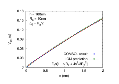
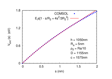
For an HECP emitter, the end cap geometry follows the parabolic approximation of Eq (7) upto . Since field emission at moderate fields ( V/nm) is largely restricted to the region , we present in Fig. (1) a comparison at . The total height of the emitter is nm while the height of the cylindrical post is 50nm. The hemiellipsoid endcap has a height 50nm and apex radius of curvature 10nm. Clearly, within the tunneling distance (typically nm), the analytical expression given by Eq. (37) and Eq. (36) are in good agreement with the exact results.
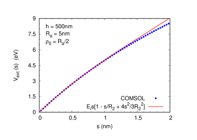
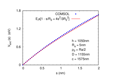
The hemisphere on a cylindrical post is a special case of the HECP emitter. When the hemiellipsoid endcap height is typically five times the apex radius of curvature or greater, the parabolic approximation closely follows the emitter shape till . As the hemiellipsoid height decreases compared to the apex radius, this domain of validity shrinks. When the height of the hemiellipsoid equals the apex radius (hemisphere endcap), the parabolic approximation follows the hemisphere for . Thus, Eqns. (37) and Eq. (36) are not expected to as good at . Fig (2) however shows that there is a fair agreement between Eq. (37) and the exact result even for nm and . We have also found Eq. (37) to hold for rounded conical and pyramidal structures as well.
III.2 Anode proximity
The analytical results presented in section II deal with an isolated emitter with the anode far away. While these results can be analytically extended to deal with anode-proximity and shielding due to other emitters, we shall instead test the sanctity of Eq. (37) numerically when the anode is brought near or when the emitter is part of an array.
The presence of anode cannot be neglected in actual field emission current measurements. Also, it is a known fact that the proximity of anode increases the local electric field at the emitter tip. Hence it is worth investigating how the anode proximity affects the external potential.
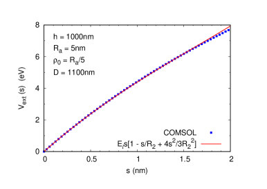
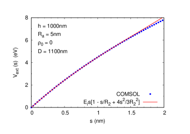
Consider a hemiellipsoidal emitter pin of height nm and tip radius nm, mounted on a grounded conducting plane with anode kept at distance nm from the grounded cathode plane. Thus or the anode is at a distance 100nm from the emitter apex. At locations (i) and (ii) on the surface of a hemiellipsoid, we compare Eq. (37) with the results obtained using COMSOL in Figs.(3) and (4). The agreement is very good in the tunneling region, which implies that the form of external potential is unaltered even with the anode in the close proximity to the emitter. Thus, the external potential follows the same approximate universal trend observed when the anode is far away.
III.3 Emitter array
So far, we have dealt with an isolated emitter with anode at close proximity as well as far away. We now consider the case in which the emitter under consideration is a part of an infinite array. This situation arises when we are dealing with large area field emitters (LAFEs) used in high current applications. In emitter arrays, a notable effect is the reduction in the apex field enhancement factor () compared to that of an isolated emitter. This is attributed to the shielding effects of the neighbouring emitters. The extent of shielding depends on the spacing and configuration of the other emitters in the array.
To study the nature of the external potential in an array, consider HECP emitters of total height nm placed on a square lattice. The cylindrical post of height nm has a hemiellipsoid endcap of height nm and tip radius nm. The lattice constant . Thus, the square domain extends from [-] in both X and Y direction while the HECP emitter is placed at the origin. The anode is kept close at a distance nm. Thus, both shielding and anode-proximity effects are present in this case. The numerical result obtained using COMSOL is compared with Eq. (37) at two locations (i) (Fig 5) and (ii) (Fig. 6). The agreement is found to be good in both cases.
Thus, irrespective of the presence of anode or other emitters in close proximity, the form of external potential is approximately universal in the tunneling region.
III.4 The Tunneling potential
So far we have been discussing the effect of curvature on the potential due to an external applied field. To put things in a proper perspective, it is instructive to look at the full tunneling potential,
| (38) |
seen by the electrons emanating from the emitter tip. As in case of the external potential, the image potential is also affected by the curvature of the tip. The last term in Eq. (38) represents the image-charge potential under a local spherical approximationdb_image .
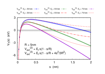
In order to determine the importance of the cubic order correction term in the external potential, we need to compare the tunneling potential with and without the cubic correction over typical tunneling distances involved at various values of the local field as shown in Fig. 7. The notations and in Fig. 7 represent the order of curvature correction and are given by
| (39) | |||||
| (40) |
with the local field at a point in the apex-neighbourhood denoted by and the local second principle radius of curvature denoted by . The value of is taken to be 5nm while three values of the local field are considered in Fig. 7. In computing the tunneling potential, the work function is taken to be eV. Note that at smaller fields, emission occurs close to the Fermi level while at higher fields, the peak of the normal energy distribution shifts further away from the Fermi level swanson ; db_parabolic (see for instance Fig. 4 in Ref. [db_parabolic, ]). Thus, while at V/nm the difference between and is small, at V/nm, the difference in tunneling width is significant for eV. Finally, at V/nm, removing the cubic term clearly makes the barrier unphysical.
Thus, the cubic order corrected external potential form given by Eq (37) is a better approximation. Since a slight change in the tunneling potential can have a magnified impact on the value of transmission coefficient, our calculations show that it is profitable to use a cubic order corrected external potential at least when dealing with emitter tips having radius less than nm at typical local fields of V/nm.
IV Discussions and Conclusions
We have shown, using the nonlinear line charge model, that the external potential has an approximate universal form for sharp emitters irrespective of the particulars of its shape or endcap geometry so long as it is smooth and parabolic in nature. The universal form given by Eq. (37) holds not only on the axis of the emitter, but also away from the axis on the emitter surface. From the numerical studies we found that the Eq. (37) can be applied to a wide generic class of simple as well as complex geometries which need not be well represented by the parabolic approximation for . Also, Eq. (37) was found to be applicable when the emitter is in close proximity to the anode or when it is part of an array.
By knowing the exact form of tunneling potential at all points on the surface of the emitter, one can find the transmission coefficient using approximate techniques such as WKB method, or by numerically solvingdb_vk the Schrödinger equation or even using the transfer matrix methoddb_vk . The total field-emission current from a sharp tip can thus be calculated from a detailed knowledge about tunneling potential. Fortunately, the form of the tunneling potential appears to be approximately universal, independent of the emitter geometry. This should act as an incentive to find approximate analytical expressions for the field emission current densitydb_rr_2021 and even the net emitted current.
V Acknowledgements
The authors acknowledge useful discussions with Dr. Raghwendra Kumar.
Data Availability: The computational data that supports the findings of this study are available within the article.
VI References
References
- (1) N. V. Egorov, E. P.Sheshin Carbon-Based Field Emitters: Properties and Applications in: Gaertner G., Knapp W., Forbes R.G. (eds) Modern Developments in Vacuum Electron Sources. Topics in Applied Physics, vol 135. Springer, Cham.
- (2) G. Fursey, Field Emission In Vacuum Microelectronics, Kluwer/Plenum, New York, 2005.
- (3) K. L. Jensen, Introduction to the physics of electron emission, Chichester, U.K., Wiley, 2018.
- (4) S.-D. Liang, Quantum Tunneling and Field Electron Emission Theories World Scientific Publishing Co. Pte. Ltd., Singapore 2014.
- (5) K. L. Jensen, J. Vac. Sci. Technol. B 21, 1528 (2003).
- (6) R. G. Forbes, App. Phys. Lett. 89, 113122 (2006).
- (7) R. G. Forbes and J. H. B. Deane, Proc. R. Soc. A 463, 2907 (2007).
- (8) J. H. B. Deane and R. G. Forbes, J. Phys. A: Math. Theor. 41, 395301 (2008).
- (9) R. H. Fowler and L. Nordheim, Proc. R. Soc. A 119, 173 (1928).
- (10) L. Nordheim, Proc. R. Soc. A 121, 626 (1928).
- (11) E. L. Murphy and R. H. Good, Phys. Rev. 102, 1464 (1956).
- (12) R. G. Forbes, J. Appl. Phys. 126, 210901 (2019).
- (13) E. O. Popov, A. G. Kolosko, S. V. Filippov, E. I. Terukov, R. M. Ryazanov and E. P. Kitsyuk, J. Vac. Sci. Technol. B 38, 043203 (2020).
- (14) S. Sarkar, R. Kar, J. Mondal, L. Mishra, D. Jayaprakash, N. Maiti, R. Tripathi, and D. Biswas, Carbon Trends 2, 100008 (2021).
- (15) P. H. Cutler, J. He, N. M. Miskovsky, T. E. Sullivan, and B. Weiss, J. Vac. Sci. Technol. B, 11, 387 (1993).
- (16) D. Biswas, G. Singh, S. G. Sarkar and R. Kumar, Ultramicroscopy 185, 1 (2018).
- (17) D. Biswas and R. Ramachandran, J. Vac. Sci. Technol. B 37, 021801 (2019).
- (18) D. Biswas and R. Kumar, J. Vac. Sci. Technol. B 37, 040603 (2019).
- (19) C. Lee, S. Tsujino, and R. J. Dwayne Miller, Appl. Phys. Lett. 113, 013505 (2018).
- (20) A. Chatziafratis, G. Fikioris, J. P. Xanthakis, Proc. R. Soc. A 474:20170692.
- (21) A. Chatziafratis A and J. P. Xanthakis, Journal of Electron Spectroscopy and Related Phenomena 241, 146871 (2020).
- (22) A. Kyritsakis and J. P. Xanthakis, Proc. R. Soc. London, A471, 20140811 (2015).
- (23) D. Biswas, R. Ramachandran and G. Singh, Physics of Plasmas, 25, 013113 (2018).
- (24) E. Mesa, E. Dubado-Fuentes, and J. J. Saenz, J. Appl. Phys. 79, 39 (1996).
- (25) E. G. Pogorelov, A. I. Zhbanov, and Y.-C. Chang, Ultramicroscopy 109, 373 (2009).
- (26) J. R. Harris, K. L. Jensen, and D. A. Shiffler, J. Phys. D 48, 385203(2015).
- (27) J. R. Harris, K. L. Jensen, W. Tang, and D. A. Schiffler, J. Vac. Sci. Technol. B 34, 041215 (2016).
- (28) D. Biswas, G. Singh and R. Kumar, J. Appl. Phys. 120, 124307 (2016).
- (29) D. Biswas, Phys. Plasmas 25, 043113 (2018).
- (30) D. Biswas and R. Rudra, Physics of Plasmas 25, 083105 (2018).
- (31) D. Biswas, Physics of Plasmas, 26, 073106 (2019).
- (32) R. Rudra and D. Biswas, AIP Advances, 9, 125207 (2019).
- (33) D. Biswas, G. Singh and R. Ramachandran, Physica E 109, 179 (2019).
- (34) D. Biswas and R. Rudra, J. Vac. Sci. Technol. B, 38, 023207 (2020).
- (35) D. Biswas, J. Vac. Sci. Technol. B 38, 023208 (2020);
- (36) See for example, R. Whitley, J. Math. Anal. Appl. 105 (1985) 502.
- (37) AC/DC Module User’s Guide, COMSOL Multiphysics v. 5.4. COMSOL AB, Stockholm, Sweden. 2018
- (38) T. A. de Assis and F. F.. Dall’Agnol, J. Vac. Sci. Technol. B 37, 022902 (2019).
- (39) D. Biswas and R. Ramachandran, Physics of Plasmas 24, 073107 (2017).
- (40) L. W. Swanson and A. E. Bell, Adv. Electron. Electron Phys. 32, 193 (1973).
- (41) D. Biswas, Physics of Plasmas 25, 043105 (2018).
- (42) D. Biswas and V. Kumar, Phys. Rev. E 90, 013301 (2014).
- (43) D. Biswas and R. Ramachandran, Higher order curvature corrections to the field emission current density, https://arxiv.org/abs/2103.10075
*
Appendix A Bounds on correction terms
In the following, we shall briefly estimate upper bounds for the correction terms and for a typical emitter with .
A.1 The term
The correction term is
| (41) |
Substituting , and using Bernstein’s inequality,
| (42) | |||||
| (43) | |||||
| (44) | |||||
| (45) |
where . Thus . Generally since the line charge density peaks at . For and , .
A.2 The term
The correction term is
| (46) |
which can in turn be expressed as
| (47) | |||||
| (48) | |||||
| (49) | |||||
| (50) |
For and , .
A.3 The term
The correction term is
| (51) |
which in turn can be expressed as
| (52) | |||||
| (53) | |||||
| (54) | |||||
| (55) |
For and , .