Tailored Light Scattering through Hyperuniform Disorder in self-organized arrays of high-index Nanodisks
Abstract
Arrays of nanoparticles exploited in light scattering applications commonly only feature either a periodic or a rather random arrangement of its constituents. For the periodic case, light scattering is mostly governed by the strong spatial correlations of the arrangement, expressed by the structure factor. For the random case, structural correlations cancel each other out and light scattering is mostly governed by the scattering properties of the individual scatterer, expressed by the form factor. In contrast to these extreme cases, we show here, for the first time, that hyperuniform disorder in self-organized large-area arrays of high refractive index nanodisks enables both structure and form factor to impact the resulting scattering pattern, offering novel means to tailor light scattering. The scattering response from our nearly hyperuniform interfaces can be exploited in a large variety of applications and constitutes a novel class of advanced optical materials.
keywords:
American Chemical Society, LaTeXMLU] Institute of Physics, Martin Luther University Halle-Wittenberg, 06120 Halle, Germany CMAT] Interdisciplinary Center of Materials Science, Martin Luther University Halle-Wittenberg, 06120 Halle, Germany KIT] Institute of Theoretical Solid State Physics, Karlsruhe Institute of Technology, 76131 Karlsruhe, Germany KIT] Institute of Theoretical Solid State Physics, Karlsruhe Institute of Technology, 76131 Karlsruhe, Germany \alsoaffiliation[KITINT] Institute of Nanotechnology, Karlsruhe Institute of Technology, 76021 Karlsruhe, Germany MLU] Institute of Physics, Martin Luther University Halle-Wittenberg, 06120 Halle, Germany \alsoaffiliation[FhG] Fraunhofer Society, 80686 Munich, Germany MLU] Institute of Physics, Martin Luther University Halle-Wittenberg, 06120 Halle, Germany \abbreviationsIR,NMR,UV
keywords: tailored disorder, hyperuniformity, nanophotonics, metasurface.
1 Introduction
Micro- and nanostructured interfaces for electromagnetic scattering continue to play a major role in photonics due to their particularly wide range of existing as well as prospective applications, e.g. for light management in solar cells1, 2, 3 and solid-state lighting devices4, 5, spectral molecular fingerprint detection6, 7, or colored surfaces in architecture and design8, 9, 10. The key challenge in ongoing research is the ability to tailor the optical response from these interfaces in a quite sophisticated manner to meet the demands of specific applications. This fundamental scientific goal is accompanied by the engineering challenge of scalable fabrication of nanophotonic interfaces. As today’s manufacturing capabilities fall far behind proposed theoretical approaches due to the costs and complexity of their fabrication, prevalent structures are those of highest feasibility instead, e.g. in crystalline silicon solar cells pyramidal surface textures by alkaline etching still are industry standard.11 While advanced techniques such as electron beam lithography provide high flexibility in terms of producing nanostructures with quite a deterministic geometry, these fabrication technologies are generally slow and expensive, thus, e.g. applied to solar cells at most feasible for proof-of-concept or research purposes.
In this work, we focus on the implementation of photonic scattering interfaces consisting of an array of identical scatterers. The angle-resolved scattering () response of such a structure generally depends (a) on the arrangement of the scatterers, e.g. regularity of the array and distances between the scatterers, as well as (b) on the properties of the scatterers it is made of, e.g. size, shape, and involved materials. The first property is described by the structure factor , the latter property by the form factor , and under the assumption of the first Born approximation, it is .12, 13 However, either of these two quantities usually determines the angular scattering profile of established scattering interfaces almost completely. The strong spatial correlations present in a periodic array cause the structure factor to compact into a Dirac delta distribution. Hence, scattering from periodic arrays is only allowed into a small fraction of all available angular directions, the well-defined diffraction orders, while any other direction is prohibited as is zero otherwise. A fully random arrangement of scatterers is here in stark contrast. There, no particular direction is enhanced nor suppressed due to the arrangement of the scatterers and the scattering response of the array essentially becomes identical to that of the individual scatterer.
Between these two diametrically opposed types of spatial configurations lies the parameter space of correlated disorder, which received increased interest from the photonics community in recent years.14, 15, 16, 17, 18 On the one hand, a spectrally broadband operation and robustness in fabrication makes the use of disorder attractive. On the other hand, structural correlations enable effective means for directional and spectral enhancement or suppression of scattering. A special class of disorder is the hyperuniform disordered (HuD) case for which large-scale density fluctuations vanish as they do in periodic systems but a disordered and isotropic spatial configuration is maintained.19, 18 HuD structures have recently seen increasing interest in applications and experimental realizations due to their unique properties such as isotropic band gap formation19, 18, 20, 21, 22, 23, 24, 25, 26.
In this work, we will show how a hyperuniform configuration of scatterers enables a new leverage to tailor light scattering by enabling both and to significantly shape the resulting scattering response of the array. The lack of large-scale density fluctuations represents a hidden symmetry and, just as long-range translational symmetry in periodic systems, leads to a strong suppression of small-angle scattering. However, the disorder present in our structures on short length-scales relaxes the bounds of for larger scattering angles up to the extend of random structures, thus leaving the composition of the scattering pattern to .
As scattering elements we choose TiO2 nanodisks. Low-loss high refractive index nanoparticles are renowned for their large scattering cross sections, thus constitute ideal scattering elements for this study27. Furthermore, high-index nanoparticles have received considerable attention from the metamaterials community in recent years as they allow, e.g., the study of magnetic in addition to electrical resonances at optical frequencies.28, 27, 29 These Mie-type resonances give rise to novel ways for near and far field manipulation such as nonlinear frequency generation29, 30 and wavefront shaping31, 32. Nanodisks have been investigated in particular due to their rather simple fabrication while allowing good control over spectral features via the geometry of the disks. Based on findings of our previous work33, in addition to the above we report on a novel scalable method to fabricate substrates covered with TiO2 nanodisk arrays of tailored nearly hyperuniform disorder by a self-organized nanosphere deposition process.
2 Sample fabrication scheme
The procedure to fabricate large-scale TiO2 arrays of tailored disorder relies on a nanosphere deposition technique that we have published elsewhere33. By exploiting the nanospheres as a template in a subsequent dry-etching process, we significantly extend our approach by the ability to obtain disk-shaped nanoparticles. The developed process scheme allows controlled etching of TiO2, which is a material of particular interest to the photonics community due to its high refractive index in the visible spectral range, and is, to the best of our knowledge, here reported on for the first time.
The fabrication scheme (see Figure 1) starts with standard microscopic slides that are functionalized with a Al2O3/TiO2/Al2O3 multilayer with thickness 13.8 nm, 231.0 nm and 19.5 nm, respectively. We use atomic layer deposition (ALD) since this method allows great control over film thickness and produces dense layers. The thin top layer serves a double purpose. Firstly, the surface charges of the Al2O3 film are essential for immobilizing the nanospheres in the subsequent nanosphere deposition. Second, this layer transforms into a hard mask imprinted by the nanospheres. The thick TiO2 layer provides the material of the nanodisks. The thin bottom layer serves as an etch stop to prevent overetching and damage to the substrate.
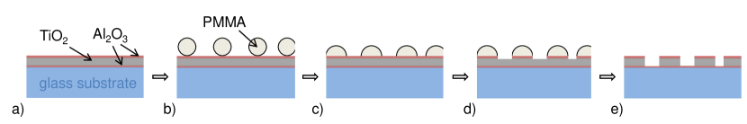
In the next step we apply our nanospheres deposition using PMMA nanospheres (diameter nm) in aqueous dispersion. In short, this technique exploits the electrostatic interactions of surface-charged nanospheres with each other and with the top Al2O3 layer. The nanospheres (negatively charged) are driven towards the substrate (positively charged) and are immobilized as soon as they adsorb on the substrate surface. The nanospheres repel each other, thus modifying the probability of the location of adsorption for another nanosphere. After a certain density of adsorbed nanospheres is reached, no more nanospheres will attach since the repelling forces due to already adsorbed nanospheres become dominant. Therefore, our deposition process is not only self-organized but also self-limiting, which makes it very cost-effective. A prepared dispersion can be applied multiple times since only a tiny fraction of nanospheres is used up during one deposition. By precisely setting the ionic strength of the dispersion, here via the addition of KCl, screening of the nanosphere surface charges within the aqueous dispersion can be controlled, providing an effective lever to control the resulting nanosphere density on the substrate. Details and theoretical background of our nanosphere deposition method are presented elsewhere33.
After the nanosphere deposition, the substrate is rinsed in deionized water and directly transferred to ethylene glycol and heated to 144∘C to slightly soften the nanospheres and increase the particle-substrate bond. This step prevents particle aggregation due to surface tension of the liquid film during drying. After rinsing with water and drying in air, the samples undergo an additional tempering step (30 min at 155∘C) to change the nanospheres’ shape to a dome-like structure such that the area below a nanosphere is fully covered with PMMA (Figure 1c).
The transition from the nanosphere pattern to a Al2O3 hard mask is performed via reactive ion-etching (RIE). As shown by Dekker et al., Al2O3 prepared by ALD provides an excellent hard mask for dry etching processes due to its chemical stability and superior film quality even in thin layers.34 Due to the low volatility of AlF3, Al compounds can not be etched by fluorine-based dry chemistry without a significant physical component. However, they are readily etched in chlorine chemistry.35, 36, 37, 34. Based on this, we developed the hard mask patterning process (see methods section for technical details). The plasma is ignited in a BCl3/Ar atmosphere with a low DC bias to achieve a sufficient Al2O3 over PMMA etching selectivity of 37. The etch rate of Al2O3 was found to be nm/s and the etch time was chosen to be 29 s, which results in slightly overetching the hard mask layer while keeping the PMMA nanospheres sufficiently intact, which are afterwards removed in a pure O2 plasma.
Unlike Al2O3, TiO2 is etched by fluorine chemistry. Based on the work of Choi et al.,38 a CF4-O2-based process has been developed resulting in a TiO2 etch rate of nm/s and a TiO2 over Al2O3 selectivity of . Hence, the top hard mask layer was sufficiently thick. For the 231.0 nm TiO2 layer, we etched for 240 s, i.e. longer than actually needed. However, the Al2O3 etch stop layer beneath limits the etch depth and thereby increases repeatability of the manufacturing process (Figure 1e). The requirements of high selectivity, high aspect ratios and smooth surfaces are difficult to meet in fluorine-based TiO2 etching compared to, e.g., silicon processes 39, 40, as parameters for vertical sidewalls and good selectivity also lead to self-masking effects and, thus, rough surfaces. In our case, etching down to the etch stop layer reduces the roughness to an acceptable level for our investigations and produced relatively smooth surfaces (see Figure 2b) compared to previously published results41, 42. We note that reactive ion etching processes have been successfully applied in industrial process chains and therefore do not principally impede the scalability of our fabrication method 43, 44.
3 Results and discussion
The key objective of this study is to combine scattering properties of the individual TiO2 nanodisk (form factor ) with those introduced by positional correlations of their disordered arrangement (structure factor ). Therefore, we choose the dimensions of the nanodisks, diameter and height , and the characteristic distance of the array, i.e. the typical next-neighbor center-to-center distance defined as the first maximum of the pair correlation function of the array19, such that the resulting spectral features overlap. Given the refractive index of our amorphous TiO2, 2.54 - 2.31 for a wavelength range of , preliminary calculations using the finite-element method (FEM) predict a number of multipolar resonances in the visible and near-infrared spectral region for individual nanodisks of about 230 nm height and 500 nm diameter. Accordingly, the nearest available particles size from stock, nm, was chosen for the template fabrication. For the structural resonances to spectrally coincide with the resonances of the individual nanodisks, needs to be of the same order as the wavelength. We have previously demonstrated how can be varied by the deposition conditions. Furthermore, we are able to statistically predict particle patterns based on a modified random sequential adsorption (RSA) model of soft spheres near the saturation density.33 Thus, we experimentally fabricated a set of samples comprising glass substrates covered with disordered TiO2 nanodisk patterns with desired geometrical dimensions. Additionally, one pattern that ideally shows no structural correlations, i.e. of random disorder, was fabricated by exposing the functionalized substrate to the nanosphere dispersion for only a short period of time such that the particle density is far from saturation. In the following we discuss the properties of such samples first from a structural and later from an optical perspective.
3.1 Structural properties
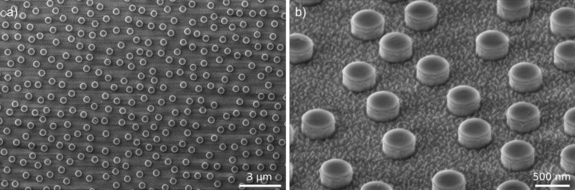
We successfully fabricated disordered arrangements of TiO2 nanodisks. Exemplary images of the fabricated TiO2 nanodisk structures are shown in Figure 2. We determine an average nanodisk diameter of 455.0 5.4 nm and an average height of 231.0 nm. We attribute the nanodisk diameter dispersion to the size dispersion of the nanospheres used to prepare the mask template. In comparison to the nanospheres (499 nm diameter), the disks are around 10 % smaller in diameter, which is a result of the tempering process prior to pattern transfer. The error on disk height is negligible due to the excellent control of ALD deposition over layer thickness.
The disks are homogeneously distributed across the entire substrate surface in a disordered pattern (see characterization methods for pattern extraction) The statistics of our patterns can be appropriately captured in Fourier space. We consider the size dispersion of the disks sufficiently small to consider the structure factor instead of the spectral density. However, the latter would be a more appropriate quantity to characterize polydisperse particle patterns 45. The (static) structure factor of a -point pattern is 46, 47
| (1) |
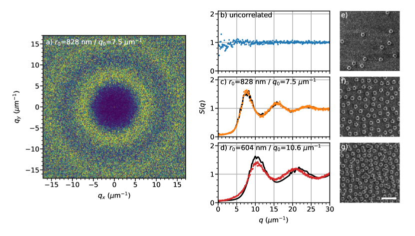
with wave vectors . In this work, we write for wave vectors that lie in the plane of the nanodisk array and for wave vectors of propagating free-space light modes which in general have a component perpendicular to the array plane. The point patterns are isotropic, thus is rotationally symmetric, exemplary shown in Figure 3a. The angular average is plotted for typical samples in Figure 3b-d together with of predicted patterns.
Figure 3b shows for the sample on which the nanosphere deposition was stopped prior saturation. As a result, spatial correlations are negligible and for all and we will refer to this pattern in the following as uncorrelated. The deviation from unity near stem from the fact that particles maintain a minimum distance, which becomes relevant at finite densities. However, the random nature of the process prevails.
The particle patterns of the samples corresponding to Figures 3c and d are saturated and reveal strong correlations, i.e. clearly deviates from unity. Each structure factor of these patterns holds a characteristic peak at around m-1 and m-1, corresponding to a characteristic next-neighbor distance of about nm and nm, respectively, that is also indicated in the figure. For the sparsely coated saturated sample (Figure 3c,f), we find excellent agreement between our modified RSA model 33 and experiment, whereas for the densely coated sample (Figure 3d,g) a lower value of and a slight shift of about m-1 compared to the prediction can be observed. A possible explanation for this deviation in the denser sample is the occurrence of aggregates, i.e. touching particles, which is not accounted for in our deposition model. To experimentally achieve a certain characteristic distance , we carefully adjust the electrostatic potential landscape in which the nanospheres move through during the deposition process and a rather shallow potential minimum (in the order of ) gives rise to a preferred next neighbor distance.33 However, as soon as two spheres touch each other, irreversible aggregation occurs. Thus, the smaller the characteristic distance aimed for, the higher the probability of aggregate formation, which is supported by our observations in numerous other experiments. Furthermore, aggregates would also explain increased values of for in comparison to our model, as aggregate formation occurs in a random Poisson-like manner and, therefore, enhances long-range particle density fluctuations. Therefore, aggregation and its effect on the resulting structure factor should be taken into account when considering high particle densities. For the samples used in this work, the number share of particles present in configurations of two or more touching particles was found to be 2.6 %, 3.0 %, 9.5 %, and 31.2 % for nm, 713 nm, 649 nm, and 604 nm, respectively. Due to the strong increase in aggregation for nm, the pattern may be dubbed over-saturated. Nevertheless, the general shape of the structure factor is still preserved (Figure 3d). Furthermore, we note that the final structure was obtained by patterning a flat layer. Therefore, all nanosphere aggregates result in in-plane nanodisk aggregates, i.e. a binary height profile with no component in the third dimension.
For our samples of correlated disorder, becomes small for approaching zero, which is equivalent to a suppression of density fluctuations on large length scales. When , structures are referred to as hyperuniform, and stealthy hyperuniform when vanishes for an entire range of around the origin.48, 19 In real world structures, the strict criterion of can obviously not be achieved due to fundamental aspects such as finite size and temperature effects to the least. A practical criterion that has recently been proposed is the hyperuniformity metric49, 19
| (2) |
A system is considered as effectively hyperuniform if is of the order of 49, which is stricter than the requirement for nearly hyperuniform patterns with on the order of 50. In our case, and the lower limit of the structure factor is , which is slightly lower than values found for 2D random sequential adsorption of hard sphere patterns51. Therefore, we consider the structures shown here nearly hyperuniform disordered.
Besides fundamental reasons, we suspect further limitations similar to those applying to conventional RSA patterns hindering the achievement of lower degrees of hyperuniformity. In RSA patterns, a strictly sequential adsorption of particles onto the substrate surface is assumed and except the condition that particles must not overlap no interaction potential is accounted for. Thus, the precise position of an adsorbed particle carries a rather large amount of randomness leading to density fluctuations at large length scales, i.e. . In our case, the particles interact with each other via repulsive electrostatic and attractive van-der-Waals forces33. The probability for a particle to adhere in the vicinity of already attached particles with a characteristic distance -which we are able to set experimentally- is therefore modulated and leads to increased correlations of particle positions. Additionally, the adsorption of particles is not strictly sequential so there might be some degree of coordination while particles are mobile. However, the particle ensemble cannot achieve a collective configuration to minimize potential energy since they are immobilized as soon as they touch the substrate. Thus, density fluctuations are not fully suppressed and it can therefore be assumed that in our nanosphere deposition will be at least identical or, as observed here, smaller to the RSA case. At this point, the limits of in self-organized bottom-up techniques like ours are still an open question. Nevertheless, the relative stealthiness of our patterns, i.e. being rather small for a range of ’s around the origin, has a strong impact on their scattering properties as we will show in the next section.
3.2 Optical properties
3.2.1 Numerical method
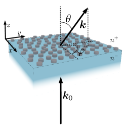
To numerically reproduce the optical response of our fabricated TiO2 nanodisk arrays, we apply the first Born approximation,12 i.e. the exciting light field for each scatterer is assumed to be the unperturbed incoming light field . Throughout this work we consider plane wave irradiation through a transparent substrate of refractive index occupying the half space. The half space is vacuum with , see Figure 4 for notation. The plane wave with field amplitude is -polarized and normally incident onto an infinite array of identical scatterers covering the substrate, i.e. .
The scattered far field () of an individual scatterer can be expressed as an outgoing spherical wave (we omit the harmonic time dependence in the following)
| (3) |
is the form factor and describes the normalized scattered field amplitude of an individual scatterer for a given polarisation and incoming and scattered wave vectors and , respectively. Furthermore, is the differential scattering cross section or radiation pattern of the individual particle. can be readily obtained by various means, e.g. analytically by Mie theory in case of a spherical particle, or by rigorously solving Maxwell’s equations with techniques such as FEM. We write for -polarized irradiation normal to the array plane, i.e. . Using the angular spectrum representation of Equation 3 in its asymptotic limit (),52 we find the normal incidence transmission and reflection of an infinite array of identical scatterers in terms of the form factor to be
| (4) | |||||
| (5) |
with areal density of scatterers , Fresnel’s transmission and reflection coefficients and of the bare substrate interface, wave numbers and in substrate and vacuum, and , respectively.
Scattering into the directions normal to the array plane, , depends on and , but not on the particular spatial arrangement of scatterers. Interference of these fields with and (Equations 4 and 5) determines the normalized power that undergoes off-normal scattering, (neglecting absorption). However, for off-normal scattering structural phase relations have to be accounted for by modulating by the structure factor , with the projection of the scattered wave vector onto the array plane.13 Using , with integration of the angle-resolved scattering over the unit sphere except for , we can now write down the response of the array at normal incidence as
| (6) |
The numerical approach described here significantly simplifies the computational efforts to predict the optical response of our structures. The structure factor in Equation 6 can be taken either from experiment, e.g. by evaluating SEM pictures, or, if sufficient knowledge of the fabrication process is available, from theoretical modelling such as our modified RSA approach.33 Instead of numerically solving Maxwell’s equations for a computational domain large enough to sufficiently approximate the statistics of a disordered array of scatterers, only the scattering response of the individual scatterer is calculated rigorously. We shortly discuss the applicability of the first Born approximation to our structures at the end of the discussion, see below.
3.2.2 Angle-resolved scattering response
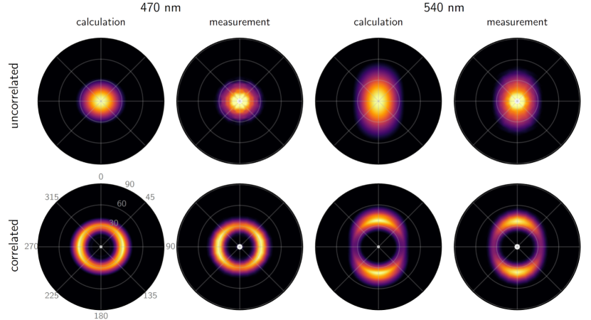
Figure 5 illustrates how arranging identical TiO2 nanodisks into a nearly HuD pattern has a remarkable impact on the resulting angular scattering response. For two different wavelengths we compare the of the uncorrelated pattern in the top row and a nearly HuD pattern (characteristic distance nm) in the bottom row. Additionally, corresponding numerical results after the approach described above are plotted using calculated by FEM and taken from our modified RSA modelling algorithm.
For the uncorrelated sample, it is for all ’s (see Figure 3b), thus its essentially remains that of the individual nanodisk but scaled by the number of illuminated particles. Scattering is strongest at and quickly decreases as increases. In contrast to this, scattering is very different for the nearly HuD pattern with a maximum at significantly larger angles and being mostly confined within a ring-shaped area. Spatial correlations in these structures, e.g. expressed through the existence of the characteristic distance of neighbors , leads to similar optical phase differences for off-normal scattered light waves. Thus, destructive as well as constructive interference occurs and even though translational symmetry is missing, intensity maxima (ring-shaped area) or minima (angular area inside ring) appear well pronounced. Opposed to the well-know diffraction of an optical grating, which is based on interference as well, constructive interference occupies a much larger solid angle due to a range of similar but not exactly equal distances between scatterers. E.g., for nm we find that % of forward scattering is confined within for the uncorrelated case, while the same amount is confined within for the nearly HuD case.
In contrast to irradiation with unpolarized light, we here observe experimentally as well as numerically a -dependency of the scattering response, which is very subtle for most part of the investigated spectral range but is slightly visible at nm and well observed for nm. In particular, for the nearly hyperuniform sample it can be seen that for nm scattering reaches out further into the - than into the -direction, and even more pronounced for nm but perpendicular to the former, i.e. reaching out further into the - than into the -direction. The same anisotropy is also present for the uncorrelated sample, but less pronounced.
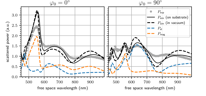
To elucidate our observations, we look into the -dependency in more detail in Figure 6. Plotted is the power scattered into the - and -plane in forward direction, with and 90∘, respectively, and , and of the uncorrelated sample together with FEM simulations of a single TiO2 nanodisk on glass substrate. Furthermore, we performed a multipole expansion analysis of a single TiO2 nanodisk. As multipole expansion is only defined for a scatterer embedded in a homogeneous medium, we analyse a TiO2 nanodisk with identical geometrical dimensions in vacuum (dashed lines). Comparing for the isolated disc in vacuum with the case of the disk on glass substrate, we find only minor deviations, particularly for the spectral feature at nm. This indicates that the removal of the substrate has only little impact on the optical properties of the disk and insights obtained from the multipole expansion considering the isolated disc can be applied to the substrate case.
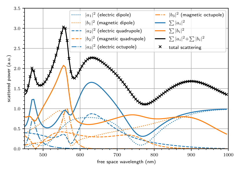
The multipole expansion reveals that for our chosen nanodisk dimensions a plethora of modes ranging from magnetic and electric dipoles up to octupoles contribute significantly to the scattering response withinin the spectral range of interest (see Figure S1 in supporting information). None of the spectral features found in the scattering spectra can be accounted to a single mode but a mix of several modes. However, comparing the power emitted by the sum of electric dipole, quadrupole, and octupole with the sum of their magnetic counterparts, and , respectively (colored dashed lines in Figure 6), reveals that scattering at nm is predominately caused by electric modes, whereas at nm it is predominately caused by magnetic modes.
The electric moments excited in the nanodisks share an equatorial plane that is oriented perpendicular to the one shared by the magnetic moments, according to the geometry of our experiment the - and the -plane, respectively. Therefore, since their equatorial planes are also the planes of preferred scattering, excitation of these two kind of modes explains the observed -anisotropy observed in Figure 5. However, as both kind of modes emit into small s, the discussed effect is only significant at larger s. As scattering concentrates at rather small s for the uncorrelated case, the dependency of the scattering pattern on the nature of the excited mode is only weak. But arranging the same nanodisks into a nearly HuD pattern strongly emphasizes this effect. Due to its structure factor, small-angle scattering is suppressed, hence giving an enhanced spatial contrast to differentiate between the nature of the excited modes. To be specific, for TiO2 disks arranged in an uncorrelated pattern the ratio at nm is 2.2, but it more than doubles to 5.2 in the nearly HuD case.
3.2.3 Spectral dependence of scattering response
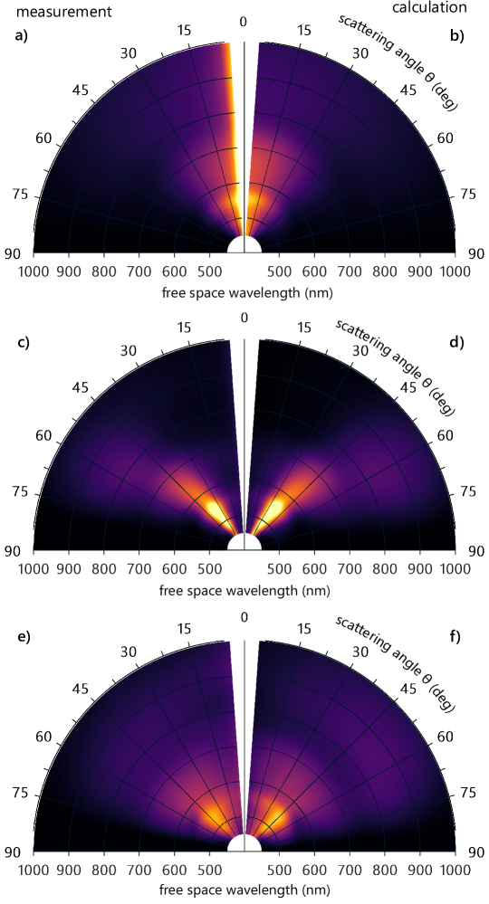
In Figure 7, we capture the spectral dependence of scattering in near HuD TiO2 nanodisk arrays by plotting the calculated and experimentally measured against wavelength and forward scattering angle . As the -dependency was discussed in the previous section and for the sake of clarity, the values are averaged over . The top row shows the scattering response of the uncorrelated array, i.e. essentially the unmodified response of the individual TiO2 nanodisk, the centre and bottom rows show the scattering response of two nearly HuD arrays with different characteristic distances nm, and nm, respectively. Both of them have been discussed in Figure 3. As indicated above for single wavelengths, experimental and calculated ARS agree as well for the whole considered spectral range.
The unmodified scattering response of the uncorrelated pattern is characterized by spectrally broadband forward scattering with its maximum at . The strongest scattering response is around nm, which can be attributed to the simultaneous excitation of the magnetic dipole, quadrupole, and octupole mode (see also supporting information, Figure 9). The center row of Figure 7 shows the scattering response of the nearly HuD sample that was also under study in the previous section. In accordance to the observations for single wavelengths, the ARS is modified for the whole considered spectral range as well, i.e. transformed into a ring-shaped pattern with a scattering maximum . Surprisingly, the angular range covered by the ring stays almost constant for a rather large spectral bandwidth. To be precise, for nm the major part of scattered light stays within , for nm, the ring radius rather abruptly increases to occupy an angular range of .
Scattering in both periodic and (nearly) HuD structures is based on structural phase-induced interference, therefore it is intuitive to compare the two. In Figure 8a we plot the same as in Figure 3c but converted to the corresponding scattering angle for each wavelength . Since is a property of the arrangement of scatterers within the array, it is invariant with regards to constant ’s, and, thus, its course for varying and is determined through (assuming normal incidence). This general relation is fundamental for periodic structures, such as optical gratings, since it sets the only angular directions periodic structures are allowed to scatter into as long as exactly equals a multiple of reciprocal grating vectors. The black line in Figure 8a follows of the HuD array. Considering a periodic pattern with periodicity , this line would also represent its (first) diffraction order. The most distinct difference between of a periodic and a HuD structure is that the first consists of a set of Dirac delta functions while the latter is a continuous function. This implies the existence of a cutoff wavelength for the periodic structure, i.e. for wavelengths , off-normal scattering is disabled since then all scattered waves become evanescent in the normal direction. In contrast to this, the continuous nature of of a HuD structure leads to a pronounced spectral broadening of any features of as clearly visible in Figure 8a. For , i.e. when light with wavelengths longer than the one corresponding to , non-vanishing values of still stretch over a considerable angular and spectral range enabling scattering. For example, light waves corresponding to are able to propagate in free space up to nm. In case of a truly stealthy HuD structure, for which for some finite , a cutoff wavelength exists as well, but in contrast to the periodic case, this wavelength can in principle be much longer than the characteristic next-neighbor distance of scatterers within the array.
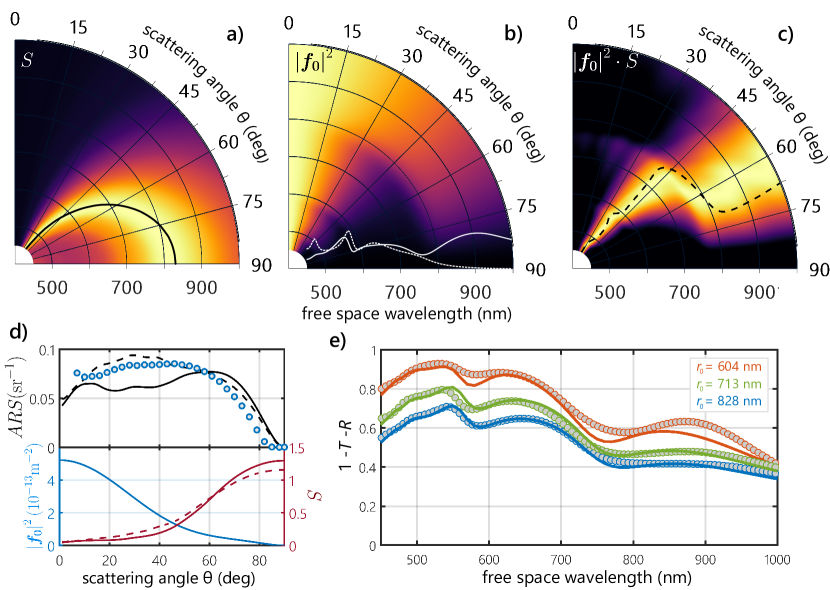
However, by comparing Figure 7c/d and Figure 8a, the cannot be traced back to the structure factor alone. Indeed, we find that the form factor has to be taken into account as well. In Figure 8b we plot the radiation pattern of the individual nanodisk. Since we focus on the angular dependence for now, is normalized by its maximum value for each wavelength, i.e. by its value in forward direction (). In this representation, the angular dependencies of the different involved multipoles become visible. For nm, scattering is confined roughly within but abruptly widens up to for nm. Multipole expansion analysis reveals that this is due to the electric and magnetic dipole modes being the dominant modes excited in our nanodisks for nm (see overlayed full and dashed white lines in Figure 8b). The resulting scattering pattern of the individual nanodisk depends on the detailed interference of all excited multipoles53. In contrast to higher order modes, such as quadrupole and octupole modes, the radiation pattern of pure dipole modes does not hold a -dependence, i.e. does not posses any radiation lobes. Therefore, as long as dipole modes are dominant their radiation pattern is only little affected by interference with higher-order modes and they keep their angularly broad scattering. This is not the case for nm, as electric and magnetic quadrupoles as well as octupoles are excited, resulting in a scattering pattern that is confined to a smaller -range.
The final of scatterers with form factor arranged into an array with structure factor is proportional to their product, (Equation 6), which we plot in Figure 8c. Essentially, this is the same data as shown in Figure 7d, but again we normalize to the maximum value at each wavelength to better visualize the resulting main direction of scattering. Additionally, a contour line of the normalized radiation pattern of the individual nanodisk (Figure 8c) is overlayed following the value of at the absolute scattering maximum of this sample, ( nm, , see Figure 7d). In this representation, it becomes visible that the angular scattering properties of our nearly HuD structures is indeed not only governed by . Comparing the contour line and the course of maximum scattering (light-yellow regions in Figure 8c) reveals that the angular dependence of the individual scatterer is clearly imprinted into the angular dependence of the array.
This is in stark contrast to diffraction in periodic structures. In these, the impact of is limited to the intensity of a diffraction order, but never affects the direction of propagation. However, our observations are as well in contrast to truly random structures, in which alone determines the scattering pattern since in those structures is . In fact, instead either or dominating the scattering response, tailored disorder structures such as our HuD structures enable a precise interplay between and .
An example of how delicate this interplay can be reveals another sample with the same TiO2 nanodisks but different characteristic distance nm. Its experimentally measured is plotted in Figure 7e and we observe a rather uniform scattering response with regards to and . With from our modified RSA modelling we were not able to theoretically reproduce the as good as it is the case for the other samples. We found better agreement using the experimentally evaluated (deduced from SEM pictures), the resulting is shown in Figure 7e. This can also be observed in Figure 8d, where we plot , , and the resulting for nm. It can be recognized how the slight deviations between simulated (full line) and experimental (dashed) lead to a closer agreement between of theory and experiment. The need to use the experimental is due to the high share of aggregates (30.2%) in this sample as pointed out above in the discussion on structural properties. The occurence of aggregates is random, which shifts slightly towards unity and, for the case shown in Figure 8d, increases scattering up to .
We point out that many experimentally obtained disordered interfaces generally carry intrinsic correlations to some extend due to fabrication conditions and constraints, i.e. , or any other appropriate representation of a structure in Fourier space, deviates from the value of a truly random structure. As an example, it is known that black silicon surface textures prepared by dry-etching have certain correlation lengths that can be controlled through fabrication parameters, moreover, it has been shown that their correlation length correlates with the light-trapping abilities of these kind of textures in solar cells54, 2. However, as long as has no tendency towards zero for and concentrates scattering into an angular region of small ’s, which is the case for most nanoparticles commonly used in the field of nanophotonics, these structures will still scatter mostly into the forward direction since their and are both large. To suppress scattering into small s, has to be as small as possible in the corresponding -range, but large otherwise, which essentially describes of a nearly HuD structure. Therefore, we can identify (nearly) HuD as a key element to achieve high efficiency large-angle scattering.
Concerning array properties, specular transmission and reflection depend only on the areal nanodisk density but are independent of , see Equations 4 and 5. This counter-intuitive result is a direct consequence of the first-Born approximation which we apply within the framework of our numerical approach, as it neglects any kind of coupling between scatterers that could change in, e.g., dependence of distance to neighboring scatterers. However, throughout this work and also in Figure 8e, where we plot for different nearly HuD samples made of the same nanodisks but different and , we find good agreement between numerical and experimental results. We take the observed agreement as a strong indication that the assumption of negligible inter-particle coupling in our samples is sufficiently justified. We attribute the deviations between the numerical and experimental values in case of the dense sample (orange) in Figure 8e to the high number of aggregates in this sample.
However, since depicts the amount of light scattered, but does not imply how the angular scattering response looks like, Figure 8e also reveals the potential of (nearly) HuD structures to built highly efficient scattering interfaces with a scattering response on demand (see also supporting information). The scattering response is up to the interplay between and and can be tailored by adapting both precisely. It implies that one could change by using another scatterer geometry, and by refining the fabrication process to suppress the occurrence of aggregates at high densities and enhance hyperuniformity, or use even another suitable process to enable the fabrication of desired .
4 Conclusion
In summary, we achieved to prepare high-index nanodisk arrays of strong correlated disorder with a novel fabrication method. The developed technique is scalable and allows control over important properties of the array, such as nanodisk height and diameter, and characteristic next-neighbor distance, through easy-to-access experimental parameters. Moreover, we could show that the disorder of the arrangement of the nanodisks is nearly hyperuniform, leading to rather unusual light scattering properties. While control over the angular scattering response of conventional scattering interfaces, either periodic or random, is essentially limited by either the structure or the form factor, near hyperuniform disorder enables both quantities to substantially impact the response. This particular ability, in consequence, leads to a fundamentally novel approach to tailor light scattering through tailoring both structure and form factor towards a scattering response on demand and paves the way to a new class of optical materials.
5 Methods
5.1 Nanodisk array fabrication
Standard 1 mm thick 76 x 26 mm object slides (soda-lime glass) were coated by thermal atomic layer (ALD) deposition in a Beneq TFS-200 ALD tool. First, the 13.8 nm etch stop layer of Al2O3 was deposited by alternating pulses of trimethylaluminum (Al(CH3)3) and water (250 ms pulse duration, 100 pulses per precursor, 3 s purge) at 180∘C55. Then, a 231.0 nm layer of TiO2 was deposited at 120∘C by 3633 alternating pulses of TiCl4 and water (pulse duration 200 ms). This layer provides the material the nanodisks are made of. In more detailed studies on the optical properties of ALD grown TiO2 found in literature,56, 57, 58 deposition temperatures below C produce smooth, amorphous films with negligible optical losses in the visible spectrum compared to higher deposition temperatures, which agrees well with our observations by electron microscopy and spectroscopic ellipsometry. To complete the layer stack (please note Figure 1a), a layer of 19.5 nm Al2O3 was deposited by ALD (165 cycles, otherwise same deposition parameters as above).
A dispersion of PMMA nanospheres with diameter of 499 10 nm (microParticles GmbH, Berlin, Germany) was first treated in an ultrasonic bath for 30 min to break up reversible aggregates and then diluted with a mixture of MicroPure water (18 Mcm) and 30 % isopropyl alcohol (p.a. grade). Potassium chloride (KCl) was used to carefully adjust the ionic strength of the dispersion (typically in the range of M to M). The ALD coated substrates were exposed to the dispersion for 18 hours and rinsed in deionized water afterwards. The samples were then rinsed in ethylene glycol multiple times to remove all water since Al2O3 surfaces can degrade in hot aqueous solutions during the subsequent tempering step 59.
Pattern transfer was performed via RIE in an Oxford Plasmalab 100 System. For the Al2O3 etch process, BCl3 and Ar were used in a ratio of 30:20 sccm at a pressure of 10 mTorr. The inductively coupled plasma (ICP) power was 2500 W and the capacitively coupled plasma (CCP) power was 63 W, resulting in a dc-bias of -89 V 37. For the TiO2 etch process the gas of CF4:O2:Ar was 40:6:10 sccm with the pressure kept constant at 15 mTorr. The ICP power was 1800 W and the CCP power was 41 W, resulting in a dc-bias of -81 V.
5.2 Characterization
For the microstructural characterization, SEM images were recorded with a field emission microscope (FEI Versa 3D) at 4 kV. Disk positions were extracted from images of 104 x 70 m2 areas via template matching33, 60. Some disk pairs exhibit nominal surface-to-surface distances nm (see e.g. Figure 3g) due to slight merging of the PMMA particles during tempering. Those pairs were defined as disks in aggregates.
The ALD layers were optically characterized on Silicon reference samples using a spectroscopic ellipsometer (J.A. Woollaam M2000V). Due to the low absorption of TiO2 the refractive index could reasonably approximated by Cauchy’s equation with , e.g. 2.54 and 2.31.57, 58
Angular resolved scattering measurements were performed using a custom-made goniometer setup. White light of a halogen lamp was collimated, linearly polarized (where applicable) and directed onto the respective sample. The scattered light was collected and focused onto a fiber bundle by a single lens with an aperture corresponding to an acceptance angle of . Accordingly, the lense-fiber setup was rotated about the sample from (to avoid recording the directly transmitted light) to in steps of . A monochromator (Horiba iHR550) in conjunction with a silicon photodetector (Thorlabs DET210) and a lock-in amplifier (Stanford Research Systems SR830) was used to detect the light at the fiber output in the range of 450 nm to 1000 nm. Directly transmitted light at without sample was recorded as reference for each linear polarization angle and for unpolarized light, in order to characterize the system response. The presented data are . Integrations over the forward-scattering half-space were , where the accounts for stronger representations of larger angles.
5.3 Numerical methods
Point configurations were predicted via a random sequential adsorption scheme in a Monte Carlo type code. The soft-sphere behavior of the charged colloidal particles was taken into account by modulating the probability of a particle to adhere on the substrate at a given random position within an extended radius of neighboring particles33. Considering the extended radius, the saturation density in the experiment was slightly higher than in the hard-sphere case but approximately constant over a variety of number densities. It could therefore be kept constant for the prediction of patterns. Optimizations of the algorithm regarding computation time were inspired by the work of Zhang et al.51
To calculate the angular resolved scattering response of a single nanodisk, the form factor , we rigorously solved Maxwell’s equations in 3D with appropriate source, material, and boundary condition settings using the time-harmonic finite-element solver JCMsuite61. To obtain the angular resolved scattering response of an infinitely extended array of identical nanodisks, is combined with the structure factor of the point configuration of the particular array via our numerical approach based on Born’s approximation (Equations 4-6). Multipole decomposition was performed using an integrated function of JCMsuite that applies the multipole expansion to the scattered fields and solves for the corresponding coefficients using an algorithm presented by Santiago et al.62
This work was funded by the Deutsche Forschungsgemeinschaft (DFG) through program DFG-SPP 1839 “Tailored Disorder”, second period (RO 3640/6-2 and WE4051/19-2, project 278744673). The authors thank Claudia Stehr for her excellent technical support.
References
- Spinelli et al. 2012 Spinelli, P.; Verschuuren, M.; Polman, A. Broadband Omnidirectional Antireflection Coating Based on Subwavelength Surface Mie Resonators. Nat. Commun. 2012, 3, 692
- Otto et al. 2015 Otto, M. et al. Black Silicon Photovoltaics. Adv. Opt. Mat. 2015, 3, 147–164
- Schneider et al. 2020 Schneider, T.; Tröndle, J.; Fuhrmann, B.; Syrowatka, F.; Sprafke, A.; Scheer, R. Ultrathin CIGSe Solar Cells with Integrated Structured Back Reflector. Solar RRL 2020, 4, 2000295
- Son et al. 2012 Son, J. H.; Kim, J. U.; Song, Y. H.; Kim, B. J.; Ryu, C. J.; Lee, J.-L. Design Rule of Nanostructures in Light-Emitting Diodes for Complete Elimination of Total Internal Reflection. Adv. Mat. 2012, 24, 2259–2262
- Park et al. 2020 Park, J. Y.; Kim, B. J.; Yoo, C. J.; Dong, W. J.; Lee, I.; Kim, S.; Lee, J.-L. Subwavelength-scale nanorods implemented hexagonal pyramids structure as efficient light-extraction in Light-emitting diodes. Sci. Rep. 2020, 10, 2045–2322
- Ding et al. 2016 Ding, S.-Y.; Yi, J.; Li, J.-F.; Ren, B.; Wu, D.-Y.; Panneerselvam, R.; Tian, Z.-Q. Nanostructure-based plasmon-enhanced Raman spectroscopy for surface analysis of materials. Nat. Rev. Mat. 2016, 1, 16021
- Langer et al. 2020 Langer, J. et al. Present and Future of Surface-Enhanced Raman Scattering. ACS Nano 2020, 14, 28–117
- Chung et al. 2012 Chung, K.; Yu, S.; Heo, C.-J.; Shim, J. W.; Yang, S.-M.; Han, M. G.; Lee, H.-S.; Jin, Y.; Lee, S. Y.; Park, N.; Shin, J. H. Flexible, Angle-Independent, Structural Color Reflectors Inspired by Morpho Butterfly Wings. Adv. Mat. 2012, 24, 2375–2379
- Bläsi et al. 2017 Bläsi, B.; Kroyer, T.; Höhn, O.; Wiese, M.; Ferrara, C.; Eitner, U.; Kuhn, T.-E. Morpho butterfly inspired coloured BIPV modules. Proc. 33rd EU PVSEC 2017, 2630–2634
- Liu et al. 2020 Liu, X.; Huang, Z.; Zang, J. All-Dielectric Silicon Nanoring Metasurface for Full-Color Printing. Nano Letters 2020, 20, 8739–8744
- Wilson et al. 2020 Wilson, G. M. et al. The 2020 photovoltaic technologies roadmap. J. Phys. D: Appl. Phys. 2020, 53, 493001
- Born et al. 1999 Born, M.; Wolf, E.; Bhatia, A. B.; Clemmow, P. C.; Gabor, D.; Stokes, A. R.; Taylor, A. M.; Wayman, P. A.; Wilcock, W. L. Principles of Optics: Electromagnetic Theory of Propagation, Interference and Diffraction of Light, 7th ed.; Cambridge University Press, 1999
- Zemb and Lindner 2002 Zemb, T.; Lindner, P. Neutron, X-rays and Light. Scattering Methods Applied to Soft Condensed Matter; North-Holland, 2002
- Vynck et al. 2012 Vynck, K.; Burresi, M.; Riboli, F.; Wiersma, D. S. Photon Management in Two-Dimensional Disordered Media. Nature Mat. 2012, 11, 1017–1022
- Wiersma 2013 Wiersma, D. S. Disordered photonics. Nat. Photonics 2013, 7, 188–196
- Rockstuhl and Scharf 2013 Rockstuhl, C., Scharf, T., Eds. Amorphous Nanophotonics; Nano-Optics and Nanophotonics; Springer Berlin Heidelberg: Berlin, Heidelberg, 2013
- Riboli et al. 2014 Riboli, F.; Caselli, N.; Vignolini, S.; Intonti, F.; Vynck, K.; Barthelemy, P.; Gerardino, A.; Balet, L.; Li, L. H.; Fiore, A.; Gurioli, M.; Wiersma, D. S. Engineering of light confinement in strongly scattering disordered media. Nature Mat. 2014, 13, 720–725
- Yu et al. 2020 Yu, S.; Qiu, C.; Chong, Y.; Torquato, S.; N., P. Engineered disorder in photonics. Nat. Rev. Mater. 2020,
- Torquato 2018 Torquato, S. Hyperuniform States of Matter. Phys. Rep. 2018, 745, 1–95
- Sun et al. 2018 Sun, M.-J.; Zhao, X.-Y.; Li, L.-J. Imaging Using Hyperuniform Sampling with a Single-Pixel Camera. Opt. Lett. 2018, 43, 4049
- Castro-Lopez et al. 2017 Castro-Lopez, M.; Gaio, M.; Sellers, S.; Gkantzounis, G.; Florescu, M.; Sapienza, R. Reciprocal Space Engineering with Hyperuniform Gold Disordered Surfaces. APL Photonics 2017, 2, 061302
- Leseur et al. 2016 Leseur, O.; Pierrat, R.; Carminati, R. High-Density Hyperuniform Materials Can Be Transparent. Optica 2016, 3, 763
- Florescu et al. 2009 Florescu, M.; Torquato, S.; Steinhardt, P. J. Designer Disordered Materials with Large, Complete Photonic Band Gaps. PNAS 2009, 106, 20658–20663
- Man et al. 2013 Man, W.; Florescu, M.; Williamson, E. P.; He, Y.; Hashemizad, S. R.; Leung, B. Y. C.; Liner, D. R.; Torquato, S.; Chaikin, P. M.; Steinhardt, P. J. Isotropic band gaps and freeform waveguides observed in hyperuniform disordered photonic solids. PNAS 2013, 110, 15886–15891
- Florescu et al. 2013 Florescu, M.; Steinhardt, P. J.; Torquato, S. Optical cavities and waveguides in hyperuniform disordered photonic solids. Phys. Rev. B 2013, 87, 165116
- Milosevic et al. 2019 Milosevic, M. M.; Man, W.; Nahal, G.; Steinhardt, P. J.; Torquato, S.; Chaikin, P. M.; Amoah, T.; Yu, B.; Mullen, R. A.; Florescu, M. Hyperuniform disordered waveguides and devices for near infrared silicon photonics. Sci. Rep. 2019, 9, 20338
- Kuznetsov et al. 2016 Kuznetsov, A. I.; Miroshnichenko, A. E.; Brongersma, M. L.; Kivshar, Y. S.; Luk’yanchuk, B. Optically resonant dielectric nanostructures. Science 2016, 354, aag2472
- Decker et al. 2015 Decker, M.; Staude, I.; Falkner, M.; Dominguez, J.; Neshev, D. N.; Brener, I.; Pertsch, T.; Kivshar, Y. S. High-Efficiency Dielectric Huygens’ Surfaces. Adv. Opt. Mat. 2015, 3, 813–820
- Kruk and Kivshar 2017 Kruk, S.; Kivshar, Y. Functional Meta-Optics and Nanophotonics Governed by Mie Resonances. ACS Photonics 2017, 4, 2638–2649
- Koshelev et al. 2020 Koshelev, K.; Kruk, S.; Melik-Gaykazyan, E.; Choi, J.-H.; Bogdanov, A.; Park, H.-G.; Kivshar, Y. Subwavelength dielectric resonators for nonlinear nanophotonics. Science 2020, 367, 288–292
- Jang et al. 2018 Jang, M.; Horie, Y.; Shibukawa, A.; Brake, J.; Liu, Y.; Kamali, S. M.; Arbabi, A.; Ruan, H.; Faraon, A.; Yang, C. Wavefront shaping with disorder-engineered metasurfaces. Nat. Photonics 2018, 12, 84–90
- Wang et al. 2018 Wang, L.; Kruk, S.; Koshelev, K.; Kravchenko, I.; Luther-Davies, B.; Kivshar, Y. Nonlinear Wavefront Control with All-Dielectric Metasurfaces. Nano Lett. 2018, 18, 3978–3984
- Piechulla et al. 2018 Piechulla, P. M.; Muehlenbein, L.; Wehrspohn, R. B.; Nanz, S.; Abass, A.; Rockstuhl, C.; Sprafke, A. Fabrication of Nearly-Hyperuniform Substrates by Tailored Disorder for Photonic Applications. Adv. Opt. Mat. 2018, 6, 1701272
- Dekker et al. 2006 Dekker, J.; Kolari, K.; Puurunen, R. L. Inductively Coupled Plasma Etching of Amorphous Al[Sub 2]O[Sub 3] and TiO[Sub 2] Mask Layers Grown by Atomic Layer Deposition. J. Vac. Sci. Technol. B 2006, 24, 2350
- Powell 1984 Powell, R. A., Ed. Dry Etching for Microelectronics; Materials Processing–Theory and Practices v. 4; North-Holland Physics Pub. ; Distributors for the USA and Canada, Elsevier Science Pub. Co: Amsterdam ; New York : New York, N.Y, 1984
- Koo et al. 2005 Koo, S.-M.; Kim, D.-P.; Kim, K.-T.; Kim, C.-I. The Etching Properties of Al2O3 Thin Films in N2/Cl2/BCl3 and Ar/Cl2/BCl3 Gas Chemistry. Mater. Sci. Eng. B 2005, 118, 201–204
- Yun et al. 2008 Yun, S. J.; Efremov, A.; Kim, M.; Kim, D.-W.; Lim, J. W.; Kim, Y.-H.; Chung, C.-H.; Park, D. J.; Kwon, K.-H. Etching Characteristics of Al2O3 Thin Films in Inductively Coupled BCl3/Ar Plasma. Vacuum 2008, 82, 1198–1202
- Choi et al. 2013 Choi, K.-R.; Woo, J.-C.; Joo, Y.-H.; Chun, Y.-S.; Kim, C.-I. Dry Etching Properties of TiO2 Thin Films in O2/CF4/Ar Plasma. Vacuum 2013, 92, 85–89
- Garay et al. 2015 Garay, A. A.; Hwang, S. M.; Chung, C. W. Inductive Couple Plasma Reactive Ion Etching Characteristics of TiO2 Thin Films. Thin Solid Films 2015, 587, 20–27
- Jansen et al. 1995 Jansen, H.; de Boer, M.; Legtenberg, R.; Elwenspoek, M. The Black Silicon Method: A Universal Method for Determining the Parameter Setting of a Fluorine-Based Reactive Ion Etcher in Deep Silicon Trench Etching with Profile Control. J. Micromech. Microeng. 1995, 5, 115–120
- Hotovy et al. 2014 Hotovy, I.; Hascik, S.; Gregor, M.; Rehacek, V.; Predanocy, M.; Plecenik, A. Dry Etching Characteristics of TiO2 Thin Films Using Inductively Coupled Plasma for Gas Sensing. Vacuum 2014, 107, 20–22
- Adzhri et al. 2015 Adzhri, R.; Arshad, M. K. M.; Fathil, M. F. M.; Hashim, U.; Ruslinda, A. R.; Ayub, R. M.; Gopinath, S. C. B.; Voon, C. H.; Foo, K. L.; Nuzaihan, M. N. M.; Azman, A. H.; Zaki, M. Reactive Ion Etching of TiO2 Thin Film: The Impact of Different Gaseous. 2015 IEEE Regional Symposium on Micro and Nanoelectronics (RSM). Kuala Terengganu, Malaysia, 2015; pp 1–4
- Piechulla et al. 2011 Piechulla, P.; Seiffe, J.; Hofmann, M.; Rentsch, J.; Preu, R. Increased Ion Energies for Texturing in a High-Throughput Plasma Tool. Proc. 26th EU PVSEC. 2011
- Volk et al. 2015 Volk, A.-K.; Tucher, N.; Seiffe, J.; Hauser, H.; Zimmer, M.; Blasi, B.; Hofmann, M.; Rentsch, J. Honeycomb Structure on Multi-Crystalline Silicon Al-BSF Solar Cell With 17.8% Efficiency. IEEE J. Photovoltaics 2015, 5, 1027–1033
- Dreyfus et al. 2015 Dreyfus, R.; Xu, Y.; Still, T.; Hough, L. A.; Yodh, A. G.; Torquato, S. Diagnosing Hyperuniformity in Two-Dimensional, Disordered, Jammed Packings of Soft Spheres. Phys. Rev. E 2015, 91, 012302
- Liu and Paddison 2016 Liu, H.; Paddison, S. J. Direct Calculation of the X-Ray Structure Factor of Ionic Liquids. Phys. Chem. Chem. Phys. 2016, 18, 11000–11007
- Allen et al. 1999 Allen, S. M.; Thomas, E. L.; Jones, R. A. The Structure of Materials; Wiley New York, 1999
- Torquato and Stillinger 2003 Torquato, S.; Stillinger, F. H. Local Density Fluctuations, Hyperuniformity, and Order Metrics. Phys. Rev. E 2003, 68, 041113
- Kim and Torquato 2018 Kim, J.; Torquato, S. Effect of Imperfections on the Hyperuniformity of Many-Body Systems. Phys. Rev. B 2018, 97, 054105
- Torquato et al. 2006 Torquato, S.; Uche, O. U.; Stillinger, F. H. Random Sequential Addition of Hard Spheres in High Euclidean Dimensions. Phys. Rev. E 2006, 74, 061308
- Zhang and Torquato 2013 Zhang, G.; Torquato, S. Precise Algorithm to Generate Random Sequential Addition of Hard Hyperspheres at Saturation. Phys. Rev. E 2013, 88, 053312
- Mandel and Wolf 1995 Mandel, L.; Wolf, E. Optical coherence and quantum optics; Cambridge University Press, 1995
- Mie 1908 Mie, G. Beiträge zur Optik trüber Medien, speziell kolloidaler Metallösungen. Ann. Phys. 1908, 330, 377–445
- Steglich et al. 2014 Steglich, M.; Käsebier, T.; Zilk, M.; Pertsch, T.; Kley, E.-B.; Tünnermann, A. The structural and optical properties of black silicon by inductively coupled plasma reactive ion etching. J. Appl. Phys. 2014, 116, 173503
- Otto et al. 2012 Otto, M.; Kroll, M.; Käsebier, T.; Salzer, R.; Tünnermann, A.; Wehrspohn, R. B. Extremely Low Surface Recombination Velocities in Black Silicon Passivated by Atomic Layer Deposition. Appl. Phys. Lett. 2012, 100, 191603
- Aarik et al. 1995 Aarik, J.; Aidla, A.; Uustare, T.; Sammelselg, V. Morphology and Structure of TiO2 Thin Films Grown by Atomic Layer Deposition. J. Cryst. Growth 1995, 148, 268–275
- Aarik et al. 1997 Aarik, J.; Aidla, A.; Kiisler, A.-A.; Uustare, T.; Sammelselg, V. Effect of Crystal Structure on Optical Properties of TiO2 Films Grown by Atomic Layer Deposition. Thin Solid Films 1997, 305, 270–273
- Saha et al. 2014 Saha, D.; Ajimsha, R.; Rajiv, K.; Mukherjee, C.; Gupta, M.; Misra, P.; Kukreja, L. Spectroscopic Ellipsometry Characterization of Amorphous and Crystalline TiO 2 Thin Films Grown by Atomic Layer Deposition at Different Temperatures. Appl. Surf. Sci. 2014, 315, 116–123
- Tadanaga et al. 2008 Tadanaga, K.; Yamaguchi, N.; Matsuda, A.; Minami, T.; Tatsumisago, M. Effects of Various Additives during Hot Water Treatment on the Formation of Alumina Thin Films for Superhydrophobic Surfaces. J. Adhes. Sci. Technol. 2008, 22, 387–394
- 60 OpenCV Library. http://opencv.org/
- Pomplun et al. 2007 Pomplun, J.; Burger, S.; Zschiedrich, L.; Schmidt, F. Adaptive finite element method for simulation of optical nano structures. Phys. Status Solidi B 2007, 244, 3419
- Santiago et al. 2019 Santiago, X. G.; Hammerschmidt, M.; Burger, S.; Rockstuhl, C.; Fernandez-Corbaton, I.; Zschiedrich, L. Decomposition of scattered electromagnetic fields into vector spherical wave functions on surfaces with general shapes. Phys. Rev. B 2019, 99, 045406
5.3.1 Multipole expansion analysis
In Figure 9/S1 we plot the square modulus of the expansion coefficients and of the electric and magnetic dipole (), quadrupole (), and octupole (), respectively. Multipoles of order higher than octupoles were found to be negligible in the spectral range considered. The sum of all contributions, , is in excellent agreement with the total scattered power derived by integration of the flux of scattered power integrated over a closed surface around the disk.
5.3.2 Scattering efficiency
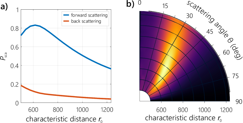
We produced a set of nearly Hud patterns with our modified RSA model and calculated the optical response using the corresponding structure factors and the form factor that was used throughout this work. For a characteristic distance of nm we find that at nm around 95% of the irradiating light hitting the interface undergoes scattering, of which the major part, , is scattered into the forward direction, see Figure 10a. In Figure 10b we plot the (forward direction) of these structures at the same wavelength.