Beatings of ratchet current magneto-oscillations in GaN-based grating gate structures: manifestation of spin-orbit band splitting.
Abstract
We report on the study of the magnetic ratchet effect in AlGaN/GaN heterostructures superimposed with lateral superlattice formed by dual-grating gate structure. We demonstrate that irradiation of the superlattice with terahertz beam results in the dc ratchet current, which shows giant magneto-oscillations in the regime of Shubnikov de Haas oscillations. The oscillations have the same period and are in phase with the resistivity oscillations. Remarkably, their amplitude is greatly enhanced as compared to the ratchet current at zero magnetic field, and the envelope of these oscillations exhibits large beatings as a function of the magnetic field. We demonstrate that the beatings are caused by the spin-orbit splitting of the conduction band. We develop a theory which gives a good qualitative explanation of all experimental observations and allows us to extract the spin-orbit splitting constant meVÅ. We also discuss how our results are modified by plasmonic effects and show that these effects become more pronounced with decreasing the period of the gating gate structures down to sub-microns.
I Introduction
One of the most important tasks of modern optoelectronics is to provide efficient conversion of high-frequency terahertz (THz) signals into a dc electrical response, for reviews see, e.g., Refs. [1, 2, 3, 4, 5, 6, 7, 8, 9]. In the last decades, the focus of research in this direction was on the periodic structures like field effect transistor (FET) arrays, grating gate, and multi-gate structures. Such structures also attract growing interest as simple examples of tunable plasmonic crystals [10, 11, 12, 13, 14]. Plasmonic crystals already demonstrated excellent performance as THz detectors [15, 16, 17, 18, 19, 20], in close agreement with the numerical simulations [21, 22, 23, 24, 25]. They are also actively studied as possible emitters or amplifiers of THz radiation [26, 27, 28].
Importantly, a non-zero dc photoresponse requires some asymmetry of the system, which would determine the direction of the produced dc current. Generation of dc electric current in response to ac electric field in systems with broken inversion symmetry is usually called the ratchet effect which was studied both theoretically and experimentally in a great number of systems, for reviews see, e.g., Refs. [29, 30, 31, 32, 33, 34]. For effective radiation conversion to dc signal in periodic structures, there should be strong built-in asymmetry inside the unit cell of the plasmonic crystals. In particular, the ratchet dc current can be induced by the electromagnetic wave incident on the spatially modulated system provided that the wave amplitude is also modulated but is phase-shifted in space, for review see Ref. [30]. On the theoretical level, the ratchet current arises already in non-interacting approximation (so called electronic ratchet). Electronic ratchets were discussed in the two dimensional systems with lateral gratings [30, 35, 36, 37, 38, 39, 40, 41] or arrays of asymmetric dots/antidots [42, 43, 44, 45]. Electron-electron (ee) interaction can dramatically increase ratchet current due to plasmonic effects [46, 47, 48, 49, 50, 51, 52, 53, 54].
Although the ratchet effect was treated theoretically and observed experimentally in diverse low dimensional spatially-modulated structures, some basic issues of this effect still remain puzzling. One of the interesting questions that has not yet been discussed in the literature is the manifestation of the effects of spin-orbit (SO) interaction in the ratchet effect. In this paper, we address this question. We study ratchet effect in magnetic field (in what follows, we call it magnetic ratchet effect) in the regime of Shubnikov de Haas (SdH) oscillations and demonstrate that it is dramatically modified by SO interaction. Specifically, we report on the observation of the magnetic ratchet effect in the lateral GaN-based superlattice formed by dual-grating gate (DGG) structure. The specific property of the GaN systems as compared to other 2D structures including graphene based structures is a very high value of Rashba spin-orbit coupling (at least ten times larger than in GaAs-based structures) [55, 56, 57, 58, 59, 60, 61, 62, 63], which is caused by high build-in electric field existing in such polar materials. This is, therefore, very favorable for observations of SO-induced effects. We demonstrate, both experimentally and theoretically, that in quantized magnetic fields THz excitation results in the giant magnetooscillations of the ratchet current coming from Landau quantization, which, due to large SO band splitting, are strongly modulated as a function of the magnetic field. We reach a good qualitative agreement between our experimental results and theory (compare, respectively, Fig. 6 and Fig. 7 below).
Our results provide a novel method to study the band spin splitting. Currently the most widely used techniques are direct measurements of magnetoresistance in SdH oscillations regime [64], the weak anti-localization experiments [65], optical methods [66] and photogalvanic studies [67]. Since SdH oscillations in magnetoresistance regime and ratchet current correlate, these two measuring methods are complementary, which gives the opportunity to double check the results.
The possibility to increase the ratchet effect in the magnetic field deserves special attention. Therefore, we start the paper with the discussion of the key points of the magnetic ratchet effect, see Sec. II. The rest of the paper is organized as follows. In Sec. III we present the experimental results on magnetic ratchet effects in GaN-based structures. In the following Sec. IV we present the theory and compare its results with the experimental data. Sec. IV.3 is devoted to the discussion of the plasmonic effects. Finally, in Sec. V we summarize the results.
II Ratchet effect in magnetic fields: state of the art
Physics of the ratchet effect becomes much richer if one applies the magnetic field. Magnetic ratchet effect, which is in some publications called magneto-photogalvanic effect, was widely studied in different semiconductor systems. The magnetic ratchet effect can be induced even in the case of homogeneous graphene with structure inversion asymmetry, see e.g. [68, 69, 70, 71, 72]. The effect is sensitive to disorder and can be tuned by the gate voltage [72]. Furthermore, the theoretical consideration of the magnetic ratchet effect in graphene and bi-layer graphene showed that it can be substantially enhanced under the cyclotron resonance (CR) condition [73]. Most recently it has been shown theoretically and observed experimentally that magnetic ratchet effect also can be drastically enhanced by deposition of asymmetric lateral potential introduced by asymmetric periodic metallic structure on top of a structure with two dimensional electron gas [74, 75, 76, 77]. Remarkably, magnetic ratchet strongly increases (by more than two orders of magnitude) in the SdH oscillations regime. Physically, this happens due to a very fast oscillations of the resistivity with the Fermi energy, and consequently, with the electron concentration. As a result, inhomogeneous (dynamical and static) density modulations induced by the electromagnetic wave leads to a very strong response.
Importantly, the responsivity in the regime of SdH oscillations increases not only in grating gate structures but also in single FETs [78, 79, 80, 81]. Although the general physics of enhancement in both cases is connected with fast oscillations of resistivity, there is an essential difference. In grating gate structures the shape of typical dc photoresponse roughly reproduces resistance oscillations, while in single FETs the typical response is shifted with respect to resistance oscillations. The latter shift was explained theoretically by hydrodynamic model in Ref. [79] and demonstrated experimentally in Ref. [81]. The key idea is as follows. Transport scattering rate in the SdH regime sharply depends on the dimensionless electron concentration (here is background concentration and is the concentration in the channel). Expanding with respect to small one finds that a nonlinear term, , appears in the Navier Stockes equation, where is the drift velocity. This is sufficient to give a nonzero response, which in a single FET arises in the second order with respect to external THz field (both and are linear with respect to this field). Therefore, in this case, the response is proportional to first derivative of with respect to concentration (i.e. with respect to Fermi energy, ), hence, it is shifted in respect to the conductivity oscillations. By contrast, in the grating gate structures, the dc response appears only in the third order with respect to perturbation [30]. As a consequence, the ratchet current is proportional to the second derivative (see discussion in Sec. IV) and therefore roughly (up to a smooth envelope) reproduces resistance oscillations.
We will show that similar to other structures [75, 74, 77], the amplitude of the magnetooscillations is greatly enhanced as compared to the ratchet effect at zero magnetic field. We experimentally demonstrate that the photocurrent oscillates in phase with the longitudinal resistance and, therefore, almost follows the SdH oscillations multiplied by a smooth envelope. This envelope encodes information about cyclotron and plasmonic resonances. The most important experimental result is the demonstration of the beatings of the ratchet current oscillations. We interpret these beatings assuming that they come from SO splitting of the conduction band. The value of SO splitting extracted from the comparison of the experiment and theory is in good agreement with independent measurements of SO band splitting [55, 56, 57, 58, 59, 60, 61, 62, 63].
An important comment should be made about the role of the ee interaction. Actually, the effect of the interaction is twofold. First of all, sufficiently fast ee collisions drive the system into the hydrodynamic regime. We assume that this is the case for our system and use the hydrodynamic approach. Secondly, ee-interaction leads to plasmonic oscillations, so that a new frequency scale, the plasma frequency, appears in the problem, where is the inverse characteristic of the spatial scale in the system. For a device with a short length, for example, for a single FET, is proportional to the inverse length of the device. For periodic grating gate structures, where is the period of the structure. At zero magnetic field, the dc response is dramatically enhanced in the vicinity of plasmonic resonance, both for a single FET with asymmetric boundary conditions [82] and for periodic asymmetric grating gate structures [54]. Also, the response essentially depends on the polarization of the radiation.
Here, we calculate analytically the dc response in the quantizing magnetic field within the hydrodynamic approximation for arbitrary polarization of the radiation and analyzed plasmonic effects. One of our main prediction is that for linearly polarized radiation, the dependence of the ratchet current on the direction of the polarization appears only due to the plasmonic effects. We use the derived expression to prove that for specific parameters of our structures the plasmonic effects are negligible, and as a consequence, the dc response does not depend on the polarization direction. The latter issue is very important for us since the direction of linear polarization used in our experiment was not well controlled. We also argue how to modify the structures in order to observe plasmonic resonances.
III Experiment
III.1 Experimental details
We choose AlGaN/GaN heterostructure system for the experimental study of the effect of SO splitting on magnetic ratchet effect. Important unique properties of GaN system are the ability to form high density, high mobility two dimensional electron gas (2DEG) on the AlGaN/GaN interface, and large Rashba spin splitting of the conduction band [55, 56, 57, 58, 59, 60, 61, 62, 63]. Density of 2DEG and the band spin splitting in this system are about an order of magnitude higher than that in AlGaAs/GaAs system. High carrier density is an important factor because as will be shown later the amplitude of the photoresponse in the regime of the SdH oscillations is proportional to the square of electron density.
AlGaN/GaN heterostructures were grown by Metalorganic Vapour Phase Epitaxy (MOVPE) method in the closed coupled showerhead inch Aixtron reactor (Aixtron, Herzogenrath, Germany). The epi-structure consisted of 25 nm barrier layer, 1.5 nm spacer, 0.9 m unintentionally doped (UID) GaN layers, and 2 m high resistive GaN:C buffer, see Fig. 1(a). Growth of all mentioned epilayers was done on the bulk semi-insulating GaN substrates, grown by the ammonothermal method [83]. In this method high resistivity of substrates (typically no less than ) was obtained by compensation of residual oxygen, incorporated during ammonothermal growth, by Mg shallow acceptors.
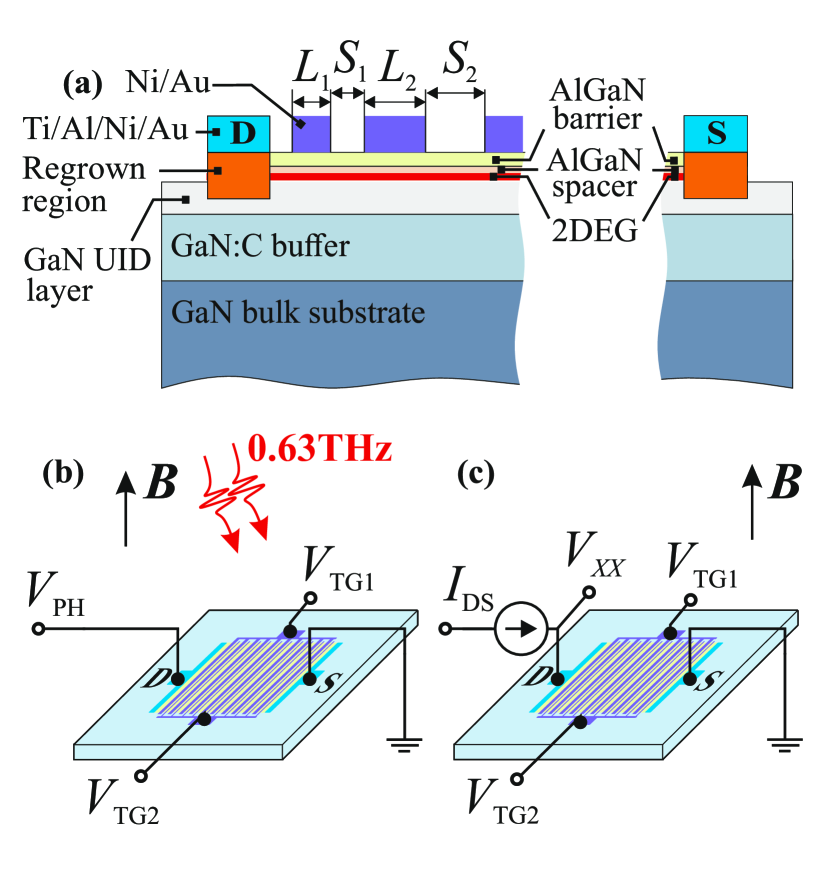
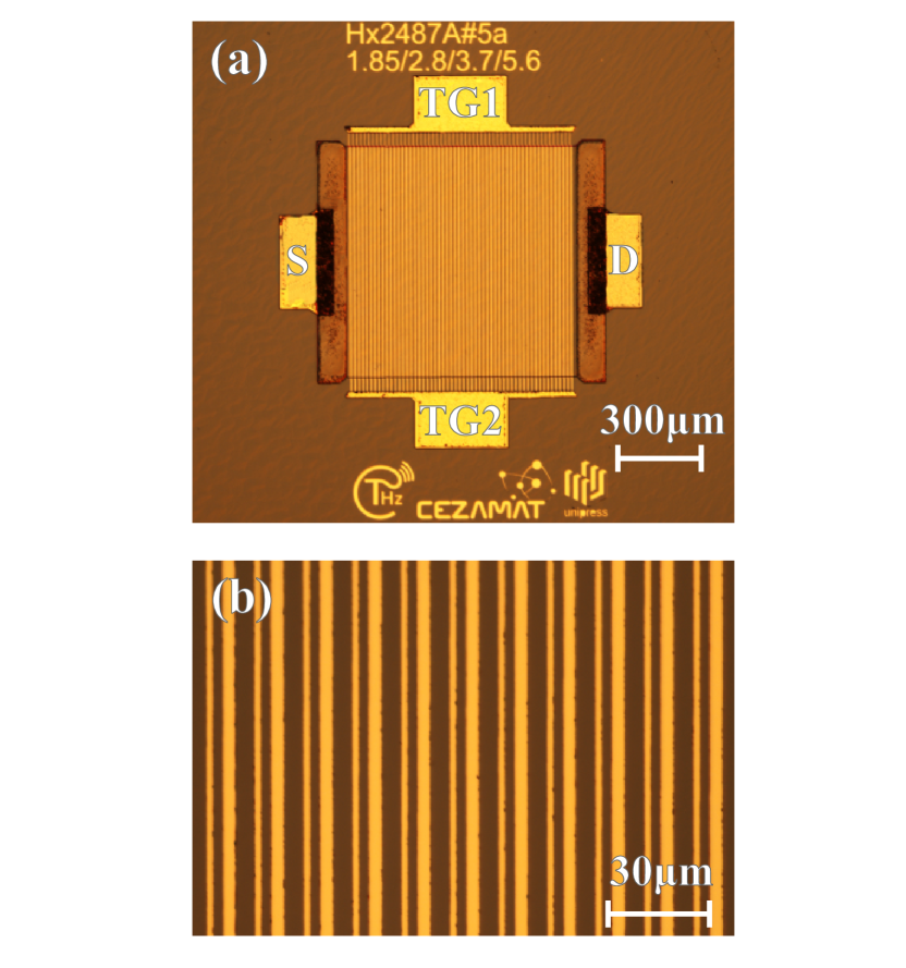
The structures lithography processing was performed using a commercial 405 nm laser writer system (Microtech, Palermo, Italy). Devices were isolated from each other by shallow 150 nm mesas etched by Inductively Coupled Plasma – Reactive Ion Etching (ICP-RIE) (Oxford Instruments, Bristol, UK). In order to form the drain and source ohmic contacts Ti/Al/Ni/Au (150/1000/400/500 Å) stacks were deposited on the MOVPE regrown heavily doped sub-contact regions (for the detailed information of the regrowth technique see Ref. [84]). Source and drain contacts, see Fig. 1, were annealed at 780 C∘ in a nitrogen atmosphere for 60 s. This procedure yielded reproducible ohmic contacts with resistances in the range of -. Finishing fabrication step was the deposition of Ni/Au (100/300 Å) in order to form the DGG superlattice on the top of the AlGaN/GaN mesas. A schematic view and Nomarski contrast microscope photos of fabricated devices are shown in Figs. 1(a) and 2, respectively. The unit cell of the DGG superlattice consisted of two gates of different lengths (m and m) with different spacings between them (m and m). The cell was repeated 35 times resulting in a superlattice with a total length of 500 m.
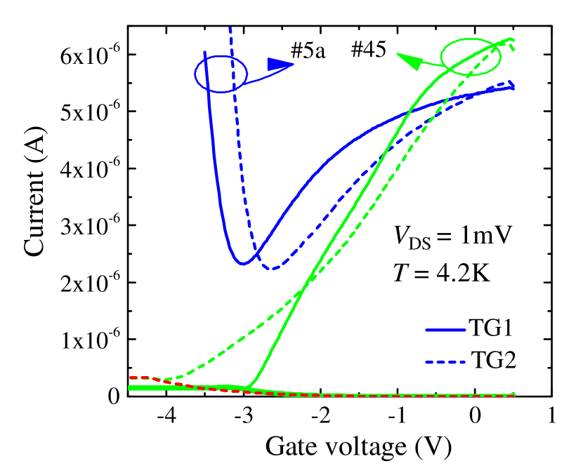
All wide gates were connected forming the multi-finger top gate electrode TG1, see Fig. 1(b,c) and Fig. 2(a). Similarly connected narrow gates formed the gate electrode TG2. Independent bias voltages () could be applied to wide and narrow gates. The width of the whole structure was 0.5 mm yielding the total active area mm2. The total gate area was . This is a large area, which is 4 orders of magnitude bigger than that for the ”standard” transistor with gate length and width of 0.1 m and 100 m, respectively. This made very challenging the fabrication of the described DGG transistor with a reasonably small gate leakage current. Figure 3 shows two examples of the transfer current voltage characteristics of the studied devices. Current in the subthreshold region is determined by the gate leakage current (shown as a red dashed line for one of the devices). As seen, the gate leakage current is rather small, significantly smaller than the drain current even at a very low drain voltage of mV. Even for those devices with relatively high gate leakage current (5 in Fig. 3) the drain current and, therefore electron concentration can be changed several times by the gate voltage.
Experimental set up is shown in Figs. 1(b) and (c). As a radiation source a frequency multiplier from Virginia Diodes Inc. with a radiation frequency of =630 GHz was used to study the ratchet effect. The radiation was guided onto the sample through a steel waveguide and was modulated at a frequency of about 173 Hz. External magnetic field up to 12 T was applied normally to 2DEG plane, as shown in Fig. 1(b). The photoresponse, , was measured in a cryostat at the temperature of 4.2 K in the open circuit configuration using the standard lock-in technique. Magnetoresistance was measured by applying a small A current to the drain (see Fig. 1c).

III.2 Experimental results
First, we describe the results of the magnetotransport measurements, which are summarized in Figs. 4, and 5. The overall shape of the DGG structures was close to the square. Therefore, in the magnetic field perpendicular to the drain to source plane investigated structures exhibited geometrical magnetoresistance [85]. The full geometrical magnetoresistance is observed either in the disk Corbino geometry or in the samples with . For the arbitrary shaped rectangular samples, the geometrical magneto resistance can be approximated as [86]:
| (1) |
This allowed us to extract the electron mobility. Figure 4 shows the experimental dependence of the magnetoresistance obtained for a weak magnetic field for one of the samples as a function of . The estimate yields cm2/Vs.
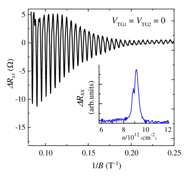
The concentration in the channel can be extracted from the magneto resistance in the higher magnetic fields. Figure 5 shows the resistance SdH oscillations as a function of the inverse magnetic field measured for both top gate voltages equal to zero. The concentration is given by
| (2) |
where and are the period and frequency of SdH oscillations, respectively. The inset in Fig. 5 shows the result of the Fourier transform of the resistance magnetooscillations with the frequency taken in the units of the electron concentration, . Two peaks in the inset correspond to the concentrations cm-2 and cm-2, which we interpret as electron densities in the gate free and under the gate areas, respectively.
Irradiating the unbiased structures we detected a photosignal caused by the generation of the ratchet photocurrent. Figure 6(a) shows the photoresponse measured for asymmetric gate voltages applied: . The photoresponse current was calculated as . In low and zero magnetic fields the response is positive and weakly depends on the magnetic field. When gate voltages were changed to the magnitude of the response was approximately the same, but of the negative sign. The change of the signal sign upon inversion of the lateral asymmetry is a clear indication that the observed photocurrent is caused by the ratchet effect, for review see Ref. [30]. Indeed, the direction of the current is controlled by the lateral asymmetry parameter [30]
| (3) |
where and are spatially modulated by grating gates static potential and electric field amplitude (over-line shows average over the modulation period). Exchange of the gate voltages applied to the TG1 and TG2 results in the change of sign of and, consequently in the sign inversion of the ratchet current.
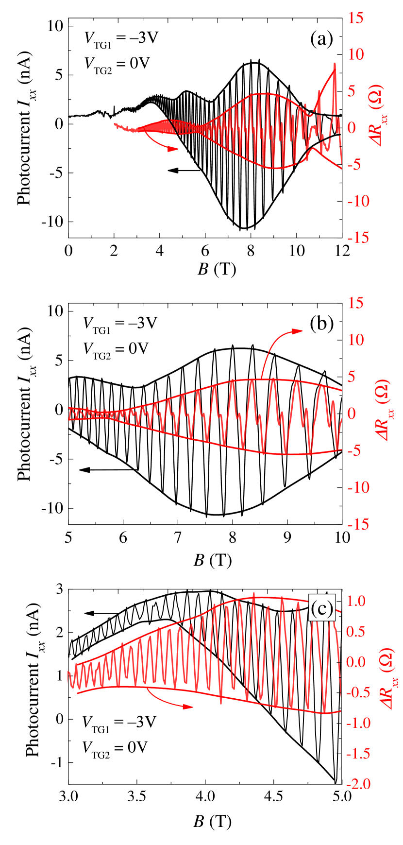
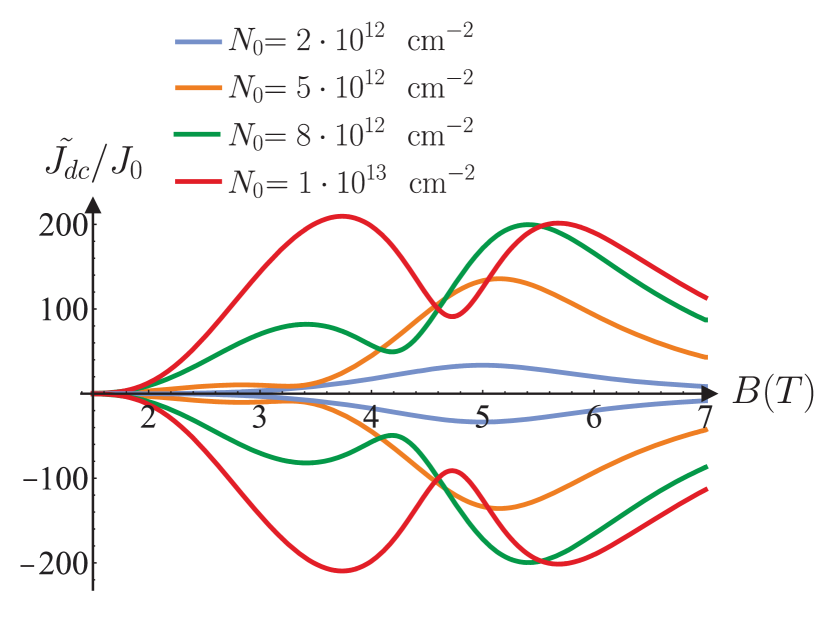
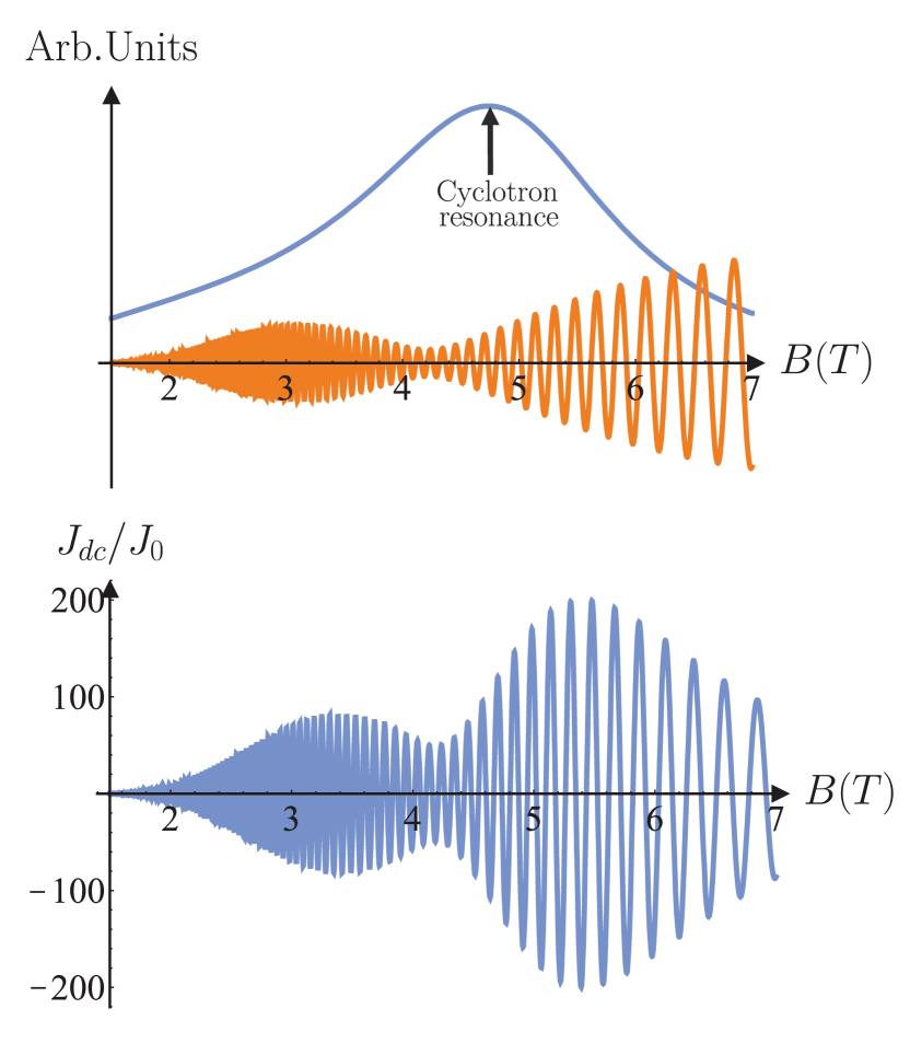
The increase of magnetic field results in the sign-alternating oscillations with the amplitude by orders of amplitude larger than the signal obtained for zero magnetic field. Moreover, the envelope of the oscillations exhibits large beatings as a function of magnetic field. Comparison of the observed oscillations with the SdH magnetoresistance oscillations demonstrates that at high magnetic fields both, photocurrent and resistivity oscillations, have the same period and phase. Importantly, SdH effect also show similar beatings of the envelope function. To facilitate the comparison of the phase of the oscillations, we zoom the data of the panel (a) for the range of fields T in the panel (b) Fig. 6.
The overall behavior of the observed current, besides beatings, corresponds to that of the magneto-ratchet current most recently detected in CdTe-based quantum wells [74, 75] and graphene [77]. Importantly, the oscillations of the magneto-ratchet current are in phase with the SdH oscillations. As we discussed in Sec. II, this differs from the photocurrent magnetooscillations detected in single transistors [81] described by the theoretical model of Lifshits and Dyakonov [79]. We will show in Sec. IV that the theory of the magneto-ratchet effect predicts the photoresponse to be proportional to the second derivative of the magnetoresistance, and, hence describes well the experimental findings. Note, that in the low magnetic field range, see Fig. 6(c), the oscillations of the photoresponse and magnetoresistance are phase shifted. This is an indication that at low magnetic fields we have at least two different competing mechanisms of the detection. Below we focus on the case of sufficiently high magnetic fields and postpone discussion of possible competing mechanisms at low fields for future research. Importantly, the theory demonstrates that, in agreement with the experiment (see Fig. 6) the photoresponse in the regime of SdH oscillations is significantly enhanced as compared to that at zero magnetic field. This point is very important in view of possible applications and deserves a special comment. The theoretical limit for the response of the detectors based on the direct rectification is defined by the device built-in nonlinearity. In Schottky diodes and FETs the maximum current responsivity is approximately , where is the elemental charge and is the ideality factor of the Schottky barrier or subthreshold slope of FET transfer characteristic [87, 88]. The responsivity of the real device is usually orders of magnitude smaller due to the parasitic elements and not perfect coupling. However, increasing of the theoretical limit still should be beneficial for the increasing of the responsivity in real devices. Reducing temperature indeed leads to the responsivity increase but only to a certain limit. As shown in [89] the temperature decrease below 30K does not lead to the increase of responsivity. This low-temperature saturation is caused by the increase of factor with temperature decrease which is known in Schottky diodes and FETs [90]. In the magnetic field under the regime of SdH oscillations resistance of FET very sharply depends on the gate voltage and provides the opportunity to go beyond limit. We can speculate that about an order of magnitude increase of the responsivity in an external magnetic field in Fig. 6 demonstrates the increase of the physical responsivity beyond the fundamental limit.
Importantly, the theory presented below also describes well the observed oscillations of the envelope amplitude of the photoresponse, which are clearly seen in Fig. 6. It shows that the oscillations are due to the spin-splitting of the conduction band and can be used to extract this important parameter.
IV Theory
Above, we experimentally demonstrated that the photocurrent oscillates and the shape of these oscillations almost follow the SdH resistivity oscillations. In this section, we consider gated 2DEG and demonstrate that the results can be well explained within the hydrodynamic approach.
The effect which we discuss here is present for the system with an arbitrary energy spectrum. However, calculations are dramatically simplified for the parabolic spectrum, so that we limit calculations to this case only. We assume that electron density in the structure is periodically modulated by built-in static potential and study optical dc response to linearly-polarized electromagnetic radiation which is also spatially modulated with the phase shift with respect to modulation of the static potential.
A variation of individual gate voltages of the DGG lateral structure allows one to change controllably the sign of and, consequently, the direction of the ratchet current. Furthermore, the phase of the oscillations of the magnetic ratchet current is sensitive to the orientation of the radiation electric field vector with respect to the DGG structure as well as to the radiation helicity. In the latter case, switching from right- to left-circularly polarization results in the phase shift by , i.e., at constant magnetic field the helicity-dependent contribution to the current changes the sign. We consider magnetic field induced modification of the zero -field electronic ratchet effect. We also analyze our results theoretically for different relation between and having in mind to find signature of the plasmonic effects.
IV.1 Model
We model electric field of the radiation, and the static potential, as follows
| (4) | ||||
| (5) | ||||
| (6) |
where is the modulation depth, is the phase, which determines the asymmetry of the modulation, and are constant phases describing the polarization of the radiation. These phases are connected with the standard Stockes parameters (normalized by ) as follows:
| (7) | ||||
Within this model, asymmetry parameter [see Eq. (3)] becomes
| (8) |
As seen, is proportional to the sine of the spatial phase shift
Hydrodynamic equations for concentration and velocity look
| (9) | ||||
| (10) |
Here
| (11) |
is the concentration in the channel and its equilibrium value,
| (12) |
is the cyclotron frequency in the external magnetic field , is the plasma waves velocity, is momentum relaxation rate. The non-linearity is encoded in hydrodynamic terms as well as independence of transport scattering rate on the concentration. Specifically, we use the approach suggested in Ref. [79]. We assume that is controlled by the local value of the electron concentration, which, in turn, is determined by the local value of the Fermi energy, (here we took into account that the 2D density of states is energy-independent). Due to the SdH oscillations, scattering rate is an oscillating function of and, consequently, oscillates with In the absence of SO coupling, is given by [79]
| (13) |
where
| (14) |
is the amplitude of the SdH oscillations,
is the temperature in the energy units, is the local Fermi energy, which is related to concentration in the channel as (here is the density of states), and is quantum scattering time, which can be strongly renormalized by electron-electron collisions in the hydrodynamic regime. We assume that Then,
| (15) |
and the second term in the curly brackets in Eq. (13) is very small. Hence is very close to the value of transport scattering rate at zero magnetic field.
Eq. (13) can be generalized for the case of non-zero SO coupling by using results of Refs. [75, 91, 92]
| (16) | |||
Here we assumed that there is linear-in-momentum spin-orbit splitting of the spectrum, where
| (17) |
is characterized by coupling constant Experimentally measured values of lays between 4-10 meVÅ [55, 56, 57, 58, 59, 60, 61, 62, 63]. For such values of and typical values of the concentration, one can assume and neglect dependence of on . Equation (16) was derived under the assumption that the quantum scattering time is the same in two spin-orbit split subbands. Actually, this assumption is correct only for the model of short range scattering potential where both transport and quantum scattering rates are momentum independent. For any finite-range potential, the quantum scattering times in two subbands differ, because of small difference of the Fermi wavevectors and Denoting these times as and we get instead of Eq. (16):
| (18) |
where
| (19) |
Detailed microscopical calculation of for specific model of the scattering potential is out of the scope of the current work. Here, we use as fitting parameters.
Let us now expand near the Fermi level:
| (20) |
where and are, respectively, first and second derivatives with respect to taken at the Fermi level. Since oscillations are very fast, we assume
| (21) |
Due to these inequalities oscillating contribution to the ratchet current can be very large and substantially exceed zero-field value [77].
Here, we focus on SdH oscillations of the ratchet current, so that we only keep oscillations related to dependence of on and, moreover, skip in Eq. (20) the term proportional to
IV.2 Calculations and results
Let us formulate the key steps of calculations. Due to the large parameter, the main contribution to the rectified ratchet current comes from the non-linear term in the r.h.s. of Eq. (10) [see also Eq. (20)]. We, therefore, neglect all other nonlinear terms in the hydrodynamic equations. Calculating and in linear (with respect to and ) approximation, substituting the result into non-linear term and averaging over time and coordinate, we get Next, one can find rectified current by averaging of Eq. (10) over and . This procedure is quite standard, so that we delegate it to the Supplemental Material (similar calculations were performed in Ref. [54] for zero magnetic field). The result reads
| (23) |
Here
| (24) |
is the frequency and magnetic field independent parameter with dimension of the current (physically, gives the typical value of current for the case,when all frequencies are of the same order, ), the dimensionless factor accounts for SdH oscillations and dimensionless vector
| (25) |
depends on the radiation polarization encoded in the vectors
() and also contains information about cyclotron and magnetoplasmon resonances which occur for and respectively. The latter resonance appears due to the factor in the denominator of Eq. (25). Analytical expressions for and are quite cumbersome and presented in the Supplementary material [see Eqs. (49), (55), (58), (61) and (65)].
The second derivative of the scattering rate with respect to is calculated by using Eq. (18):
| (26) | ||||
Here, [see Eq. (19)]. The function rapidly oscillates due to the factors For this function goes to zero due to the Dingle factors so that discussed mechanism has nothing to do with the zero field ratchet effect.
The smooth envelope of the function reads
| (27) | ||||
Function shows rapid SdH oscillations with the beats due to the spin orbit coupling. As seen from the behavior of the envelope function the beats are most pronounced for when is proportional to and therefore vanishes at the values of obeying For envelope function is nonzero at these points, and beats are less pronounced.
Now, we are ready to explain why the response in the SdH oscillation regime is much larger than at zero magnetic field. The enhancement of the response as compared to the case is due to the factor
| (28) |
One can check that for experimental values of parameters inequalities Eq. (15) and (28) are satisfied simultaneously in a wide interval of magnetic fields, T. It is also important that due to the coefficient in the the response increases with the concentration in contrast to conventional transistor operating at where response is inversely proportional to the concentration at high concentration [82] and saturates at low concentration when a transistor is driven below the threshold [93]. This means that the use of AlGaN/GaN system for detectors operating in the SdH oscillation regime is very advantageous because of the extremely high concentration of 2DEG.
Let us discuss the polarization dependence of the response. Importantly, vectors responsible for polarization dependence, contain -independent terms and terms proportional to The latter describe plasmonic effects. As seen from Eqs. (49),(55), (58), for small (or/and small ), vectors and are small, In other words, for our case of linearly-polarized radiation with polarization directed by angle the dependence of the rectified current on appears only due to the plasmonic effects. For experimental values of the parameters, the value of plasmonic frequency, was sufficiently small, about s which is much smaller than the radiation frequency (for THz we get s-1). As follows from this estimate, the plasmonic effects are actually small and can be neglected.
Then, the response does not actually depend on polarization angle This justifies our experimental approach, where is not well controlled. Within this approximation, one can put in Eqs. (49),(55), (58), and (65). Then, the analytical expression for current simplifies. In the absence of the circular component of polarization (), we get
| (29) |
This expression simplifies even further in the resonant regime, :
| (30) |
This expression shows rapid oscillations, described by function which envelope represent a sharp CR with the width
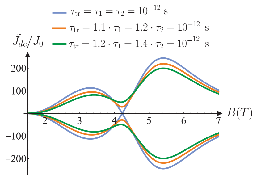
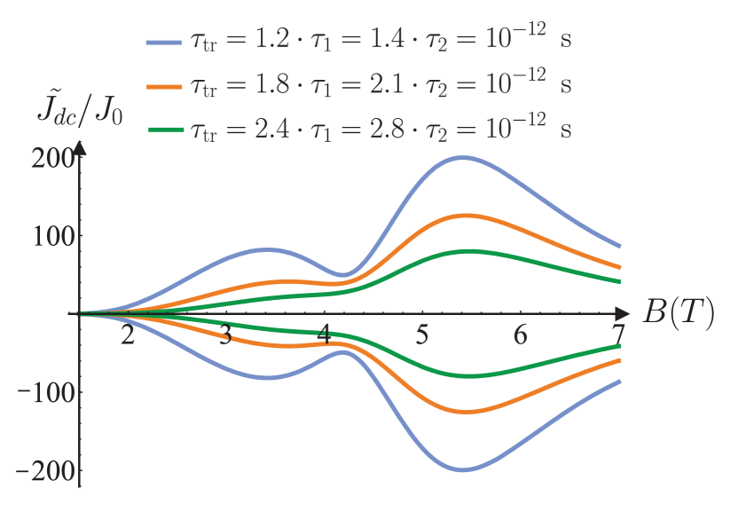
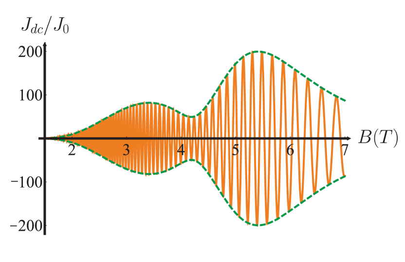
Let us now compare theoretical results with experimental observations. In Fig. 7 we plot the component of the rectified dc current (this component was actually measured in the experiment), calculated with the use of Eq. (23), as a function of the magnetic field. We assumed that the radiation is linearly-polarized along axis [, see Eqs. (4),(5), and (7)] and used experimental values of parameters: cm, cm, K, cms, s-1. The best fit was obtained for meVÅ, in accordance with previous measurements of SO band splitting [55, 56, 57, 58, 59, 60, 61, 62, 63]. We used as the fitting parameters choosing We see that exactly this behavior is observed in the experiment (see Fig. 6). Most importantly, we reproduce experimentally observed beats of SdH oscillations using the value of consistent with previous experiments. In Figs. 8, 10, and 9 we show dependence of the smooth envelope of the current, on magnetic field for different values of and different concentrations. As we explained above, the most pronounced modulation is obtained for (see Fig. 8). Dependence on concentration appears both due to the factor in and due to the dependence of on
IV.3 Role of the plasmonic effects
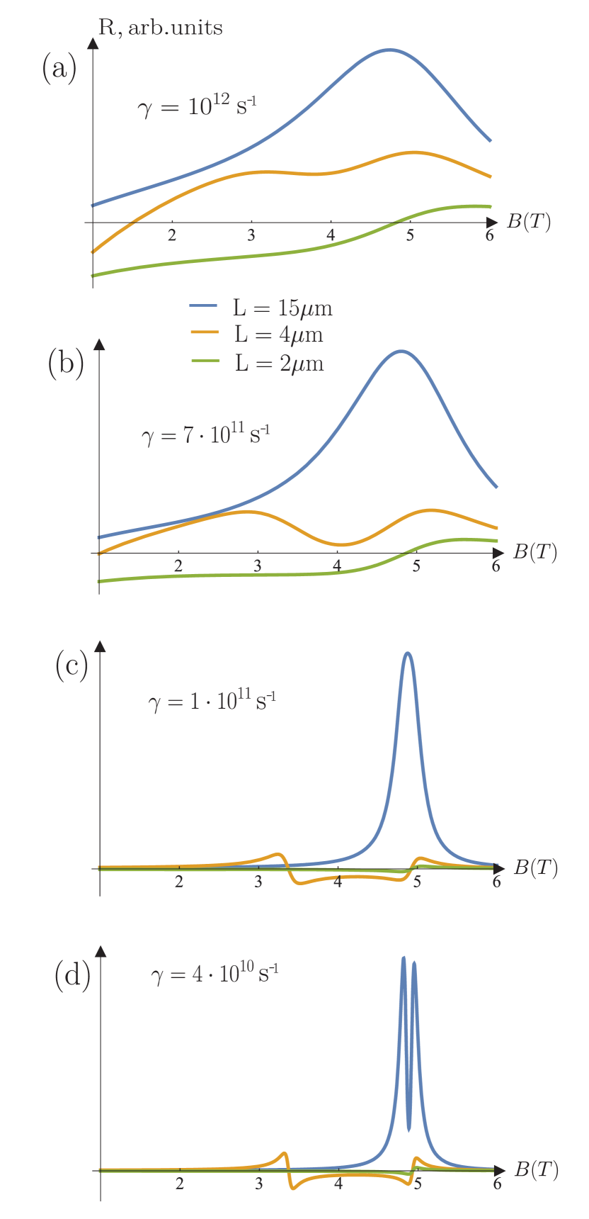
Above, we demonstrated that plasmonic effects can be neglected for our experimental parameters and, as a consequence, the response is insensitive to the direction of the linear polarization. However, the role of plasmonic effects is not fully understood. The point is that the existing ratchet theory assumes a weak coupling with a diffraction grating. In such a situation, the plasmon wave vector, which determines plasma oscillations frequency, is set by the total lattice period: . In the experiment, = 13.95 m, i.e. is very large and, as a consequence, the plasma frequency corresponding to the full period is small. This frequency does not appear in the experiment, as follows from the theoretical pictures presented above (see Fig. 12a). If we assume, that the coupling is not so weak, then the plasmons determined only by the gate region, should show up. Then is determined only by the gate length and it should manifest itself, as it is shown in Fig. 12. Namely, plasma wave effects should lead to the plasmonic splitting of the CR.
The role of the plasmonic effects can be enhanced either by decreasing the period of the structure, which implies increasing of or by decreasing transport scattering rate as illustrated in Fig. 12, where cyclotron and magnetoplasmon resonances in the smooth function [see Eq. (25)] are shown for different values of and Although, for large values of (Fig. 12a) plasmonic effects are fully negligible for small (large ) and function shows only CR at with decreasing there appears a week plasmonic resonance at For smaller (Fig. 12 b, c), both cyclotron and magnetoplasmonic resonances become sharper. For very small (Fig. 12c), plasmonic resonance appears even for very small
V Conclusion
To conclude, we presented observation of the magnetic ratchet effect in GaN-based structure superimposed with lateral superlattice formed by dual-grating gate (DGG) structure. We showed that THz excitation results in the giant magnetooscillation of the ratchet current in the regime of SdH oscillations. The amplitude of the oscillations is greatly enhanced as compared to the ratchet effect at zero magnetic field. We demonstrate that the photocurrent oscillates as the second derivative of the longitudinal resistance and, therefore, almost follow the SdH resistivity oscillations multiplied by a smooth envelope. This envelope encodes information about cyclotron resonance. One of the most important experimental results is the demonstration of beats of the ratchet current oscillations. We interpret these beats theoretically assuming that they come from SO splitting of the conduction band. The value of SO splitting extracted from the comparison of the experiment and theory is in good agreement with independent measurements of SO band splitting. We also discuss conditions required for the observation of magnetoplasmon resonances.
VI Acknowledgements
A financial support of the IRAP Programme of the Foundation for Polish Science (grant MAB/2018/9, project CENTERA) is greatfully acknowledge. The partial support by the National Science Centre, Poland allocated on the basis of Grant Nos. 2016/22/E/ST7/00526, 2019/35/N/ST7/00203 and NCBIR WPC/20/DefeGaN/2018 is acknowledged. S.D.G. thanks DFG-RFBR project (numbers Ga501/18-1 and 21-52-12015) and Volkswagen Stiftung Cooperation Program (97738). The work of S.P. and V.K. was funded by RFBR, project numbers 20-02-00490 and 21-52-12015, and by Foundation for the Advancement of Theoretical Physics and Mathematics.
References
- [1] S. A. Maier, Plasmonics: Fundamentals and Applications (Springer, 2007).
- [2] D. K. Gramotnev, S. I. Bozhevolnyi, Nature Photonics 4, 83 (2010).
- [3] F. H. L. Koppens, D. E. Chang, F. Javier Garcia de Abajo, Nano Lett. 11, 3370 (2011).
- [4] Joerg Heber, Nature Materials 11, 745 (2012).
- [5] A. N. Grigorenko, M. Polini, K. S. Novoselov, Nature Photonics 6, 749 (2012).
- [6] Peter Nordlander, Nature Nanotechnology 8, 76 (2013).
- [7] M. Glazov and S. Ganichev, Phys. Rep. 535, 101 (2014).
- [8] Koppens, F. H. L.; Mueller, T.; Avouris, P.; Ferrari, A. C.; Vitiello, M. S.; Polini, M. Nature Nanotechnology 9, 780 (2014).
- [9] Jacob B. Khurgin, Nature Nanotechnology 10, 2 (2015).
- [10] G. C. Dyer, G. R. Aizin, S. Preu, N. Q. Vinh, S. J. Allen, J. L. Reno, and E. A. Shaner, Phys. Rev. Lett. 109, 126803 (2012).
- [11] G. R. Aizin, G. C. Dyer, Phys. Rev. B 86 235316 (2012).
- [12] V. Yu. Kachorovskii and M. S. Shur, Appl. Phys. Lett. 100, 232108 (2012).
- [13] Gregory C. Dyer, Gregory R. Aizin, S. James Allen, Albert D. Grine, Don Bethke, John L. Reno, and Eric A. Shaner, Nature Photonics 7, 925 (2013).
- [14] Lin Wang, Xiaoshuang Chen, Weida Hu1, Anqi Yu, and Wei Lu, Appl. Phys. Lett. 102, 243507 (2013).
- [15] X. G. Peralta, S. J. Allen, M. C. Wanke, N. E. Harff, J. A. Simmons, M. P. Lilly, J. L. Reno, P. J. Burke, and J. P. Eisenstein, Appl. Phys. Lett. 81, 1627 (2002).
- [16] E. A. Shaner, Mark Lee, M. C. Wanke, A. D. Grine, J. L. Reno, and S. J. Allen, Appl. Phys. Lett. 87, 193507 (2005).
- [17] E. A. Shaner, M. C. Wanke, A. D. Grine, S. K. Lyo, J. L. Reno, and S. J. Allen, Appl. Phys. Lett. 90, 181127 (2007).
- [18] A. V. Muravjov, D. B. Veksler, V. V. Popov, O. V. Polischuk, N. Pala, X. Hu, R. Gaska, H. Saxena, R. E. Peale, and M. S. Shur, Appl. Phys. Lett. 96, 042105 (2010).
- [19] G. C. Dyer, S. Preu, G. R. Aizin, J. Mikalopas, A. D. Grine, J. L. Reno, J. M. Hensley, N. Q. Vinh, A. C. Gossard, M. S. Sherwin, S. J. Allen, and E. A. Shaner , Appl. Phys. Lett., 100, 083506 (2012).
- [20] X. Cai, A. B. Sushkov, R. J. Suess, M. M. Jadidi, G. S. Jenkins, L. O. Nyakiti, R. L. Myers-Ward, S. Li, J. Yan, D. K. Gaskill, T. E. Murphy, H. D. Drew, and M. S. Fuhrer, Nat. Nanotechnol. 9, 814 (2014).
- [21] G. R. Aizin, V. V. Popov, and O. V. Polischuk Appl. Phys. Lett. 89, 143512 (2006).
- [22] G. R. Aizin, D. V. Fateev, G. M. Tsymbalov, and V. V. Popov Appl. Phys. Lett. 91, 163507 (2007).
- [23] T. V. Teperik, F. J. Garci’a de Abajo, V. V. Popov, and M. S. Shur Appl. Phys. Lett. 90, 251910 (2007).
- [24] V. V. Popov, D. V. Fateev, T. Otsuji, Y. M. Meziani, D. Coquillat, and W. Knap, Appl. Phys. Lett. 99, 243504 (2011).
- [25] V. V. Popov, D. V. Fateev, E. L. Ivchenko, and S. D. Ganichev. Phys. Rev. B, 91, 235436 (2015).
- [26] Y. M. Meziani, H. Handa, W. Knap, T. Otsuji, E. Sano, V. V. Popov, G. M. Tsymbalov, D. Coquillat, and F. Teppe Appl. Phys. Lett. 92, 201108 (2008).
- [27] T. Otsuji, Y. M. Meziani, T. Nishimura, T. Suemitsu, W. Knap, E. Sano, T. Asano, and V. V. Popov, J. Phys.: Condens. Matter 20, 384206 (2008).
- [28] S. Boubanga-Tombet, W. Knap, D. Yadav, A. Satou, D. B. But, V. V. Popov, I. V. Gorbenko, V. Kachorovskii, and T. Otsuji, Phys. Rev. X 10, 031004 (2020).
- [29] P. Reimann, Phys. Rep. 361, 57 (2002).
- [30] E.L. Ivchenko and S. D. Ganichev, Pisma v ZheTF 93, 752 (2011) [JETP Lett. 93, 673 (2011)].
- [31] P. Hanggi and F. Marchesoni, Rev. Mod. Phys. 81, 387 (2009).
- [32] S. Denisov, S. Flach, and P. Hänggi, Phys. Rep. 538, 77 (2014).
- [33] D. Bercioux and P. Lucignano, Rep. Prog. Phys. 78, 106001 (2015).
- [34] C. O. Reichhardt and C. Reichhardt, Annu. Rev. Con-dens. Matter Phys. 8, 51 (2017).
- [35] P. Olbrich, E. L. Ivchenko, R. Ravash, T. Feil, S. D. Danilov, J. Allerdings, D. Weiss, D. Schuh, W. Wegscheider, and S. D. Ganichev, Phys. Rev. Lett. 103, 090603 (2009).
- [36] Yu.Yu. Kiselev and L.E. Golub, Phys. Rev. B 84, 235440 (2011).
- [37] P. Olbrich, J. Karch, E. L. Ivchenko, J. Kamann, B. März, M. Fehrenbacher, D. Weiss, and S. D. Ganichev, Phys. Rev. B 83, 165320 (2011).
- [38] A. V. Nalitov, L. E. Golub, E. L. Ivchenko, Phys. Rev. B 86, 115301 (2012).
- [39] G. V. Budkin and L. E. Golub, Phys. Rev. B 90, 125316 (2014).
- [40] P. Olbrich, J. Kamann, M. König, J. Munzert, L. Tutsch, J. Eroms, D. Weiss, Ming-Hao Liu, L. E. Golub, E. L. Ivchenko, V. V. Popov, D. V. Fateev, K. V. Mashinsky, F. Fromm, Th. Seyller, and S. D. Ganichev, Phys. Rev. B, 93, 075422 (2016).
- [41] S. D. Ganichev, D. Weiss, and J. Eroms, Ann. Phys. 529, 1600406 (2018).
- [42] A. D. Chepelianskii, M. V. Entin, L. I. Magarill, and D. L. Shepelyansky, Phys. Rev. E 78, 041127 (2008).
- [43] S. Sassine, Yu. Krupko, J.-C. Portal, Z.D. Kvon, R. Murali, K.P. Martin, G. Hill, and A.D. Wieck, Phys. Rev. B 78, 045431 (2008).
- [44] L. Ermann and D. L. Shepelyansky, Eur. Phys. J. B 79, 357 (2011).
- [45] E.S. Kannan, I. Bisotto, J.-C. Portal, T. J. Beck, and L. Jalabert, Appl. Phys. Lett. 101, 143504 (2012).
- [46] V. V. Popov, D. V. Fateev, T. Otsuji, Y. M. Meziani, D. Coquillat, and W. Knap, Appl. Phys. Lett. 99, 243504 (2011).
- [47] V. V. Popov, Appl. Phys. Lett. 102, 253504 (2013).
- [48] T. Otsuji, T. Watanabe, S. A. B. Tombet, A. Satou, W. M. Knap, V. V. Popov, M. Ryzhii, and V. Ryzhii, IEEE Trans. Terahertz Sci. Technol. 3, 63 (2013).
- [49] T. Watanabe, S. A. Boubanga-Tombet, Y. Tanimoto, D. Fateev, V. Popov, D. Coquillat, W. Knap, Y.M. Meziani, Yuye Wang, H. Minamide, H. Ito, and T. Otsuji, IEEE Sensors J. 3, 89 (2013).
- [50] Y. Kurita, G. Ducournau, D. Coquillat, A. Satou1, K. Kobayashi, S. Boubanga Tombet, Y. M. Meziani, V. V. Popov, W. Knap, T. Suemitsu, and T. Otsuji, Appl. Phys. Lett. 104, 251114 (2014).
- [51] S. A. Boubanga-Tombet, Y. Tanimoto, A. Satou, T. Suemitsu, Y. Wang, H. Minamide, H. Ito, D. V. Fateev, V. V. Popov, and T. Otsuji, Appl. Phys. Lett. 104, 262104 (2014).
- [52] L. Wang, X. Chen, and W. Lu, Nanotechnology 27, 035205 (2015).
- [53] P. Faltermeier, P. Olbrich, W. Probst, L. Schell, T. Watanabe, S. A. Boubanga-Tombet, T. Otsuji, and S. D. Ganichev, J. Appl. Phys. 118, 084301 (2015).
- [54] I.V. Rozhansky, V.Yu. Kachorovskii, and M.S. Shur, Phys. Rev. Lett. 114, 246601 (2015).
- [55] W. Weber, S.D. Ganichev, Z.D. Kvon, V.V. Bel’kov, L.E. Golub, S.N. Danilov, D. Weiss, W. Prettl, Hyun-Ick Cho, and Jung-Hee Lee, Appl. Phys. Lett. 87, 262106 (2005).
- [56] Ç Kurdak, N. Biyikli, Ü Özgür, H. Morkoç, and V. I. Litvinov, Phys. Rev. B, 74 113308 (2006).
- [57] A. N. Thillosen, Th. Schäpers, N. Kaluza, H. Hardtdegen, and V. A. Guzenko, Appl. Phys. Lett. 88, 022111 (2006).
- [58] S. Schmult, M. J. Manfra, A. Punnoose, A. M. Sergent, K. W. Baldwin, and R. J. Molnar, Phys. Rev. B 74, 033302 (2006).
- [59] A. E. Belyaev, V. G. Raicheva, A. M. Kurakin, N. Klein, and S. A. Vitusevich, Phys. Rev. B 77, 035311 (2008).
- [60] W. Weber, L. E. Golub, S. N. Danilov, J. Karch, C. Reitmaier, B. Wittmann, V. V. Bel’kov, E. L. Ivchenko, Z. D. Kvon, N. Q. Vinh, A. F. G. van der Meer, B. Murdin, and S. D. Ganichev. Phys. Rev. B, 77(24), 245304 (2008).
- [61] J. Y. Fu and M. W. Wua, J. Appl. Phys. 104, 093712 (2008).
- [62] W. Stefanowicz, R. Adhikari, T. Andrearczyk, B. Faina, M. Sawicki, J. A. Majewski, T. Dietl, and A. Bonanni, Phys. Rev. B 89, 205201 (2014).
- [63] K.H.Gao X.R.Ma.H.Zhang.Z.Zhou, T. Lin, Physica B: Condensed Matter Volume 595, 412370 (2020).
- [64] Y.A. Bychkov and E.I. Rashba, JETP Lett., 39, 78 (1984).
- [65] W. Knap, C. Skierbiszewski, A. Zduniak, E. Litwin-Staszewska, D. Bertho, F. Kobbi, J. L. Robert, G. E. Pikus, F. G. Pikus, S. V. Iordanskii, V. Mosser, K. Zekentes, and Yu. B. Lyanda-Geller, Phys. Rev. B 53, 3912 (1996).
- [66] Mikhail I. Dyakonov, Spin Physics in Semiconductors, ed. M.I. Dyakonov (Springer-Verlag Berlin Heidelberg 2018).
- [67] S.D. Ganichev and L.E. Golub, Review, Phys. Stat. Solidi B 251, 1801, (2014).
- [68] V. Falko, Fizika Tverdogo Tela 31, 29 (1989).
- [69] V. V. Belkov, S. D. Ganichev, E. L. Ivchenko, S. A. Tarasenko, W. Weber, S. Giglberger, M. Olteanu, H. P. Tranitz, S. N. Danilov, P. Schneider, W. Wegscheider, D. Weiss, and W. Prettl, J. Phys. Cond. Matt. 17, 3405 (2005).
- [70] S. A. Tarasenko, Phys. Rev. B 77, 085328 (2008).
- [71] S. A. Tarasenko, Phys. Rev. B 83, 035313 (2011).
- [72] C. Drexler, S. A. Tarasenko, P. Olbrich, J. Karch, M. Hirmer, F. Müller, M. Gmitra, J. Fabian, R. Yakimova, S. Lara-Avila, S.Kubatkin, M. Wang, R. Vajtai, P. M. Ajayan, J. Kono, and S. D. Ganichev, Nat. Nanotechnol. 8, 104 (2013).
- [73] N. Kheirabadi, E. McCann, V. I. Fal’ko. Phys. Rev. B 97, 075415 (2018).
- [74] G. V. Budkin, L. E. Golub, E. L. Ivchenko, and S. D. Ganichev, JETP Lett. 104, 649 (2016).
- [75] P. Faltermeier, G. V. Budkin, J. Unverzagt, S. Hubmann, A. Pfaller, V. V. Bel’kov, L. E. Golub, E. L. Ivchenko, Z. Adamus, G. Karczewski, T. Wojtowicz, V. V. Popov, D. V. Fateev, D. A. Kozlov, D. Weiss, and S. D. Ganichev, Phys. Rev. B 95, 155442 (2017).
- [76] P.Faltermeier, G.V. Budkin, S.Hubmann, V.V.Bel’kov, L.E. Golub, E.L. Ivchenko, Z. Adamus, G. Karczewski, T. Wojtowicz, D.A. Kozlov, D.Weiss, and S.D.Ganichev, Physica E 101, 178 (2018).
- [77] S. Hubmann, V. V. Bel’kov, L. E. Golub, V. Yu. Kachorovskii, M. Drienovsky, J. Eroms, D. Weiss, and S. D. Ganichev Phys. Rev. Research 2, 033186 (2020).
- [78] M. Sakowicz, J. A. Lusakowski, K. Karpierz, W. Knap, M. Grynberg, K. Kohler, G. Valusis, K. Golaszewska, E. Kaminska, A. Piotrowska, P. Caban, and W. Strupinski, Acta Physica Polonica A 114, 5 (2008).
- [79] M. B. Lifshits and M. I. Dyakonov, Phys. Rev. B 80, 121304(R) (2009).
- [80] S. Boubanga-Tombet, M. Sakowicz, D. Coquillat, F. Teppe, W. Knap, M. I. Dyakonov, K. Karpierz, J. Łusakowski, and M. Grynberg, Appl. Phys. Lett. 95, 072106 (2009).
- [81] Klimenko, O. A., Mityagin, Y. A., Videlier, H., Teppe, F., Dyakonova, N. V., Consejo, C., Bollaert, S., Murzin, V. N., Knap, W., Appl. Phys. Lett. 97, 2 (2010).
- [82] M. Dyakonov and M. Shur, Phys. Rev. Lett. 71, 2465 (1993).
- [83] R. Dwiliński, R. Doradziński, J. Garczyński, L. P. Sierzputowski, A. Puchalski, Y. Kanbara, Yagi, K., Minakuchi, H., Hayashi, H., Journal of Crystal Growth, 310 (2008).
- [84] W. Wojtasiak, M. Góralczyk, D. Gryglewski, M. Zajac, R. Kucharski, P. Prystawko, A. Piotrowska, M. Ekielski, E. Kaminska, A. Taube, and M. Wzorek, Micromachines, 9(11), 546 (2018).
- [85] H. J. Lippman, F. Kuhrt, Z. Naturforsch, Teil. A 13(462), 474 (1958).
- [86] Schroder D. K., Semiconductor Material and Device Characterization (John Wiley Sons, Hoboken, New Jersey 2006).
- [87] A. M. Cowley, and H. O. Sorensen, IEEE Transactions on microwave theory and techniques, 12 (1966).
- [88] V. Yu. Kachorovskii, S. L. Rumyantsev, W. Knap and M. Shu, Appl. Phys. Lett. 102, 223505 (2013).
- [89] O. A. Klimenko, W. Knap, B. Iniguez, D. Coquillat, Y. A. Mityagin, F. Teppe, N. Dyakonova, H. Videlier, D. But, F. Lime, J. Marczewski, and K. Kucharski, J. Appl. Phys. 112, 014506 (2012).
- [90] Simon M. Sze, Kwok K. Ng. Physics of Semiconductor Devices (John Wiley Sons, Hobojen, New Jersey,2007), 3rd Edition.
- [91] S.A. Tarasenko, N.S. Averkiev, JETP Lett. 75, 552-555 (2002).
- [92] N.S. Averkiev, M.M. Glazov, S.A. Tarasenko, Solid State Communications 133, 543–547 (2005).
- [93] W. Knap, V. Kachorovskii, Y. Deng, S. Rumyantsev, J. -Q. Lü, R. Gaska, and M. S. Shur, J. Appl. Phys. 91, 9346 (2002).
VII Supplemental Material
In this Supplemental Material to the paper “Beatings of ratchet current magneto-oscillations in GaN-based grating gate structures: manifestation of spin-orbit band splitting.” we present technical details of the calculations
We start with continuity equation and Navie-Stokes equation written in components (notations are the same as in the main text)
| (31) |
Here
| (32) |
describe linearly-polarized wave. Following procedure described in the main text, we take into account in these equations only non-linearity related to dependence of on (assuming that term with second derivation of dominates) linearizing all other terms.
We search the solution as perturbative expansion over and The nonzero rectified electric current
| (33) |
appears in the third order (): . In order to find we need to calculate
| (34) |
Hence, we need to calculate .
VII.1 Calculation in the order (0,1)
In this order, one puts and there is only correction to the electron concentration induced by the inhomogeneous static potential
| (35) |
VII.2 Calculation in the order (1,0)
We search for solution in the form
| (36) |
The current is expressed in terms of these notations as follows
| (37) |
The amplitudes entering Eq. (36) can be found by substituting Eq. (36) in the starting equations and separating terms of the order
| (38) |
| (39) |
Solution of these linear equations reads
| (40) |
| (41) |
| (42) |
Here
| (43) |
Then, we find
| (44) |
where
| (45) |
| (46) |
Introducing now Stokes parameters, after some algebra, we reproduce Eqs. (23) and (25) of the main text with
| (49) | ||||
| (52) | ||||
| (55) | ||||
| (58) | ||||
| (61) | ||||
| (64) |
| (65) |