An Evaluation of Edge TPU Accelerators for
Convolutional Neural Networks
Abstract
Edge TPUs are a domain of accelerators for low-power, edge devices and are widely used in various Google products such as Coral and Pixel devices. In this paper, we first discuss the major microarchitectural details of Edge TPUs. Then, we extensively evaluate three classes of Edge TPUs, covering different computing ecosystems, across 423K unique convolutional neural networks. Building upon this extensive study, we discuss critical and interpretable microarchitectural insights about the studied classes of Edge TPUs. Mainly, we discuss how Edge TPU accelerators perform across convolutional neural networks with different structures. Finally, we present a learned machine learning model with high accuracy to estimate the major performance metrics of accelerators. These learned models enable significantly faster (in the order of milliseconds) evaluations of accelerators as an alternative to time-consuming cycle-accurate simulators and establish an exciting opportunity for rapid hardware/software co-design††1 Work done when the authors were at Google..
1 Introduction
As a result of the diminishing returns in processor performance from the end of Moore’s Law, the last decade has seen a substantial surge in specialized hardware design. This surge has provoked software-focused companies such as Google[31, 2], Microsoft Brainwave [16], Amazon [20], Apple [8], and Facebook [21] to invest heavily in designing specialized hardware to improve the efficiency of the compute underlying their core businesses. In addition, the soaring demand for specialized hardware has also led to a fast-growing market for hardware startups. Anticipating this trend, Google deployed Tensor Processing Units (TPUs) in 2015 to accelerate machine learning inference in data centers. Two years later, in 2017 Google introduced TPUv2 [31] to accelerate machine learning training. Following the TPUs, Google debuted Edge TPU accelerators [2], the focus of this paper, in 2018 for machine learning inference at the edge. Edge TPUs primarily target delivering high performance acceleration within tight physical and power budgets. Since their debut, Edge TPUs have been used in various Google products such as Coral [1] and Pixel phones [4]. The Edge TPU ecosystem is built with full parameterization across the computing stack which enables various design space exploration of architecture configurations.
Concretely, we outline the contributions of our paper as follows:
-
•
Evaluating three classes of Edge TPUs across large numbers of convolutional neural networks. We evaluate three classes of Edge TPUs using nearly 423K convolutional neural networks [54] with diverse structures and various convolution operations. The studied Edge TPUs embody accelerators that are either already deployed in recent Google products[1, 4] or in the pipeline to be used in future products.
-
•
Outlining critical architectural insights about Edge TPUs. Analyzing the evaluation results, we outline critical insights about the Edge TPU architectures and how they perform across various convolutional neural networks. Particularly, we outline how these classes of architectures work across convolutional neural models with different sizes and structures. In addition, we explain how the accelerator tile size impact the performance of the Edge TPU accelerators. Finally, we show the deltas in the accelerator performance after replacing an operation with another operation.
-
•
Developing efficient and robust learned models to estimate major performance metrics of Edge TPUs. We also discuss our proposed high-accuracy learned model for estimating various performance metrics of Edge TPUs. We use graph neural networks to learn a latent representation of input graphs and estimate the desired performance metrics. Our initial results show that the learned model estimates the critical performance metrics of the workloads with around 3 estimation error and significantly high (around 0.99) rank-based correlation metric with ground truth data. This strong correlation signifies that the introduced learned performance is a strong candidate for replacing the expensive-to-evaluate cycle-accurate simulators in design space exploration and hardware/software co-optimization.
2 Edge TPU Microarchitecture
Figure 1 shows the overall architecture of Edge TPU accelerators. The Edge TPU accelerators leverage a template-based design with highly parameterizable microarchitectural components. The parameterized design of Edge TPU accelerators enable exploring various architecture configurations for different target applications. As shown in Figure 1, the template accelerator is organized in a 2D array of processing elements (PEs). Each PE performs a set of arithmetic computations in a single instruction multiple data (SIMD) manner. An on-chip controller is used to transfer the data from off-chip memory and PEs. The controller fetches activation and parameters into the on-chip staging buffers. In addition, the controller reads in the low-level instructions (e.g. convolution, etc.) that will be executed on the PEs.
The main architectural components of each processing engine are a single or multiple core(s) each with multiple compute lanes for performing operations in SIMD manner. Following a top-down approach, each PE has a memory shared across all the compute cores.
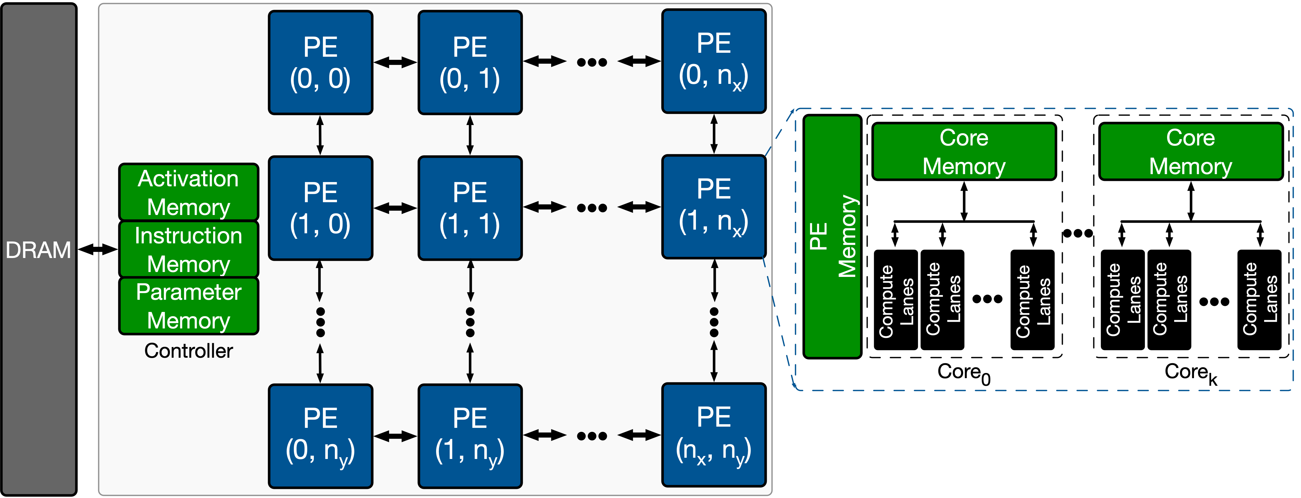
This memory, shown as PE memory in Figure 1, is mainly used to store model activations, partial results, and outputs. The cores within each PE feature a core memory that is mainly used for storing model parameters. Each core has multiple compute lanes where each lane has multi-way multiply-accumulate (MAC) units. The core memories are heavily multi-banked to keep up with the compute throughput of the parallel compute lanes and their SIMD MAC units. At each cycle, a set of activations are sent to the compute lanes. Then, the computations between the activations and model parameters are performed within each lane using the multi-way MAC units. Once the computations finish, the results are either stored back in the PE memory for further computation or are offloaded back into the DRAM.
3 Edge TPU Software Ecosystem
In this work we use TensorFlow Lite [24] based models as input to the Edge TPU software stack. Note that the software ecosystem varies based on the particular Edge TPU platform but [5] provides an overview of running TensorFlow Lite based inferences for the Coral Edge TPU platforms. The Edge TPU runtime library is used to communicate with the accelerator from the TensorFlow Lite (TFLite) API [5] where the TFLite models are compiled ahead-of-time using a publicly available Edge TPU compiler [3]. The main goal of the compiler is to map various neural network operations supported on the Edge TPU hardware while extracting the highest level of parallelism. Note that if the input models have unsupported or non-quantized operations, the compiler partitions the input graphs where the unsupported portion runs on a CPU instead of the Edge TPU.
Parameter caching. One critical optimization that the compiler performs is parameter caching [3]. As on-chip memory size is generally scarce on edge accelerators, efficiently managing this scratch-pad space is essential. For continuous inference scenarios, reloading the entire neural network model for every inference results in significant time spent on the memory transfers. If the parameters (i.e. weights) of the neural network are fully or partially cached in the on-chip memory, consecutive inferences on the new inputs can reuse the cached parameters. This process significantly reduces external memory transfers which leads to higher performance and energy efficiency.
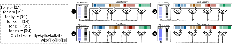
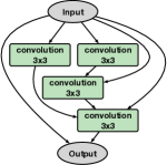
Mapping of convolution operation into accelerator. Figure 2 shows the loop nest of a convolutional layer (without batching) and its mapping onto an Edge TPU accelerator with one processing engine and four SIMD lanes. As depicted in Figure 2, the PE memory is used for both input activations, partial sums, and outputs. On the other hand, the core memory is exploited to store the weight parameters. Depending on the size of PE memory, core memory, input activations, weight parameters, and outputs, the compiler [3] may choose a different mapping and tiling for the data.
Figure 2 depicts an example showing the computation steps for performing a convolution operation on an Edge TPU accelerator. The squares with darker color show the data elements that are active at each particular computation step, whereas the squares with light color show the data elements that are inactive at a computation step. In this example, the input activation (in PE memory) has four elements. There are four weight parameters, each mapped onto a different core. The weight parameters also have four elements. Finally, the convolutional window size is (Kx = 1, Ky = 4, Zi = 1), and to compute one output element it requires all four elements of the input activation to be multiply-and-accumulated with all four elements of the weight parameters. Hence, in the loop nest representation, the and variables are set to one. At the first iteration ( ), the first element of the input activation and the first element of each of the (Zo = 4) kernels are multiplied together. The partial sum value is stored in the output array. Then ( ), the second element of the input activation and the second element of each kernel are multiplied together. The multiplication result is accumulated with the previous partial sum and stored back into the output array. The computation continues until all the elements of the input activation are processed ( ).
4 Learned Performance Model
In this paper, we use graph neural networks [34] to learn a generalized model for the performance of Edge TPUs across different convolutional neural networks. This work explores generalization across different neural network architectures and shows the feasibility of employing unique machine learning models for performance prediction across different accelerators. We use an in-house detailed cycle-accurate performance model to collect training data for the learned model (See Section 5 for details). Using graph neural networks, we learn a latent representation for each convolutional neural network. This latent representation is later used to estimate various performance metrics (e.g. latency and energy).
A convolutional neural network can be presented with a graph , where is a set of nodes that represent the valid operations (e.g. 33 convolution, 11 convolution, 33 max-pooling, input, and output), is a set of edges that represent the connectivity between the operations, and that is a vector serving as a graph global feature. A graph neural network takes as input the feature description of the nodes, an adjacency matrix, and a global feature of the graph and performs multiple iterations of message-passing [34] to learn a node-level representation. The learned node representations are aggregated into a graph-level representation using arithmetic operators such as summation or averaging [25, 10]. This graph-level representation is used as the performance model predictor. In the next paragraph, we elaborate the structure of our graph-based performance predictor.
4.1 Learned Performance Model Structure
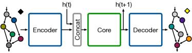
Recent work has explored employing various machine learning or analytical models for performance estimation [37, 17, 11, 38, 44, 42, 14, 50, 39, 7, 12, 23, 43, 22, 41, 26, 32, 6, 40, 46, 45, 29, 19, 49, 53, 27, 55, 36] of different applications and/or hardware accelerators. In this work, to implement the learned performance model, we use DeepMind’s Graph Nets [10] and Sonnet [18] libraries. We use a graph-based model because (a) application mapping is more straightforward and (b) graph neural networks generally better capture the dependencies between nodes [32, 48]. Figure 3 depicts the overall structure of the graph-based learned performance model. The model consists of three main components, namely encoder, core, and decoder, each serving as a neural network model. The encoder (decoder) network independently encodes (decodes) the edge, node, and global attributes. Note that, neither encoder nor decoder compute the structural relations between the graph components. The core component of the model performs multiple rounds of message-passing steps. After the core component computations complete, the structural relations between the graph components are learned and mapped into a node-level and/or graph-level representation.
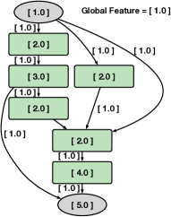
Input graph representation. Figure 4 shows a randomly selected cell from one of the convolutional neural network models in NASBench-101 [54] and its corresponding node, edge, and global feature vectors. We employ a simple float-encoding for the valid operations in the graph. We map input, 33 convolution, 33 max-pooling, 11 convolution, and output nodes to feature vector [1.0] to [5.0], respectively. In our current mapping, we do not differentiate between the edges and set all the edge features to [1.0]. Finally, for the graph-level representation, we use global feature vector [1.0].
Encoder/decoder components. The encoder/decoder components independently apply neural network models to edge, node, and global attributes. In our learned performance model, we use two-layered feed-forward neural networks each with 16 neurons, followed by a layer normalization [9] for edge, node, and global features.
Core component. The core component, as its name indicates, is the core computation part of the learned performance model. To better understand the architecture of the core component, we summarize the Graph Net library [10] block-structure concept that is used as building block for implementing flexible graph neural networks. Graph Net [10] consists of three main neural model blocks, namely edge, node, and global. The edge, node, and global neural model blocks use edge, node, and global attributes as their output. That is, after applying each neural model block, the corresponding output attribute gets updated. Using this methodology, various graph neural network architectures can be implemented simply by gluing these neural model blocks together. Generally, the computation steps in a full graph neural network block (See Algorithm 1 [10]) is as follows:
-
•
Edge update. Apply the edge neural model block on each edge and update its attribute based on the previous edge features, the features of the adjacent nodes, and the global feature of the graph;
-
•
Node update. Apply the node neural model block on each node and update its attribute based on the previous node features, the features of incoming edges, and the global feature of the graph;
-
•
Global update. Apply the global neural model block on the global feature and update its attribute based on the previous global feature, globally aggregated features of the edges, and globally aggregated features of the nodes.
The inputs to each neural model block and the aggregation type can be tailored to the demands of the target task. In our implementation, we use the default configurations for edge, node, and global blocks. In addition, we use the default summation operation as the aggregator for edge, node, and global neural model blocks. We use the final updated global attribute (a single float scalar) as the predicted performance metric (e.g. latency, energy, area, etc.).
5 Methodology
| Trainable Parameters Intervals | of Models |
|---|---|
| 227,274 — 5,202,474 | 210,673 |
| 5,202,474 — 10,177,674 | 102,488 |
| 10,177,674 — 15,152,874 | 44,272 |
| 15,152,874 — 20,128,074 | 3,513 |
| 20,128,074 — 25,103,274 | 38,003 |
| 25,103,274 — 30,078,474 | 4,413 |
| 30,078,474 — 35,053,674 | 15,041 |
| 35,053,674 — 40,028,874 | 3,533 |
| 40,028,874 — 45,004,074 | 1,209 |
| 45,004,074 — 49,979,274 | 479 |
Workloads. We use NASBench-101 [54] dataset that include nearly 423K unique convolutional neural network architectures with diverse structures and various number of convolutional operations. NASBench dataset are widely used in AutoML evaluation efforts [13, 52, 47, 28, 51, 15]. The valid operations in these neural network architectures are 33 convolution, 11 convolution, and 33 max-pooling. The neural networks in the NASBench dataset consist of three stacks followed by a downsampling layer. Each stack has a repeated structure of cells. The space of cell architecture includes all possible directed acyclic graph combinations of valid operations while complying with input/output dimensional constraints. To restrict the search space, the maximum number of vertices and edges within each cell are set to seven and nine, respectively. The NASBench dataset also includes evaluated performance (e.g. training and validation accuracy) of the neural network architectures on CIFAR-10 image dataset [35] at different epochs (4, 12, 36, and 108) totalling 5M trained models. This enables studying the trade-offs between the performance of Edge TPUs and training/validation accuracy of neural network models. Table 1 illustrates the distribution of models across different intervals of trainable parameters, which covers a diverse set of model sizes with different characteristics (e.g. compute- and memory-intensive).
Accelerator configurations. Table 2 depicts several key microarchitectural features of the studied classes of Edge TPU accelerators. The system clock frequency of V1, V2, and V3 accelerators are 800 MHz, 1066 MHz, and 1066 MHz, respectively. Comparing the V2 and V3 accelerators, V3 has larger PE memory (2 MB vs. 384 KB), more cores per PE (8 vs. 1), while using fewer Y-PEs (1 vs. 4).
| V1 | V2 | V3 | |
|---|---|---|---|
| Clock Frequency (MHz) | 800 | 1066 | 1066 |
| # of (X, Y)-PEs | (4, 4) | (4, 4) | (4, 1) |
| PE Memory | 2 MB | 384 KB | 2 MB |
| # of Cores per PE | 4 | 1 | 8 |
| Core Memory | 32 KB | 32 KB | 8 KB |
| # of Compute Lanes | 64 | 64 | 32 |
| Instruction Memory | 16384 | 16384 | 16384 |
| Parameter Memory | 16384 | 8192 | 8192 |
| Activation Memory | 1024 | 1024 | 1024 |
| I/O Bandwidth (GB/s) | 17 | 32 | 32 |
| Peak TOPS | 26.2 | 8.73 | 8.73 |
Microarchitectural simulations. To provide a uniform simulation infrastructure across all the the accelerator configurations, we use an in-house fully-parameterized cycle-accurate performance model. The simulator measures the latency and energy of running the workloads for different accelerator configurations. To provide highest performance, in all the simulations, we enable parameter caching [3].
Learned performance model training. We train our graph network model with the Adam optimizer [33] using default parameters and learning rate of 1e-3. We randomly split the dataset (423K data points) into 60 training, 20 validation, and 20 testing. We use DeepMind Sonnet [18] and Graph Nets [10] library to implement the neural models. For edge, node, and global neural model blocks, we use two-layer feed-forward models with 16 neurons at each layer, followed by a normalization layer. Because of its simple architecture, the latency of the learned model to generate a prediction is on the order of milliseconds. We use the default zero initializer for the bias. For the weights, we use truncated random normal values with a standard deviation proportional to the number of input features [30]. For the normalization layer, we create variables to hold the scale and offset of the normalization. For the training loss, we compute the mean square of the prediction error from every iteration of the message passing in order to enable the model to converge faster across every iteration of message passing. In this work, we train separate GNN models per class of Edge TPU. Since NASBench-101 is constructed by repeated same cell architecture, for each NASBench-101 model we use the cell architecture as the input to the learned model111The source code of our implementations can be found under open-source license at https://github.com/google-research/google-research/tree/master/l2da..
| V1 | V2 | V3 | |
|---|---|---|---|
| Min. Latency () | 0.079111 (81.94) | 0.074647 (82.81) | 0.074647 (82.81) |
| Max. Latency () | 5.676561 (93.78) | 5.653848 (94.33) | 5.666214 (93.55) |
| Avg. Latency () | 0.9631 (N/A) | 1.03485 (N/A) | 1.0655 (N/A) |
| Min. Energy () | 0.198351 (81.94) | 0.170954 (81.94) | N/A |
| Max. Energy () | 23.807941 (93.66) | 23.462845 (92.97) | N/A |
| Avg. Energy () | 4.252673 (N/A) | 3.9127185 (N/A) | N/A |
| V1 | V2 | V3 | |
|---|---|---|---|
| Latency () | 4.633768 | 4.185697 | 4.535305 |
| Energy () | 19.894033 | 19.745373 | N/A |
6 Evaluation
Inference latency and energy measurements. We perform inference latency measurements for three different configurations of the Edge TPU accelerator across all NASBench-101 [54] models (423K models) yielding a total number of latency measurements of approximately 1.5 Million (3423K). The inference latency numbers measure the total inference time including off-chip accesses. Similarly, we measure total energy for the V1 and V2 configurations across all the NASBench models (423K models) yielding a total number of energy measurements of approximately 900K (2423K). At the time of submission, the energy model for V3 was not available.
Table 3 shows the summary of the latency and energy results for three studied Edge TPU configurations and across the NASBench models with at least 70 mean validation accuracy after 108 training epochs. The number of data points after this filtering is 417,454; more than 98.5 of the total number of data points (423K). Compared to other accelerator configurations, V2 performs better in terms of delivering the highest accuracy (94.33) with lower latency (5.65 ms). The high performance of this Edge TPU configuration is mainly attributed to its larger core memory (32 KB) and higher I/O bandwidth (32 GB/s). The results also depict an interesting trend for the average energy consumption between V1 and V2. Compared to class V1, V2 has less PE memory and more I/O bandwidth (Table 2), which may indicate more off-chip memory accesses. We attribute this trend to V1’s lower clock frequency and its lower average number of cycles to execute the models (1,584,211.2 in V1 vs. 2,080,014.9 in V2).
Table 4 shows the latency and energy consumption of the best model in terms of mean validation accuracy. The mean validation accuracy (defined in [54]) is calculated across the three repeats of training after 108 training epochs [54]. The results corroborate our initial observation that V2 is more efficient compared to other configurations.
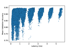
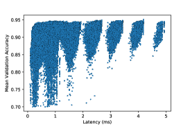
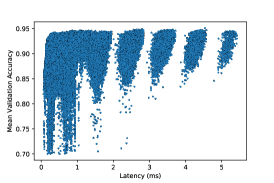
Figure 5 shows the comparison between mean validation accuracy and accelerator latency across all the convolutional models with at least 70 mean validation accuracy. As we can see, the data are clustered into different buckets. The number of 33 convolution operations in each NASBench cell is a key determinant of latency buckets. For example, an increase of one 33 convolution operation yields a jump from one latency bucket to the next one. The first three buckets (latency of 2.0 ms, 2.03.0 ms, and 3.04.0 ms, respectively) contain NASBench cells with respective averages of 1.48, 2.0, and 3.0 33 convolution operations.
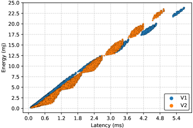
Figure 6 shows the relationship between the measured inference latency and inference energy for the NASBench models with at least 70 mean validation accuracy on the V1 and V2 configurations. The relationship between the latency and energy is linear. The first observation from Figure 6 is that for models with low latency ( 3.0 ms), V2 yields lower energy compared to V1. However, as latency increases (models with larger number of parameters), V1 consumes less energy. This trend can be attributed to the large PE memory size in V1 that enables running large models more efficiently. However, since V2 has smaller PE memory (only 384 KB), it may trigger multiple buffer flush/refills for these models.
. # of Models Average Latency (), Average Energy () V1 V2 V3 Latency(V1) 392725 0.80, 3.58 0.90, 3.58 0.92, N/A Latency(V2) 24325 3.73, 6.96 3.39, 15.67 3.61, N/A Latency(V3) 6570 2.59, 0.85 0.31, 0.64 0.25, N/A
Performance comparison of the accelerators. To compare the performance of the neural models across different configurations, we split the NASBench models into three buckets, one per accelerator configuration. Each bucket contains all the models whose measured latency is the least for that particular configuration, as shown in Table 5. For example, first row of the table shows all the models whose measured inference latency is the least on V1 compared to other accelerator configurations. First column of the table shows the number of models out of total NASBench models (423K) that reside in the corresponding bucket. Overall, V1 performs better (larger number of models) compared to other configurations in terms of latency. The next three columns show average latency and average energy of across the models that belong to the bucket for all three configurations. On average, for the models with higher latencies (second row), V2 performs better. Last bucket, in which V3 performs better compared to other accelerator configurations, mainly consists of models with a larger number of 11 convolution. On average, for the models in this bucket V3 yields 10.4 and 1.24 speedup compared to V1 and V2, respectively. The performance disparity between Edge TPU classes can be attributed to multiple application and/or accelerator characteristics. Table 6 highlights some of the differences between first and last bucket with respect to the model characteristics. The first bucket contains models with more parameters (higher memory-boundedness), due to more 33 convolution operations. V1 performs better because of its higher peak TOPs and larger on-chip memory. On the other hand, the last bucket contains models with fewer parameters. The differences between the frequency of V1 (800 MHz), V2 (1066 MHz), and V3 (1066 MHz) also contribute to the overall performance of each bucket.
| Latency(V1) | Latency(V3) | |
|---|---|---|
| Avg. of Conv 33 | 1.53 | 0.78 |
| Avg. of Conv 11 | 1.65 | 2.17 |
| Avg. of MaxPool 33 | 1.66 | 1.77 |
| Avg. Graph Depth | 4.96 | 4.64 |
| Avg. of Trainable Parameters | 7,054,471.34 | 1,417,485.36 |
| Accelerator | Latency |
|---|---|
| V1 | 4.633768 |
| V2 | 4.185697 |
| V3 | 4.535305 |

| Accelerator | Latency (Speedup) |
|---|---|
| V1 | 2.597874 (1.78) |
| V2 | 2.679829 (1.56) |
| V3 | 2.799071 (1.62) |
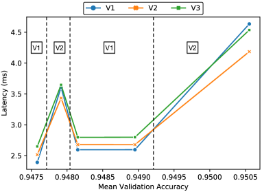
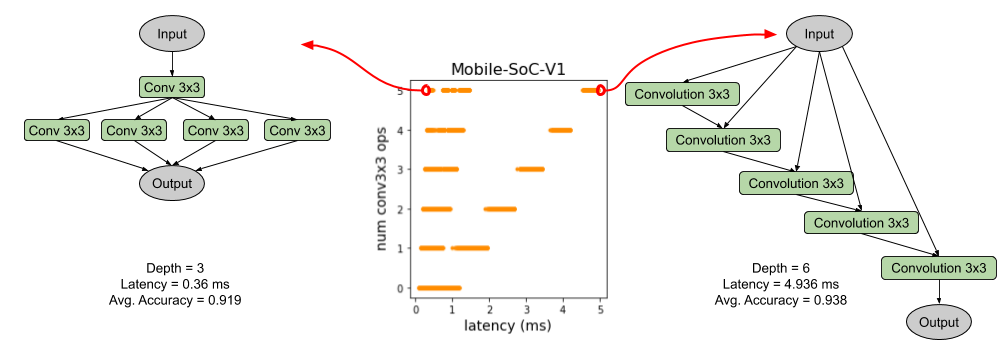
Analysis of models with high accuracy. Figure 7a illustrates the architecture of the NASBench cell that forms a convolutional neural model with the highest accuracy (95.055) in the NASBench dataset. Figure 7b annotates the neural architecture with the latency numbers across the three studied accelerators. V2 is the winner across all the accelerator configurations with the latency of 4.18 ms (10 less than V1 accelerator).
To better understand the trade-off between accuracy and latency, we also study the NASBench neural model with the second highest mean validation accuracy, shown in Figure 8a. The main observation here is that 0.16 trade-off in accuracy (95.055 94.895) yields up to 1.78 improvement in latency in V1. Note that, even though the accuracy degradation between these two neural models (Figure 7 and Figure 8) are minimal, there are 66% fewer parameters in the model shown in Figure 8, a key contributing factor to lower latency. Finally, it is interesting to observe that for the NASBench cell in Figure 8a V1 yields lower latency, in contrast to Figure 7a in which V2 performs better. We can attribute this result to (a) the lower I/O bandwidth in V1 that contributes more to reducing latency for neural models with fewer number of parameters and (b) the higher efficiency of V1 in running 11 convolution operations.
Analysis of accelerator performance for high-accuracy convolutional models. Figure 9 illustrates the comparison between latency and mean validation accuracy for the top five models with highest accuracy. The dashed lines in the figure split the curve into four regions showing which Edge TPU accelerator yields the lowest latency for that region. As mentioned before, for the highest accuracy model, V2 delivers the lowest latency. However, for the next two models, V1 is the winner. One of the main reasons for this trend is the type of operations that are used in each region. V1 generally performs better for the models with a larger number of 11 convolutional operators. Furthermore, this trend highlights the significant headroom for reducing the accelerator latency by slightly compromising the neural model accuracy.
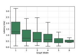
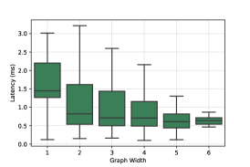
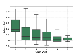
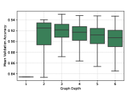
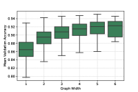
Neural model architecture impact on accelerator performance. First, we investigate the role of graph depth (Figure 10a) and graph width (Figure 10b) in terms of mean validation accuracy222Similar methodology used in NASBench-101 [54].. The whiskers in Figure 10 show that depth of three and width of five are optimal in terms of validation accuracy. The results also show that increasing depth beyond three has a negative impact on the accuracy of the model.
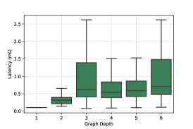
We also study the impact of graph structure on the accelerator latency across three Edge TPU configurations (Figure 11). The overall trend across all the accelerators shows that increasing graph depth increases latency, as the length of dependencies between operations increases. However, this trend breaks (latency decreases) for graph depth of four and five. On of the reason for such behavior is that the average number of model parameters for these graphs are lower (See Table 7) than other graph depths.
| Graph Depth | Avg. of Parameters |
|---|---|
| 3 | 7,442,469.77 |
| 4 | 6,144,266.36 |
| 5 | 6,399,201.72 |
| 6 | 8,428,092.52 |
However, increasing graph width generally results in lower latency, as it improves the parallelism between operations. Taking all of these results (graph structure, accuracy, and latency) into account, there is an interesting trade-off between model accuracy, accelerator performance, and graph structure. The results show that increasing the graph depth beyond a limit (three in our dataset) does not improve the model accuracy. However, increasing the graph width not only improves the model accuracy, but also tends to be more favorable in reducing the accelerator latency, mainly due to the higher parallelism between neural network operations.
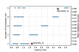
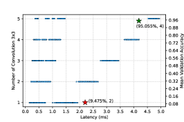
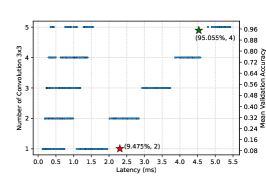
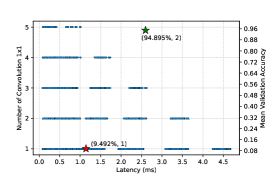
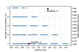
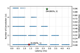
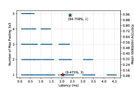
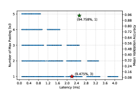
Correlation between latency and number of neural operations. To better understand the correlation between model complexity and accelerator performance, we further investigate the impact of operation types and number of trainable parameters on the accelerator latency. Figure 12 shows the impact of number of 33 convolution (first row), 11 convolution (second row), and 33 max pooling (third row) operations in each NASBench cell on inference latency across the studied accelerators. We also annotate each figure with the maximum (green star marker) and minimum (red star marker) achievable model accuracy for each category of operations. The highlighted values in parenthesis are (mean validation accuracy, the number of operations in the corresponding operation category). For example, Figure 12a shows that for the category of 33 convolution operations the maximum achievable model accuracy is 95.055 with four 33 convolution operation in the NASBench cell.
Due to the strict limit on the number of operations in each NASBench cell (seven), the latency increases as we increase the number of 33 convolution operations. This is because convolution 33 has higher number of parameters compared to other operations (e.g. convolution 11 and MaxPool 33). Hence, convolution 33 impacts latency more. In NASBench dataset, fewer convolution 11 / MaxPool 33 operations generally leads to more convolution 33 (more parameters). However, for the same number of 33 convolution operations in a NASBench cell, the latency numbers range from 0.2 ms to 5 ms. Figure 13 shows an example of two NASBench cell, one for each case. For the cases where the number of 33 convolution operations is high but the model depth is low, the inference latency will be low. If the number of 33 convolution operations and depth increase, the inference latency increases significantly.
Correlation between latency and trainable parameters.
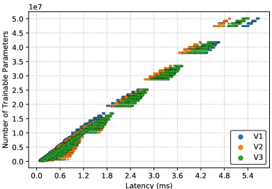
Figure 14 shows the relationship between the number of trainable parameters in the NASBench models and their respective inference latency on three different configurations of the Edge TPU accelerator. As increased number of trainable parameters comes with more MAC operations, for all three configurations the latency is mostly directly proportional to the number of trainable parameters. However, we observe that the ranking of the three configurations change at different model sizes. This is mainly explained by the interplay between parameter caching optimization (see Section 3) and the available memory bandwidth.
For very small models, all three configurations can cache the entire model which makes the overall latency very small. For this region, overall the inference latencies are very close to each other for all configurations. For the medium size models (5-30 million parameters), we observe that the V1 configuration provides the best performance. This is mainly attributed to its larger on-chip SRAM which can cache larger portions of the model whereas the other two configurations mostly end up streaming the parameters from off-chip.
Interestingly, there is a cross-over point for larger models where the parameter caching has diminishing returns and parameters streamed from off-chip dominates the latency. For these large models we observe that V2 and V3 provide better performance as they have larger memory bandwidth compared to V1. The difference between V2 and V3 configurations is mainly attributed to their architecture style. Although their peak TOPS and bandwidth are the same, V2 achieves that with using more PEs whereas V3 uses less PEs but more cores per PE. Having more PEs leads to fewer shared resources, less contention as well as more on-chip interconnect bandwidth, which enables V2 to sustain higher bandwidth.
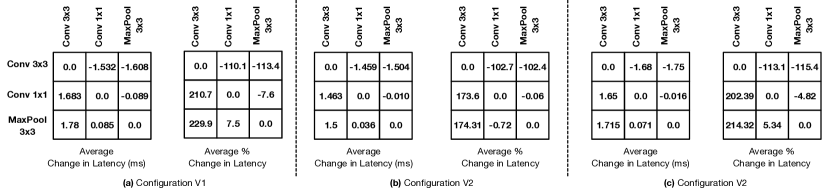
Performance and accuracy impact of operations. In Figure 15, we investigate the effect of swapping each pair of the cell operations (33 convolution, 11 convolution, and 33 max-pooling) on the performance of each class of accelerators. For this swap, for every NASBench cell, we replace each cell operation with another operation to obtain a new set of cell operations. Then, we search the NASBench dataset for a cell whose operations match the newly created cell operations and whose adjacency matrix matches the original cell’s adjacency matrix. The latency difference between these two cells are computed and averaged to obtain the latency impact of replacing cell operations. In a limited number of cases, the newly created cell operations does not match any existing cell in the the NASBench dataset, due to a mismatch between the number of input/output operations. In such cases, the performance and mean validation accuracy difference measurement is skipped.
Figure 15 shows the latency change when operations are replaced with the aforementioned methodology. Replacing a 11 convolution with a 33 increases the latency on all configurations but it increases the least (173.63%) for the V2 architecture. Changes in latency are not symmetric with respect to the swapping of cell operations. For example, the latency reduction caused by changing a 11 convolution to a 33 convolution is not equal to the latency increase caused by changing a 33 convolution to 11 convolution. This is because the changes in latency are measured by simulating and training the entire graph. The entire graph includes other operations and these other operations also contribute towards the graph’s overall performance.
. V1 V2 V3 Learning Rate 0.001 0.001 0.001 Batch Size 16 16 16 Training Set Size 254160 254160 254160 Test Set Size 84680 84680 84680 Avg. Accuracy 0.968 0.979 0.964 Spearman Correlation 0.99977 0.99981 0.99925 Pearson Correlation 0.99959 0.99974 0.99975
Accuracy of learned performance models. As mentioned in Section 4, we develop a learned model to estimate the various performance metrics of the accelerators. In this section, we investigate the learned model accuracy in estimating the latency of NASBench model across three studied Edge TPU configurations. Table 8 summarizes the training hyperparameters for the graph-based learned performance model. In addition, it shows the performance of the learned model in predicting the inference latency of the NASBench models across the studied accelerator configurations. The average accuracy of the learned model in estimating the inference latency is around 96%. We also report both the Spearman rank-order correlation and Pearson linear correlation metrics of the learned performance model with the ground truth latency numbers for each accelerator configurations. The results show that the learned model yields high correlation with the ground truth values ( 0.99). This strong correlation, especially the Spearman rank-order correlation, signifies that the learned performance model is a strong candidate for replacing the expensive-to-evaluate cycle-accurate simulators in design space exploration and hardware/software co-optimization approaches. This is because design space exploration and hardware/software co-optimization approaches only need to rank different configurations instead of measuring the absolute values.
6.1 Architectural Insights for Edge TPUs
High-performing accelerator for large models. For models with larger graph depth and/or with more 33 convolution operations (larger number of trainable parameters), accelerator configuration V2 yields lower latency as a result of its higher I/O bandwidth. For these large models, in general, parameter caching does not help. That is, when the number of trainable parameters are large, parameter caching leads to diminishing returns. However, when the models have a smaller number of trainable parameters, parameter caching helps. This results in better performance by accelerator configuration V1.
Impact of accelerator tile size on performance. For convolutional neural networks in the NASBench dataset, the latency is directly proportional to the number of trainable parameters. Even though the inference latency of these neural models are dependent on the neural architecture or graph structure, the number of trainable parameters has higher impact on inference latency. Therefore, it seems that I/O bandwidth is the deciding factor and other microarchitecture features (e.g. the number of PEs and compute cores) have lower impact on the overall accelerator latency. To summarize, for the neural models in the NASBench dataset, we can reduce the accelerator tile size and still achieve a similar performance.
7 Conclusion
This paper evaluates three different classes of Edge TPU accelerators, covering various computing ecosystems, across more than 423K unique convolutional neural networks. Analyzing these results, we draw critical and interpretable microarchitectural insights that help understand the architectural trade-offs in Edge TPUs. Finally, we discuss our proposed robust learned models to estimate the major performance metrics of Edge TPU accelerators. We show that the graph-based learned performance model estimates the latency and energy consumption of three studied classes of Edge TPUs with around 97% accuracy and high correlations (99) with the ground truth data. This high-accuracy learned model paves the way for rapid architecture exploration and hardware/software co-design, which we leave as future work.
Acknowledgment
We would like to extend our gratitude towards Suyog Gupta, Samy Bengio, Cliff Young, Chandu Thekkath, Stella Aslibekyan, the “Learn to Design Accelerators” team, and the extended Google Research Brain Team for their invaluable feedback and comments.
References
- [1] “Coral,” https://coral.ai/, accessed: 2022-09-30.
- [2] “Edge TPU,” https://cloud.google.com/edge-tpu, accessed: 2021-01-09.
- [3] “Edge TPU Compiler,” https://coral.ai/docs/edgetpu/compiler/#system-requirements, accessed: 2021-01-09.
- [4] “Introducing the Next Generation of On-Device Vision Models: MobileNetV3 and MobileNetEdgeTPU,” https://ai.googleblog.com/2019/11/introducing-next-generation-on-device.html, accessed: 2021-01-09.
- [5] “Run Inference on the Edge TPU with Python,” https://coral.ai/docs/edgetpu/tflite-python/#overview, accessed: 2021-01-09.
- [6] A. Adams, K. Ma, L. Anderson, R. Baghdadi, T.-M. Li, M. Gharbi, B. Steiner, S. Johnson, K. Fatahalian, F. Durand, and J. Ragan-Kelley, “Learning to Optimize Halide with Tree Search and Random Programs,” TOG, 2019.
- [7] V. S. Adve and M. K. Vernon, “Parallel Program Performance Prediction using Deterministic Task Graph Analysis,” TOCS, 2004.
- [8] Apple, “M1 Processor,” https://www.apple.com/mac/m1/, 2021.
- [9] J. L. Ba, J. R. Kiros, and G. E. Hinton, “Layer Normalization,” arXiv preprint arXiv:1607.06450, 2016.
- [10] P. W. Battaglia, J. B. Hamrick, V. Bapst, A. Sanchez-Gonzalez, V. Zambaldi, M. Malinowski, A. Tacchetti, D. Raposo, A. Santoro, R. Faulkner, C. Gulcehre, F. Song, A. Ballard, J. Gilmer, G. Dahl, A. Vaswani, K. Allen, C. Nash, V. Langston, C. Dyer, N. Heess, D. Wierstra, P. Kohli, M. Botvinick, O. Vinyals, Y. Li, and R. Pascanu, “Relational Inductive Biases, Deep Learning, and Graph Networks,” arXiv preprint arXiv:1806.01261, 2018.
- [11] A. D. Biagio and M. Davis, “LLVM Machine Code Analyzer,” https://llvm.org/docs/CommandGuide/llvm-mca.html, 2019, accessed: 2020-09-10.
- [12] V. Blanco, J. A. González, C. León, C. Rodrıguez, G. Rodrıguez, and M. Printista, “Predicting the Performance of Parallel Programs,” Parallel Computing, 2004.
- [13] J. Chang, X. Zhang, Y. Guo, G. Meng, S. XIiang, and C. Pan, “DATA: Differentiable ArchiTecture Approximation,” in NeurIPS, 2019.
- [14] X. E. Chen and T. M. Aamodt, “A First-order Fine-grained Multithreaded Throughput Model,” in HPCA, 2009.
- [15] H.-P. Cheng, T. Zhang, S. Li, F. Yan, M. Li, V. Chandra, H. Li, and Y. Chen, “NASGEM: Neural Architecture Search via Graph Embedding Method,” arXiv preprint arXiv:2007.04452, 2020.
- [16] E. Chung, J. Fowers, K. Ovtcharov, M. Papamichael, A. Caulfield, T. Massengill, M. Liu, D. Lo, S. Alkalay, M. Haselman, M. Abeydeera, L. Adams, H. Angepat, C. Boehn, D. Chiou, O. Firestein, A. Forin, K. S. Gatlin, M. Ghandi, S. Heil, K. Holohan, A. El Husseini, T. Juhasz, K. Kagi, R. K. Kovvuri, S. Lanka, F. van Megen, D. Mukhortov, P. Patel, B. Perez, A. Rapsang, S. Reinhardt, B. Rouhani, A. Sapek, R. Seera, S. Shekar, B. Sridharan, G. Weisz, L. Woods, P. Yi Xiao, D. Zhang, R. Zhao, and D. Burger, “Serving DNNs in Real Time at Datacenter Scale with Project Brainwave,” IEEE Micro, 2018.
- [17] I. Corporation, “Intel Architecture Code Analyzer,” https://software.intel.com/content/www/us/en/develop/articles/intel-architecture-code-analyzer.html, 2019, accessed: 2020-09-10.
- [18] DeepMind, “Sonnet,” https://github.com/deepmind/sonnet, 2021.
- [19] C. Dubach, J. Cavazos, B. Franke, G. Fursin, M. F. O’Boyle, and O. Temam, “Fast Compiler Optimisation Evaluation using Code-feature based Performance Prediction,” in CF, 2007.
- [20] EETimes, “AWS Rolls Out AI Inference Chip,” https://www.eetimes.com/aws-rolls-out-ai-inference-chip/, 2021.
- [21] Facebook, “Accelerating Facebook’s Infrastructure with Application-specific Hardware,” https://engineering.fb.com/2019/03/14/data-center-engineering/accelerating-infrastructure/, 2021.
- [22] T. Fahringer and H. P. Zima, “A Static Parameter based Performance Prediction Tool for Parallel Programs,” in ICS, 1993.
- [23] C. Ferdinand, R. Heckmann, M. Langenbach, F. Martin, M. Schmidt, H. Theiling, S. Thesing, and R. Wilhelm, “Reliable and Precise WCET Determination for a Real-life Processor,” in International Workshop on Embedded Software, 2001.
- [24] Google, “ML for Mobile and Edge Devices - TensorFlow Lite,” https://www.tensorflow.org/lite, 2021.
- [25] W. Hamilton, Z. Ying, and J. Leskovec, “Inductive Representation Learning on Large Graphs,” in NeurIPS, 2017.
- [26] F. Hartleb and V. Mertsiotakis, “Bounds for the Mean Runtime of Parallel Programs,” in Proceedings of the Sixth International Conference on Modelling Techniques and Tools for Computer Performance Evaluation, 1992.
- [27] K. Hegde, P.-A. Tsai, S. Huang, V. Chandra, A. Parashar, and C. W. Fletcher, “Mind Mappings: Enabling Efficient Algorithm-Accelerator Mapping Space Search,” in ASPLOS, 2021.
- [28] H. Hu, J. Langford, R. Caruana, S. Mukherjee, E. J. Horvitz, and D. Dey, “Efficient Forward Architecture Search,” in NeurIPS, 2019.
- [29] L. Huang, J. Jia, B. Yu, B.-G. Chun, P. Maniatis, and M. Naik, “Predicting Execution Time of Computer Programs using Sparse Polynomial Regression,” in NeurIPS, 2010.
- [30] S. Ioffe and C. Szegedy, “Batch Normalization: Accelerating Deep Network Training by Reducing Internal Covariate Shift,” arXiv preprint arXiv:1502.03167, 2015.
- [31] N. P. Jouppi, C. Young, N. Patil, D. Patterson, G. Agrawal, R. Bajwa, S. Bates, S. Bhatia, N. Boden, A. Borchers, R. Boyle, P.-l. Cantin, C. Chao, C. Clark, J. Coriell, M. Daley, M. Dau, J. Dean, B. Gelb, T. V. Ghaemmaghami, R. Gottipati, W. Gulland, R. Hagmann, C. R. Ho, D. Hogberg, J. Hu, R. Hundt, D. Hurt, J. Ibarz, A. Jaffey, A. Jaworski, A. Kaplan, H. Khaitan, D. Killebrew, A. Koch, N. Kumar, S. Lacy, J. Laudon, J. Law, D. Le, C. Leary, Z. Liu, K. Lucke, A. Lundin, G. MacKean, A. Maggiore, M. Mahony, K. Miller, R. Nagarajan, R. Narayanaswami, R. Ni, K. Nix, T. Norrie, M. Omernick, N. Penukonda, A. Phelps, J. Ross, M. Ross, A. Salek, E. Samadiani, C. Severn, G. Sizikov, M. Snelham, J. Souter, D. Steinberg, A. Swing, M. Tan, G. Thorson, B. Tian, H. Toma, E. Tuttle, V. Vasudevan, R. Walter, W. Wang, E. Wilcox, and D. H. Yoon, “In-data Center Performance Analysis of a Tensor Processing Unit,” in ISCA, 2017.
- [32] S. Kaufman, P. Phothilimthana, Y. Zhou, C. Mendis, S. Roy, A. Sabne, and M. Burrows, “A Learned Performance Model for Tensor Processing Units,” MLSys, 2021.
- [33] D. P. Kingma and J. Ba, “Adam: A Method for Stochastic Optimization,” arXiv preprint arXiv:1412.6980, 2014.
- [34] T. N. Kipf and M. Welling, “Semi-supervised Classification with Graph Convolutional Networks,” arXiv preprint arXiv:1609.02907, 2016.
- [35] A. Krizhevsky and G. Hinton, “Learning Multiple Layers of Features from Tiny Images,” 2009.
- [36] A. Kumar, A. Yazdanbakhsh, M. Hashemi, K. Swersky, and S. Levine, “Data-Driven Offline Optimization For Architecting Hardware Accelerators,” ICLR, 2022.
- [37] J. Laukemann, J. Hammer, G. Hager, and G. Wellein, “Automatic Throughput and Critical Path Analysis of x86 and ARM Assembly Kernels,” in PMBS, 2019.
- [38] J. Laukemann, J. Hammer, J. Hofmann, G. Hager, and G. Wellein, “Automated Instruction Stream Throughput Prediction for Intel and AMD Microarchitectures,” in PMBS, 2018.
- [39] X. Li, Y. Liang, T. Mitra, and A. Roychoudhury, “Chronos: A Timing Analyzer for Embedded Software,” Science of Computer Programming, 2007.
- [40] C. Mendis, A. Renda, S. P. Amarasinghe, and M. Carbin, “Ithemal: Accurate, Portable and Fast Basic Block Throughput Estimation using Deep Neural Networks,” in ICML, 2019.
- [41] C. Y. Park, “Predicting Program Execution Times by Analyzing Static and Dynamic Program Paths,” Real-Time Systems, 1993.
- [42] A. Patel, F. Afram, S. Chen, and K. Ghose, “MARSS: A Full System Simulator for Multicore x86 CPUs,” in DAC, 2011.
- [43] R. Rugina and K. E. Schauser, “Predicting the Running Times of Parallel Programs by Simulation,” in IPDPS, 1998.
- [44] D. Sanchez and C. Kozyrakis, “ZSim: Fast and Accurate Microarchitectural Simulation of Thousand-core Systems,” ACM SIGARCH Computer architecture news, 2013.
- [45] S. A. Seshia and J. Kotker, “GameTime: A Toolkit for Timing Analysis of Software,” in TACAS, 2011.
- [46] S. A. Seshia and A. Rakhlin, “Quantitative Analysis of Systems using Game-theoretic Learning,” TECS, 2012.
- [47] A. Shaw, W. Wei, W. Liu, L. Song, and B. Dai, “Meta Architecture Search,” in NeurIPS, 2019.
- [48] Z. Shi, K. Swersky, D. Tarlow, P. Ranganathan, and M. Hashemi, “Learning Execution Through Neural Code Fusion,” arXiv preprint arXiv:1906.07181, 2019.
- [49] O. Sýkora, P. M. Phothilimthana, C. Mendis, and A. Yazdanbakhsh, “GRANITE: A Graph Neural Network Model for Basic Block Throughput Estimation,” in IISWC, 2022.
- [50] T. M. Taha and S. Wills, “An Instruction Throughput Model of Superscalar Processors,” IEEE Transactions on Computers, 2008.
- [51] W. Wen, H. Liu, Y. Chen, H. Li, G. Bender, and P.-J. Kindermans, “Neural Predictor for Neural Architecture Search,” in ECCV, 2020.
- [52] C. White, W. Neiswanger, and Y. Savani, “BANANAS: Bayesian Optimization with Neural Architectures for Neural Architecture Search,” arXiv preprint arXiv:1910.11858, 2019.
- [53] A. Yazdanbakhsh, C. Angermueller, B. Akin, Y. Zhou, A. Jones, M. Hashemi, K. Swersky, S. Chatterjee, R. Narayanaswami, and J. Laudon, “Apollo: Transferable Architecture Exploration,” arXiv preprint arXiv:2102.01723, 2021.
- [54] C. Ying, A. Klein, E. Christiansen, E. Real, K. Murphy, and F. Hutter, “NAS-Bench-101: Towards Reproducible Neural Architecture Search,” in ICML, 2019.
- [55] Y. Zhou, X. Dong, T. Meng, M. Tan, B. Akin, D. Peng, A. Yazdanbakhsh, D. Huang, R. Narayanaswami, and J. Laudon, “Towards the Co-design of Neural Networks and Accelerators,” MLSys, 2022.