Material absorption-based carrier generation model for modeling optoelectronic devices
Abstract
The generation rate of photocarriers in optoelectronic materials is commonly calculated using the Poynting vector in the frequency domain. In time-domain approaches where the nonlinear coupling between electromagnetic (EM) waves and photocarriers can be accounted for, the Poynting vector model is no longer applicable. One main reason is that the photocurrent radiates low-frequency EM waves out of the spectrum of the source, e.g., terahertz (THz) waves are generated in THz photoconductive antennas. These frequency components do not contribute to the photocarrier generation since the corresponding photon energy is smaller than the optoelectronic material’s bandgap energy. However, the instantaneous Poynting vector does not distinguish the power flux of different frequency components. This work proposes a material absorption-based model capable of calculating the carrier generation rate accurately in the time domain. Using the Lorentz dispersion model with poles reside in the optical frequency region, the instantaneous optical absorption, which corresponds to the power dissipation in the polarization, is calculated and used to calculate the generation rate. The Lorentz model is formulated with an auxiliary differential equation method that updates the polarization current density, from which the absorbed optical power corresponding to each Lorentz pole is directly calculated in the time domain. Examples show that the proposed model is more accurate than the Poynting vector-based model and is stable even when the generated low-frequency component is strong.
Index Terms:
Auxiliary differential equation, generation rate, optoelectronic devices, optical absorption, photoconductive devices, photovoltaic devices, terahertz photoconductive antenna.I Introduction
Photoconductive devices (PCDs) and photovoltaic devices (PVDs) are important classes of optoelectronic devices [1, 2, 3]. These devices are widely used in industries. For instance, PVDs are used as solar cells and photosensors [3], and PCDs include terahertz (THz) photoconductive antennas (PCAs) and photodetectors. Simulation tools are indispensable in the development of these devices in the past decades. The recent development of nanostructured devices, such as plasmon-enhanced [4, 5, 6, 7], metasurface-integrated [7, 8], and nanostructure-textured devices [9, 10], calls for advanced numerical approaches that could accurately account for the nonlinear interactions between electromagnetic (EM) waves and carriers. The carrier densities in these devices are usually high such that the EM wave propagation and carrier dynamics are tightly coupled together [11, 12]. Modeling these devices requires solving a coupled system of Maxwell equations and carrier transport model, most frequently the drift-diffusion (DD) model [2, 3], and the solution should be carried out in the time domain due to the strong nonlinearity [11, 12, 13, 14].
One crucial mechanism in PCDs and PVDs is the generation of photocarriers upon absorption of the incident optical wave, which happens when the photon energy of the optical wave is high enough to excite electrons (typically larger than the bandgap energy of direct bandgap semiconductor materials) [1, 2, 3]. In device simulations, this mechanism is phenomenologically described by a generation rate model that depends on the optical power flux [1, 2, 3]. The generation rate can be estimated by the optical intensity, transmittance, and absorption coefficient in simple devices [1, 2, 3, 15, 16, 17, 18, 19, 20]. For complicated devices, the optical field distributions are inhomogeneous, and full-wave EM wave simulations are required. In this case, the generation rate can be calculated from the magnitude of the time-averaged Poynting vector, and it is done mostly in the frequency domain in the literature [21, 22, 23, 24, 25, 26, 27, 28, 29, 30, 31, 9, 32].
However, this approach is inadequate for more rigorous time-domain simulations that take into account the nonlinear couplings. The main reason is that the photocurrent resulting from freely moving photocarriers radiates low-frequency EM waves out of the optical source spectrum. Such low-frequency components can be strong in many devices, such as THz PCAs that are designed for converting optical energy to THz radiations [33, 34, 35, 36, 37], but their photon energy is not high enough to excite photocarriers, where is the Planck constant and is the frequency. Physically, the corresponding absorptance of the optoelectronic material is high at optical frequencies but negligible at low frequencies [38, 39, 40]. However, the time-dependent Poynting vector contains the power flux of the low-frequency components. Hence, the generation rate calculated from the Poynting vector is overestimated. Furthermore, the excessive photocarriers produce stronger low-frequency EM waves, leading to regenerative feedback.
In this work, we propose a new approach to calculate the space-time-dependent generation rate of photocarriers in optoelectronic materials. First, the optoelectronic material is modeled with the Lorentz dispersion model [41] that accounts for the optical absorption. The Lorentz model is formulated with an auxiliary differential equation (ADE) method in which the polarization current density is directly updated in the time integration. Then, the photocarrier generation rate is calculated using the instantaneous power dissipation expressed in terms of the polarization current density [42]. In the coupled Maxwell-DD system, the polarization current and photocurrent, which are responsible for the photon absorption and the low-frequency EM wave radiation, respectively, are updated separately in the ADE and the DD model. PCD simulation examples show that the proposed approach is more accurate than the Poynting vector-based model and is stable even when the generated low-frequency component is strong.
The rest of this paper is organized as follows. Section II introduces the proposed generation rate model, the modified ADE method for the Lorentz dispersion model, and the corresponding time integration scheme. Sections III presents numerical examples that validate the accuracy of the proposed model and demonstrate its applicability in PCDs. The reason for the failure of the Poynting vector-based model is also analyzed. Section IV provides a summary of this work.
II Formulation
II-A Generation Rate Model
The optical response and semiconductor carrier dynamics in PCDs and PVDs are commonly modeled with Maxwell equations and the DD model [21, 22, 23, 24, 25, 26, 27, 28, 29, 30, 31, 9, 32]. In the literature, Maxwell equations are solved for optical field distributions, which are then used for calculating the carrier generation rate in the DD model [21, 22, 23, 24, 25, 26, 27, 28, 29, 30, 31, 9, 32]. This two-step approach ignores moving carriers’ influence on optical fields and fails to capture saturation effects when the carrier density goes high [14]. To model the nonlinear couplings, we consider the fully-coupled time-dependent Maxwell-DD system [11, 12, 13, 14]
| (1) | ||||
| (2) | ||||
| (3) | ||||
| (4) |
where and are the vacuum permittivity and permeability, is the permittivity at the infinity frequency, is the relative permeability, and are the electric and magnetic fields, is the polarization current density, is the polarization density, is the DD current density, subscript represents the carrier type and the upper and lower signs should be selected for electron () and hole (), respectively, is the carrier density, is the current density due to carrier movements, and are the recombination and generation rates, and are the field-dependent mobility and diffusion coefficient [43], respectively, and are the steady-state electric field and carrier density resulting from the bias voltage and the doping profile [43, 12]. Here, and are assumed valid in the transient stage since the boundary conditions for Poisson and DD equations, e.g., the Dirichlet boundary conditions on the electrodes, do not change [44, 43] and the variation of EM fields due to photocarriers (including the DC response) is fully captured by solving Maxwell equations [14]. In (4), is the main driving force of the photocurrent, which produces THz radiations in PCAs [33, 12], while mainly causes local high frequency oscillations of photocarriers in the center of the device.
In (3), describes the generation rate of photocarriers upon absorption of optical EM wave energy [1, 2, 3]
| (5) |
where is the intrinsic quantum efficiency (number of electron-hole pairs generated by each absorbed photon), is the photon flux per unit volume, is the absorbed power density of optical waves, is the photon energy, is the Planck constant, and is the frequency of the optical wave. According to the photoelectric effect, must be high enough such that is large enough to excite electrons, e.g., usually should be larger than the bandgap energy in direct bandgap semiconductors [1, 2, 3].
In conventional devices, the optical pulse enters the semiconductor layer through a simple air-semiconductor interface, and can be estimated as [15, 16, 17, 18, 2, 19, 20, 3, 1]
| (6) |
where is the peak power flux of the optical pulse, is the transmittance at the air-semiconductor interface, is the absorption coefficient (sometimes the imaginary permittivity is used instead [22, 23]), is the penetration depth, and accounts for the spatial distribution and temporal delay of the optical pulse.
More frequently, complicated wave scatterings are involved in the optical wave propagation, one needs to solve the EM field distribution in the device and the Poynting vector (or equivalently in terms of ) is used to calculate [21, 22, 23, 24, 25, 26, 27, 28, 29, 30, 31, 9, 32]
| (7) |
where is the time-averaged Poynting vector, and are the phasors of electric and magnetic fields, and denote taking the real part and complex conjugate, respectively, accounts for the envelope of the source signal [2, 32, 22, 23]. In [32], is used instead of . Note that since is defined in the frequency domain, saying that at frequency , should be a slowly varying function as compared to . This means ’s of all frequencies in the narrowband associated with are approximated by that of (usually chosen as the center frequency of the source). In PVDs, usually a wide frequency band is considered, and is calculated at each sampling frequency, with , and weighted by the solar radiation spectrum [25, 26, 27, 28, 29, 30, 31, 9].
In practice, photocarriers strongly influence the EM fields, e.g., they induce a high conductivity that blocks the optical wave entering the device [14], and the photocurrent also radiates EM fields [33, 14]. calculated in the frequency domain cannot take into account such coupling effects [22, 14]. To calculate in the time domain, one may directly use the time-dependent Poynting vector
| (8) |
where , provided that a narrowband source is used [12]. However, the main issue in the time-domain calculation is that contains the power of all frequency components, including the low-frequency waves radiated from the photocurrent. For low-frequency waves, is smaller than , such that their power should not contribute to the generation rate of photocarriers.
To calculate corresponding to the optical frequency only, we consider the Poynting theorem for the system (1)–(4) [45]
| (9) |
where is the sum of electric and magnetic energy density (including that stored in the linear polarization and magnetization [45]), and are the power density associated with the conduction current density and the polarization current density, respectively [45]. It is easy to show that represents the conduction power loss [45], in which is calculated in the DD model (analogous to Ohm’s law). For a dispersive material, contains both the energy storage and dissipation in the polarization process. The power dissipation corresponds to the imaginary part of the permittivity, which is exactly the optical absorption in the case the positive imaginary permittivity is in the optical region.
To calculate the generation rate from the optical absorption, it is essential to separate the power dissipation from the energy storage in . In the following, we consider a multipole Lorentz model with poles reside in the frequency range of interest
| (10) |
where , , and are the resonant frequency, plasma frequency, and damping constant, respectively, is the number of poles. The corresponding electric flux density can be expressed as , where the polarization density , and satisfies
| (11) |
Expressing in terms of , and with , , is divided into two parts
| (12) |
where the first time derivative term is the time rate of change of the energy storage, which can be combined into in (9), and the second term, being positive and proportional to , is the power dissipation [45, 46, 42]. Moreover, the power dissipation associated with each pole can be calculated separately
| (13) |
and . Thus, the generation rate can be calculated as
| (14) |
II-B Time Integration
The ADE method for the Lorentz model has been well-studied in the literature, for example, see [41, 47] and references therein. Here, to directly calculate the power absorption, we define a slightly different ADE method that uses as the auxiliary variable. Equation (11) is rewritten as
| (15) | ||||
| (16) |
Equations (1)–(4) and (14)–(16) form the final system to be integrated over time. Due to the time-scale difference, the Maxwell system (1)–(2) and (15)–(16) and the DD system (3)–(4) are updated separately with independent schemes [12]. The low-storage five-stage fourth-order Runge-Kutta (RK) time integration scheme [48] is used for the Maxwell system
where is the time step size, and are RK coefficients, is solved from the DD solver. With the updated , and associated with each pole can be calculated readily at the end of the above RK loop. The DD system (3)–(4) is integrated in time using a third-order total-variation-diminishing RK scheme [49]. Since responses much slower than electromagnetic fields, the time step size for the DD system can be much larger [12]. The averaged generation rate is used in the DD solver, where is the ratio of the time step size between the DD and the Maxwell solver.
II-C Comments
It should be noted that, since in (5) and (14) explicitly depends on the frequency, it is not feasible to directly calculate the photon flux of a wideband optical pulse. In PCD simulations, this is not a problem since the source is rather narrowband (less than ) with its center frequency satisfying . One can use or to calculate the photon flux. For PVDs, usually, the frequency range of interest covers the full visible spectrum. Like in frequency-domain methods, one can run multiple simulations with different narrowband sources to cover the full frequency range. With the method proposed above, one can reduce the number of simulations using a wideband source together with a dispersion model consisting of multiple non-overlapping (in the frequency spectrum) poles, with each pole covering a narrow band. Note that one can also include other poles or dispersion models in other frequency ranges, however, only those poles contributing to the photoelectric effect (e.g., with ) should be included in (14).
III Numerical Results
III-A Optical Absorption
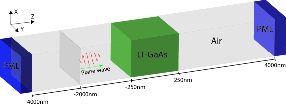
To validate the proposed generation rate model, we first verify the calculation of optical absorption through in an optoelectronic material. The model is shown in Fig. 1. An LT-GaAs layer of thickness nm is placed in air. Here, we focus on the optical properties of LT-GaAs, and the DD model is not considered. Periodic boundary conditions (PBCs) are used in the and directions and perfectly matched layers (PMLs) [50, 51, 52] are used in the direction. The relative permittivity of air is . The Lorentz model is used to fit the experimentally measured permittivity of LT-GaAs [38] in the frequency range . A single Lorentz pole, with parameters , , , , yields relative errors of and for the real and imaginary permittivity, respectively. All materials are considered nonmagnetic.
Consider a monochromatic plane wave with frequency THz, and linearly polarized in the direction, normally incident on the LT-GaAs layer. At THz, the complex relative permittivity is . The corresponding absorption coefficient is . Fig. 2 (a) shows calculated from (13), , and at . It shows is always positive, while and are oscillating between positive and negative values. Here, , and the negative value of means the instantaneous power flux is pointing to the negative direction. This is due to the reflection on the interface at the nm. When the scatterer is removed, stays positive. The oscillation of is due to the reactive power. Nevertheless, the time-averaged power flux of and should be the same since the power dissipation is totally included in . Indeed, after reached the steady state, the time-averaged power density calculated from , , and are , , and , respectively. This validates that correctly extracts all dissipated power from . It also indicates can approximate the power dissipation, however, it is less accurate than . Note that, in (8), the magnitude of is used for .
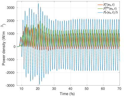
The same test is performed with a wideband pulsed source. A Gaussian pulse signal
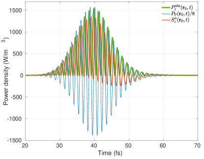
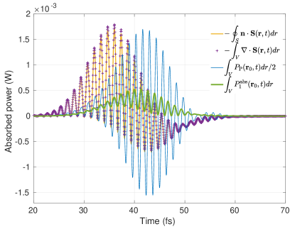
in which THz, fs, and , is used. Fig. 2 (b) shows , , and recorded at . Again, stays positive during the simulation while the other two models produce negative values. The accumulated power density (summed up over time) calculated from , , and are , , and , respectively. Furthermore, the total absorbed power in the LT-GaAs layer is shown in Fig. 2 (c), where and are the volume and surface of the LT-GaAs layer, respectively, and is the outward pointing unit normal vector on . From the Poynting theorem, both and give the instantaneous net value of the power entering the volume , and corresponds to the mechanic work in the polarization process. All of these three quantities are oscillating due to the reactive power. Their negative “tails” at the late time signifies the the physical process that the pulse energy gradually leaves the LT-GaAs layer. More importantly, is always positive, and, the total absorbed energy calculated from all those four expressions are the same ( J). This example shows Equation (13) works for wideband excitation as well.
III-B Carrier Generation in PCDs
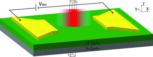
Next, the proposed method is used to model a PCD. The device is illustrated in Fig. 3. The photoconductive layer LT-GaAs and the substrate SI-GaAs have thickness nm, and their interface is located at . A bias voltage is applied on the electrodes. The distance between the electrodes along the direction is m. For LT-GaAs, the EM properties are the same as those in the previous example, and the semiconductor material properties are the same as those in [12]. The relative permittivity of SI-GaAs is . Here, we focus on the optoelectronic response and use a unit-cell model described in [13, 14]. First, the steady state of the semiconductor device under the bias voltage is solved from a coupled Poisson-DD system [43]. For Poisson equation, a potential-drop boundary condition is used along the direction to mimic the bias voltage, PBCs are used along the -direction, and a homogeneous Neumann boundary condition is used in the direction. For the stationary DD model, PBCs are used in both and directions, and a homogeneous Robin boundary condition is used on the surfaces of the LT-GaAs layer in the direction [53, 54]. The obtained steady-state electric field and field-dependent mobility are used as inputs in the transient Maxwell-DD solver [12, 14]. In the transient simulation, PBCs are used in and directions for Maxwell equations and the DD model. In the direction, PMLs are used for Maxwell equations, and a homogeneous Robin boundary condition is used for the DD model. More details about the unit-cell model can be found in [14].
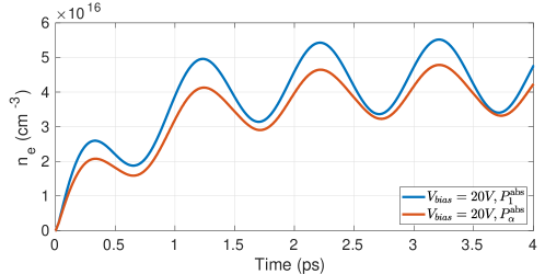
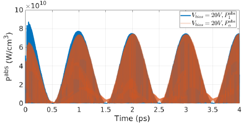
The PCD is excited by a continuous-wave source with two lasers operating at THz and THz and with axis linear polarization. The magnitude of photocarriers varies with the beat frequency THz, which leads to the radiation of THz EM waves. At low bias voltages and low power laser excitation, the models (6), (7), and (8) have been validated very well and found to agree with each other [20, 22, 55, 12]. Firstly, the proposed model is checked with a relatively low bias voltage V and a small laser power density . The time-dependent carrier densities calculated from the proposed model (13) and model (8) recorded at are shown in Fig. 4 (a). It shows the carrier densities calculated from these two models are on the same level. Fig. 4 (b) shows the corresponding instantaneous absorbed power density at in these two models. The observation is similar to the optical absorption shown in Fig. 2. Both models give similar results; however, the generation rate calculated from model (8) is less smooth (see the data near , , and ps) because of taking the magnitude of the Poynting vector.
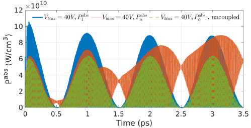
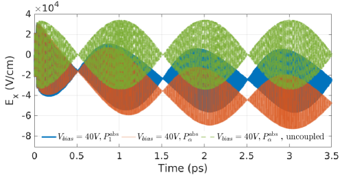
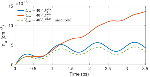
The photocurrent density depends on both the bias voltage and the power strength of the laser. Upon excitation with a higher power laser, which generates more photocarriers, and/or a higher bias voltage, which provides a larger drift force, the photocurrent becomes stronger and radiates stronger THz waves. Since the Poynting vector contains the THz wave power, the generation rate in model (8) is overestimated. To see this problem clearly, the same simulations as above are performed under a higher bias voltage V and with the same laser power. Fig. 5 (a) shows the power absorption calculated from both models. In model (8), the absorbed power keeps increasing and eventually becomes larger than the laser power. Apparently, this is unphysical since the source power is unchanged during the simulation. In the proposed model, the generation rate performs as expected. It stays at a stationary level after the laser power entered the device is stable.
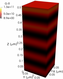
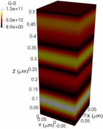
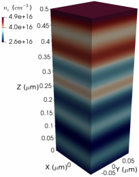
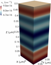
Fig. 5 (b) shows the electric field at under V. Clearly, the electric field contains a strong low-frequency component, which makes the mean value deviate from zero [14]. The low-frequency component is the radiation field resulting from the photocurrent [14]. The power absorption calculated from (8) follows the electric field, including the low-frequency parts. As discussed in Section I, physically, the low-frequency EM fields do not contribute to the carrier generation. The overestimated generation rate produces more low-frequency waves, which again leads to a higher generation rate in model (8). Fig. 5 (c) shows the carrier density produced by model (8) keeps increasing and eventually diverges.
For comparison, an “uncoupled” simulation, where the DD current density in (1) is removed, is done under the same settings as above using the model (8). The corresponding results are also shown in Fig. 5. In this case, no low-frequency EM waves are radiated and the power absorption calculated from (8) stays stable. This verifies that the previous unsaturated behavior in model (8) is a result of that the Poynting vector includes the power of low-frequency components.
In contrast, in Fig. 5, the power absorption calculated from the proposed method acts as expected. The material dispersion model only takes into account the optical absorption, which corresponds to the experimental permittivity that the absorptance of LT-GaAs at low-frequency is negligible. Meanwhile, the THz radiation resulting from the coupling can be modeled correctly. This provides us the ability to analyze the radiation field screening effect in PCDs [14, 33, 34, 35, 36, 37]. Even for the uncoupled simulation, as has been shown in the previous example, the proposed model is more accurate than the Poynting vector-based model.
Fig. 6 (a) and (b) show the spatial distributions of at ps under V calculated from the proposed model and model (8), respectively, and Fig. 6 (c) and (d) show corresponding electron densities. In the proposed model, the solutions decay smoothly as propagating in the negative direction. This is expected since the optical wave is absorbed by the material and screened by the photocarriers. The solutions calculated from model (8) are less smooth and, at this instant of time, the carrier density is higher near the bottom. From our tests, finer meshes are required for stability in the Poynting vector-based model, especially when the carrier density is high.
IV Conclusion
The strong nonlinear coupling between electromagnetic (EM) waves and photocarriers in optoelectronic devices calls for a time-domain numerical approach. A crucial step in the time-domain simulation is calculating the carrier generation rate from the optical EM fields. Because of the low-frequency EM field radiation from the photocurrents, the Poynting vector-based generation model overestimates the carrier generation and leads to an unsaturated carrier density.
This work proposes a material absorption-based generation rate model. First, the optoelectronic material is modeled with the Lorentz dispersion model with poles reside in the optical frequency region. Then, the carrier generation rate is calculated using the instantaneous optical absorption expressed in terms of the polarization current density. The ADE method for the Lorentz dispersion model is formulated such that the generation rate contributed by each Lorentz pole is updated efficiently in the time integration. PCD examples show that the proposed model is more accurate than the Poynting vector-based model and is stable even when the generated low-frequency component is strong. This model can be used for time-domain simulations of a wide range of optoelectronic devices, e.g., solar cells, photosensors, and photodetectors. Moreover, as the generation rate corresponding to each Lorentz pole can be calculated independently, a wideband simulation can be performed in the time domain using a multipole Lorentz model.
Acknowledgment
This work is supported by the King Abdullah University of Science and Technology (KAUST) Office of Sponsored Research (OSR) under Award No 2019-CRG8-4056. The authors would like to thank the KAUST Supercomputing Laboratory (KSL) for providing the required computational resources.
References
- [1] B. E. Saleh and M. C. Teich, Fundamentals of photonics. Hoboken, NJ, USA: John Wiley & Sons, 2019.
- [2] S. L. Chuang, Physics of photonic devices. John Wiley & Sons, 2012, vol. 80.
- [3] J. Piprek, Ed., Handbook of Optoelectronic Device Modeling and Simulation. Boca Raton: CRC Press, 2018.
- [4] S. Lepeshov, A. Gorodetsky, A. Krasnok, E. Rafailov, and P. Belov, “Enhancement of terahertz photoconductive antenna operation by optical nanoantennas,” Laser Photonics Rev., vol. 11, no. 1, p. 1600199, 2017.
- [5] J.-H. Kang, D.-S. Kim, and M. Seo, “Terahertz wave interaction with metallic nanostructures,” Nanophotonics, vol. 7, no. 5, pp. 763–793, 2018.
- [6] H. Yu, Y. Peng, Y. Yang, and Z.-Y. Li, “Plasmon-enhanced light–matter interactions and applications,” Npj Comput. Mater., vol. 5, no. 1, pp. 1–14, 2019.
- [7] A. E. Yachmenev, D. V. Lavrukhin, I. A. Glinskiy, N. V. Zenchenko, Y. G. Goncharov, I. E. Spektor, R. A. Khabibullin, T. Otsuji, and D. S. Ponomarev, “Metallic and dielectric metasurfaces in photoconductive terahertz devices: a review,” Opt. Eng., vol. 59, no. 6, p. 061608, 2019.
- [8] T. Siday, P. P. Vabishchevich, L. Hale, C. T. Harris, T. S. Luk, J. L. Reno, I. Brener, and O. Mitrofanov, “Terahertz detection with perfectly-absorbing photoconductive metasurface,” Nano Lett., vol. 19, no. 5, pp. 2888–2896, 2019.
- [9] Y.-P. Zhou, M.-J. Li, Y.-L. He, and Y.-S. Li, “Multi-physics analysis: The coupling effects of nanostructures on the low concentrated black silicon photovoltaic system performances,” Energy Convers. Manag., vol. 159, pp. 129 – 139, 2018.
- [10] Y.-L. He, Y.-P. Zhou, Y. huang Hu, and T.-C. Hung, “A multiscale-multiphysics integrated model to investigate the coupling effects of non-uniform illumination on concentrated photovoltaic system with nanostructured front surface,” Appl. Energy, vol. 257, p. 113971, 2020.
- [11] L. Chen and H. Bagci, “A discontinuous Galerkin framework for multiphysics simulation of photoconductive devices,” in Proc. Int. Appl. Comput. Electromagn. Symp. IEEE, 2019, pp. 1–2.
- [12] ——, “Multiphysics simulation of plasmonic photoconductive devices using discontinuous Galerkin methods,” IEEE J. Multiscale Multiphys. Comput. Tech., vol. 5, pp. 188–200, 2020.
- [13] L. Chen and H. Bagci, “A unit-cell discontinuous Galerkin scheme for analyzing plasmonic photomixers,” in Proc. IEEE Int. Symp. Antennas Propag., 2019, pp. 1069–1070.
- [14] L. Chen, K. Sirenko, and H. Bagci, “An efficient discontinuous Galerkin scheme for simulating terahertz photoconductive devices with periodic nanostructures,” arXiv preprint arXiv:2006.02141, 2020.
- [15] E. Sano and T. Shibata, “Fullwave analysis of picosecond photoconductive switches,” IEEE J. Quantum Electron., vol. 26, no. 2, pp. 372–377, 1990.
- [16] D. Saeedkia, A. H. Majedi, S. Safavi-Naeini, and R. R. Mansour, “Analysis and design of a photoconductive integrated photomixer/antenna for terahertz applications,” IEEE J. Quantum Electron., vol. 41, no. 2, pp. 234–241, 2005.
- [17] P. Kirawanich, S. J. Yakura, and N. E. Islam, “Study of high-power wideband terahertz-pulse generation using integrated high-speed photoconductive semiconductor switches,” IEEE Trans. Plasma Sci., vol. 37, no. 1, pp. 219–228, 2008.
- [18] P. Kirawanich, S. J. Yakura, and N. E. Islam, “Study of high-power wideband terahertz-pulse generation using integrated high-speed photoconductive semiconductor switches,” IEEE Trans. Plasma Sci., vol. 37, no. 1, pp. 219–228, 2009.
- [19] N. Khiabani, Y. Huang, Y.-C. Shen, and S. Boyes, “Theoretical modeling of a photoconductive antenna in a terahertz pulsed system,” IEEE Trans. Antennas Propag., vol. 61, no. 4, pp. 1538–1546, 2013.
- [20] E. Moreno, M. F. Pantoja, S. G. Garcia, A. R. Bretones, and R. G. Martin, “Time-domain numerical modeling of THz photoconductive antennas,” IEEE Trans. THz Sci. Technol., vol. 4, no. 4, pp. 490–500, 2014.
- [21] M. Neshat, D. Saeedkia, L. Rezaee, and S. Safavi-Naeini, “A global approach for modeling and analysis of edge-coupled traveling-wave terahertz photoconductive sources,” IEEE Trans. Microw. Theory Tech., vol. 58, no. 7, pp. 1952–1966, 2010.
- [22] N. Burford and M. El-Shenawee, “Computational modeling of plasmonic thin-film terahertz photoconductive antennas,” J. Opt. Soc. Am. B, vol. 33, no. 4, pp. 748–759, 2016.
- [23] M. Bashirpour, S. Ghorbani, M. Kolahdouz, M. Neshat, M. Masnadi-Shirazi, and H. Aghababa, “Significant performance improvement of a terahertz photoconductive antenna using a hybrid structure,” RSC Advances, vol. 7, no. 83, pp. 53 010–53 017, 2017.
- [24] A. Garufo, G. Carluccio, N. Llombart, and A. Neto, “Norton equivalent circuit for pulsed photoconductive antennas–part i: Theoretical model,” IEEE Trans. Antennas Propag., vol. 66, no. 4, pp. 1635–1645, 2018.
- [25] A. Deinega and S. John, “Finite difference discretization of semiconductor drift-diffusion equations for nanowire solar cells,” Comput. Phys. Commun., vol. 183, no. 10, pp. 2128 – 2135, 2012.
- [26] W. E. Sha, W. C. Choy, Y. Wu, and W. C. Chew, “Optical and electrical study of organic solar cells with a 2D grating anode,” Opt. Express, vol. 20, no. 3, pp. 2572–2580, Jan 2012.
- [27] X. Li, N. P. Hylton, V. Giannini, K.-H. Lee, N. J. Ekins-Daukes, and S. A. Maier, “Multi-dimensional modeling of solar cells with electromagnetic and carrier transport calculations,” Prog. Photovolt., vol. 21, no. 1, pp. 109–120, 2013.
- [28] M. G. Deceglie, V. E. Ferry, A. P. Alivisatos, and H. A. Atwater, “Design of nanostructured solar cells using coupled optical and electrical modeling,” Nano Lett., vol. 12, no. 6, pp. 2894–2900, 2012.
- [29] A. H. Fallahpour, G. Ulisse, M. Auf der Maur, A. Di Carlo, and F. Brunetti, “3-D simulation and optimization of organic solar cell with periodic back contact grating electrode,” IEEE J. Photovolt., vol. 5, no. 2, pp. 591–596, 2015.
- [30] S. In, D. R. Mason, H. Lee, M. Jung, C. Lee, and N. Park, “Enhanced light trapping and power conversion efficiency in ultrathin plasmonic organic solar cells: A coupled optical-electrical multiphysics study on the effect of nanoparticle geometry,” ACS Photonics, vol. 2, no. 1, pp. 78–85, 2015.
- [31] S. Ahn, D. Rourke, and W. Park, “Plasmonic nanostructures for organic photovoltaic devices,” J. Opt., vol. 18, no. 3, p. 033001, feb 2016.
- [32] M. Khabiri, M. Neshat, and S. Safavi-Naeini, “Hybrid computational simulation and study of continuous wave terahertz photomixers,” IEEE Trans. THz Sci. Technol., vol. 2, no. 6, pp. 605–616, 2012.
- [33] J. T. Darrow, X. C. Zhang, D. H. Auston, and J. D. Morse, “Saturation properties of large-aperture photoconducting antennas,” IEEE J. Quantum Electron., vol. 28, no. 6, pp. 1607–1616, 1992.
- [34] P. K. Benicewicz and A. J. Taylor, “Scaling of terahertz radiation from large-aperture biased inp photoconductors,” Opt. Lett., vol. 18, no. 16, pp. 1332–1334, Aug 1993.
- [35] D. S. Kim and D. S. Citrin, “Coulomb and radiation screening in photoconductive terahertz sources,” Appl. Phys. Lett., vol. 88, no. 16, p. 161117, 2006.
- [36] G. C. Loata, M. D. Thomson, T. Loffler, and H. G. Roskos, “Radiation field screening in photoconductive antennae studied via pulsed terahertz emission spectroscopy,” Appl. Phys. Lett., vol. 91, no. 23, p. 232506, 2007.
- [37] R.-H. Chou, C.-S. Yang, and C.-L. Pan, “Effects of pump pulse propagation and spatial distribution of bias fields on terahertz generation from photoconductive antennas,” J. Appl. Phys., vol. 114, no. 4, p. 043108, 2013.
- [38] J. S. Blakemore, “Semiconducting and other major properties of gallium arsenide,” J. Appl. Phys., vol. 53, no. 10, pp. R123–R181, 1982.
- [39] M. E. Levinshtein and S. L. Rumyantsev, “Silicon (si),” in Handbook Series On Semiconductor Parameters: Volume 1: Si, Ge, C (Diamond), GaAs, GaP, GaSb, InAs, InP, InSb. World Scientific, 1996, pp. 1–32.
- [40] H. S. Sehmi, W. Langbein, and E. A. Muljarov, “Optimizing the drude-lorentz model for material permittivity: Examples for semiconductors,” in Prog. in Electromagn. Res. Symp., 2017, pp. 994–1000.
- [41] A. Taflove and S. C. Hagness, Computational electrodynamics: the finite-difference time-domain method. MA, Norwood: Artech house, 2005.
- [42] T. J. Cui and J. A. Kong, “Time-domain electromagnetic energy in a frequency-dispersive left-handed medium,” Phys. Rev. B, vol. 70, p. 205106, Nov 2004.
- [43] L. Chen and H. Bagci, “Steady-state simulation of semiconductor devices using discontinuous Galerkin methods,” IEEE Access, vol. 8, pp. 16 203–16 215, 2020.
- [44] D. Vasileska, S. M. Goodnick, and G. Klimeck, Computational Electronics: semiclassical and quantum device modeling and simulation. Boca Raton, FL, USA: CRC press, 2010.
- [45] H. A. Haus and J. R. Melcher, Electromagnetic fields and energy. Prentice Hall Englewood Cliffs, NJ, 1989, vol. 107.
- [46] P. D. Smith and K. E. Oughstun, “Electromagnetic energy dissipation and propagation of an ultrawideband plane wave pulse in a causally dispersive dielectric,” Radio Sci., vol. 33, no. 6, pp. 1489–1504, 1998.
- [47] S. D. Gedney, J. C. Young, T. C. Kramer, and J. A. Roden, “A discontinuous Galerkin finite element time-domain method modeling of dispersive media,” IEEE Trans. Antennas Propag., vol. 60, no. 4, pp. 1969–1977, 2012.
- [48] J. Hesthaven and T. Warburton, Nodal Discontinuous Galerkin Methods: Algorithms, Analysis, and Applications. NY, USA: Springer, 2008.
- [49] C.-W. Shu and S. Osher, “Efficient implementation of essentially non-oscillatory shock-capturing schemes,” J. Comput. Phys., vol. 77, no. 2, pp. 439–471, 1988.
- [50] L. Chen, M. B. Ozakin, and H. Bagci, “A low-storage pml implementation within a high-order discontinuous Galerkin time-domain method,” in Proc. IEEE Int. Symp. Antennas Propag., 2020, pp. 1069–1070.
- [51] L. Chen, M. B. Ozakin, S. Ahmed, and H. Bagci, “A memory-efficient implementation of perfectly matched layer with smoothly-varying coefficients in discontinuous Galerkin time-domain method,” IEEE Trans. Antennas Propag., pp. 1–1, 2020.
- [52] S. D. Gedney, C. Luo, J. A. Roden, R. D. Crawford, B. Guernsey, J. A. Miller, T. Kramer, and E. W. Lucas, “The discontinuous Galerkin finite-element time-domain method solution of Maxwell’s equations,” Appl. Comput. Electromagn. Soc. J., vol. 24, no. 2, p. 129, 2009.
- [53] L. Chen, M. Dong, and H. Bagci, “Modeling floating potential conductors using discontinuous Galerkin method,” IEEE Access, vol. 8, pp. 7531–7538, 2020.
- [54] L. Chen, M. Dong, P. Li, and H. Bagci, “A hybridizable discontinuous Galerkin method for simulation of electrostatic problems with floating potential conductors,” Int. J. Numer. Model.: Electron. Networks, Device Fields, p. e2894, 2020.
- [55] M. Khorshidi and G. Dadashzadeh, “Plasmonic photoconductive antennas with rectangular and stepped rods: a theoretical analysis,” J. Opt. Soc. Am. B, vol. 33, no. 12, pp. 2502–2511, Dec 2016.