Swiss Nanoscience Institute, University of Basel, CH-4056, Basel, Switzerland
\alsoaffiliationSwiss Nanoscience Institute, University of Basel, CH-4056, Basel, Switzerland
\alsoaffiliationSwiss Nanoscience Institute, University of Basel, CH-4056, Basel, Switzerland
Superconducting contacts to a monolayer semiconductor
Abstract
We demonstrate superconducting vertical interconnect access (VIA) contacts to a monolayer of molybdenum disulfide (MoS2), a layered semiconductor with highly relevant electronic and optical properties. As a contact material we use MoRe, a superconductor with a high critical magnetic field and high critical temperature. The electron transport is mostly dominated by a single superconductor/normal conductor junction with a clear superconductor gap. In addition, we find MoS2 regions that are strongly coupled to the superconductor, resulting in resonant Andreev tunneling and junction dependent gap characteristics, suggesting a superconducting proximity effect. Magnetoresistance measurements show that the bandstructure and the high intrinsic carrier mobility remain intact in the bulk of the MoS2. This type of VIA contact is applicable to a large variety of layered materials and superconducting contacts, opening up a path to monolayer semiconductors as a platform for superconducting hybrid devices.
keywords: TMDC, van der Waals heterostructure, MoS2, monolayer semiconductor, superconducting contacts, superconducting proximity effect
Semiconductors combined with superconducting metals have become a most fruitful field for applications and fundamental research, from gate tunable superconducting qubits 1, thermoelectrics 2, 3, to prospective Majorana bound states, 4, 5 or sources of entangled electron pairs 6, 7, 8. These experiments were mainly developed based on one-dimensional (1D) nanowires. To obtain more flexible platforms and scalable architectures, recent efforts focused on two-dimensional (2D) semiconductors 9, 10, 11, 12, 13. However, the number of materials suitable for superconducting hybrids is rather limited. Potentially ideal and ultimately thin semiconductors with a large variety of properties can be found among transition metal dichalcogenides (TMDCs) grown in stacked atomically thin layers. TMDCs often exhibit a broad variety of interesting optical and electronic properties 14, 15, 16, for example the valley degree of freedom, potentially useful as qubits 17, 18, strong electron-electron 19, 20 and spin-orbit interactions 20, or crystals with topologically non-trivial bandstructures 21, 22. One promising material is the semiconductor , with a relatively high mobility and large mean free path, allowing for gate-defined nanostructures 23, 24, 25, which would make MoS2 an ideal platform to combine with superconducting elements.
MoS2 was used as tunnel barrier between superconductors in vertical heterostructures 26, 27 and showed signs of intrinsic superconductivity 28 and of a ferromagnetic phase at low electron densities 29. However, to exploit the intrinsic properties of MoS2 and to fabricate in-situ gate tunable superconducting hybrid structures, direct superconducting contacts in lateral devices are required. Such contacts are difficult to fabricate due to the formation of Schottky barriers 30, 31, 21, material degradation 32 and fabrication residues when using standard fabrication methods 33, 34, 24. Less conventional edge contacts were also found problematic recently 35.
Here, we report vertical access interconnect (VIA) contacts 36 to monolayer MoS2 with the superconductor MoRe as contact material. We demonstrate a clear superconducting gap in the transport characteristics, including the magnetic field and temperature dependence, and features suggesting stronger superconductor-semiconductor couplings, forming the basis for superconducting proximity effects and bound states. In addition, we show that this fabrication method retains the intrinsic MoS2 bulk properties, including a large electron mobility and sequentially occupied spin-orbit split bands 23.
Figure 1(a) shows an optical microscopy image of the presented device, and a schematic of a single VIA contact. The MoS2 is fully encapsulated by exfoliated hexagonal boron nitride (hBN), ensuring minimal contamination of the bulk materials, while the following assembly process allows the fabrication of pristine material interfaces and contacts:
1) vertical access: using electron beam lithography (EBL), VIA areas with a radius of nm are defined on the designated top hBN flake (nm thickness) on a Si/SiO2 wafer, and etched completely open by reactive ion etching with a 20:5:5 sccm SF6:O2:Ar mixture at mTorr chamber pressure and W RF power.
2) VIA metalization: in a second EBL step, a slightly larger area with the VIA in the center is defined for mechanical anchoring to the top hBN. We then deposit the type II superconductor MoRe (bulk critical temperature K, (second) critical magnetic field T 37, 38) using sputter techniques. As the optimal film thickness we find nm plus the top hBN thickness.
3) Stacking of layers: the wafer with the VIA structure is transferred to an inert gas (nitrogen) glove box, where the top hBN layer with the metalized VIAs is picked up from the substrate using a polycarbonate (PC) stamp and an hBN helper layer, and then used to pick up consecutively a monolayer MoS2 flake, a bottom hBN flake (nm thickness), and a multilayer graphene (MLG) flake serving as backgate.
4) Finish: the stack is then deposited onto a Si/SiO2 wafer, where macroscopic Ti/Au (nm) leads to the VIAs are fabricated using EBL. The sample is then annealed at 350∘C for 30 min, in a vacuum chamber with a constant flow of forming gas.
Using gold as VIA material, this fabrication process yields of the contacts with two-terminal resistance-area products smaller than k at K at a backgate voltage of V. This yield is reduced to roughly when using MoRe, possibly due to a material loss during the pick-up procedure. In the presented device, only half of the contacts show resistances lower than , which we use for the experiments and are labeled from C1 to C4 in Fig. 1(a). The two terminal differential conductances we obtain by measuring the current variation in the grounded contact Cj while applying a modulated bias voltage to contact Ck using standard lock-in techniques. The experiments were performed in a dilution refrigerator at mK, while for higher temperatures, we used a variable temperature insert (VTI) with a base temperature of K. In addition, we apply an external magnetic field perpendicular to the substrate.
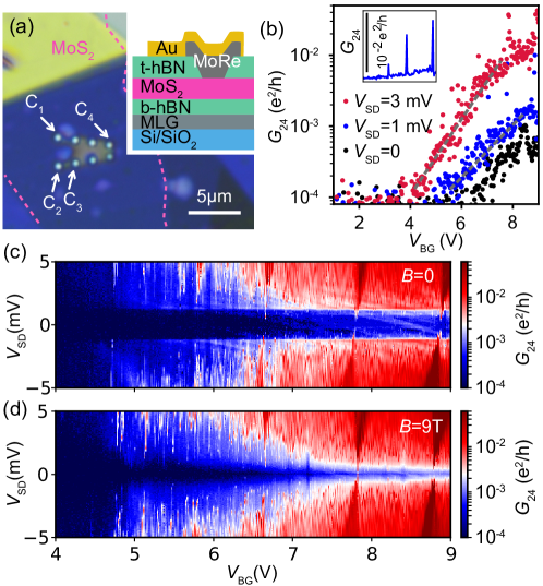
In Fig. 1(b), the differential conductance is plotted as a function of the backgate voltage for several bias voltages . Increasing results in an exponential increase in , starting from a pinch-off voltage of V for . This value is offset towards smaller values for larger bias voltages, a first indication for an energy gap. However, as seen in the inset of Fig. 1(b), in this regime we find very sharp peaks in , consistent with Coulomb blockade (CB) effects. We note that an increase in not only changes the charge carrier density in the MoS2, but also the Schottky barrier at the metal-semiconductor interface and disorder induced charge islands. To demonstrate a superconducting energy gap and to distinguish it from other effects like CB, we plot in Fig. 1(c) the conductance vs. over a large range of at , while Fig. 1(d) shows the same experiment at T. At , independent of the gate voltage, one clearly finds a strongly suppressed conductance for roughly mV, a gap size consistent with literature values for the superconducting energy gap of MoRe 39. The conductance is suppressed by a factor between the large and the zero bias values at V, and by a factor of near V. We note that such a sharp gap is only observable if a tunnel barrier is formed between the semiconducting MoS2 and the superconducting region, at least at one contact. The discrete features inside the gap are probably not Andreev bound states 40, 41, but rather originate from gate-modulated conductance features in the bulk MoS2. At mV, we find a strong modulation of , which we interpret as several Coulomb blockaded regions. These resonances suggest that there is significant disorder near some of these contacts, so that we can think of this device as an MoS2 region, incoherently coupled to the contacts by two normal-superconductor (N/S) junctions. The reason for one junction, namely the less transparent one, dominating the transport characteristics is that the junction with the higher transmission has a reduced resistance in the energy gap due to Andreev reflection, in which two electrons are transferred to S to form a Cooper pair. At T, the superconducting gap is reduced, as discussed below in detail, but we now find that the gap becomes gate dependent. While in short semiconducting nanowires a gate tunable proximity effect was reported 42, 43, we tentatively attribute our finding to a gate independent superconducting energy gap convoluted with a gate tunable MoS2 conductance.
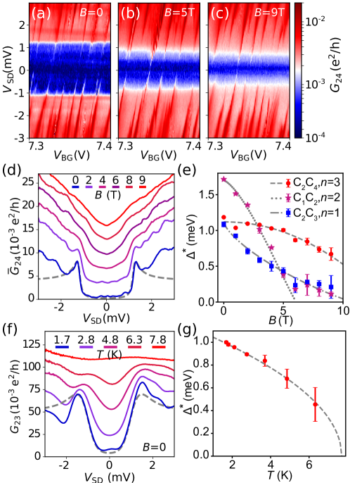
We investigate the gap in the transport characteristics and the field dependence in more detail in Fig. 2 for the same contact pair. Figures 2(a)-(c) show higher resolution conductance maps for a smaller interval, for the magnetic fields , T and T, respectively. The figures show a very clear gap in the conductance map, which is systematically reduced with increasing magnetic field, independently of the sharp resonances. The positions of the latter are unaffected by the gap, so that we can attribute them to resonances in the MoS2, for example due to CB. To extract the energy gap, we plot in Fig. 2(d), averaged over a gate voltage interval of V for each value, for a series of perpendicular magnetic fields. These curves show how the energy gap closes with increasing . The curve at can be fitted well using the model by Blonder, Tinkham and Klapwjik (BTK) 44, including an additional broadening parameter 45, as shown in Fig. 2(d) by a gray dashed line. The fit parameters are consistent with a weakly transmitting barrier in a single N/S junction. At larger fields, the extracted parameters become ambiguous due to a strong broadening of the curves. As a measure for the superconducting energy gap , we therefore plot in Fig. 2(e) the average of the low-bias inflection points of each curve (red dots). For , we find meV, in good agreement with bulk MoRe 26, 39 and one S/N junction dominating the transport. The field dependence of is well described by standard theory of superconductivity for pair breaking impurities in a metal with a mean free path shorter than the superconducting coherence lengths. For the corresponding self-consistency equations we use , with the energy gap in the excitation spectrum and the order parameter determined numerically from for a given pair breaking parameter 46, 47. The latter we interpolate as , with a characteristic exponent. As shown in Fig. 2(e), the best fit we obtain for , meV and the (upper) critical field T. The latter value is clearly larger than reported for bulk MoRe. Seemingly similar data plotted as purple stars and blue rectangles we discuss below.
As expected for a superconducting energy gap, is also reduced with increasing temperature . In Fig. 2(f) we plot as a function of at V for a series of temperatures at in a different cooldown. For the lowest values of , we can reproduce the data using very similar BTK and Dynes parameters as above, only adjusting the normal state resistance and the temperature to K. However, at higher temperatures, the fits become ambiguous, due to a broadening and possibly a temperature dependence of the Schottky barrier 30. Again, we plot the inflection points of the curves as an estimate for , as shown in Fig. 2(g). To determine the critical temperature, we fit the expression and find K and meV, consistent with literature values for bulk MoRe 39, 38.
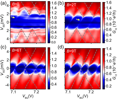
Up to this point, our experiments demonstrate superconducting contacts, but with a weak electronic coupling between the MoS2 and the reservoirs, at least for one contact junction. However, we also find evidence for a stronger coupling of MoS2 regions to the superconductors, relevant for devices relying on the superconducting proximity effect. As an example, we show bias spectroscopy measurements with CB features between contacts C1 and C2 in Fig. 3, for a series of magnetic fields . Similarly as in Fig. 2, we find a transport gap, reduced by larger values. Here, the low-bias ends of the CB diamonds are shifted in energy and in gate voltage, as indicated by the gray dashed lines, consistent with a MoS2 quantum dot (QD) directly coupled to one superconducting contact (i.e. forming an S-QD-N junction) 48. These tips of the CB diamonds are connected across the gap by a single faint resonance, pointed out by yellow arrows, best seen in Fig. 3(b) at T. We attribute these lines to resonant Andreev tunneling 48, in which the electrons of a Cooper pair pass through the QD in a higher order tunneling process. This process is suppressed much stronger by a tunnel barrier than single particle tunneling 49, which suggests that the QD is strongly coupled to the superconductor. At large fields, a quasi-particle background in the superconducting density of states results in single particle CB diamonds 42. With a QD charging energy of meV and using for a disc shaped QD encapsulated in hBN, we estimate the radius of the confined QD region as nm.
The shift of the CB diamonds in gives a measure for 48, which we read out at the bias at which of the large bias conductance is reached at the tip of the CB diamond. The extracted values are plotted as purple stars in Fig. 2(e). Surprisingly, we find a significantly larger zero field gap, meV, and a rather different functional dependence on than for the curves analyzed in Fig. 2 (red dots). The latter is demonstrated by the dotted line obtained for the exponent , and T. In addition, Fig. 2(e) shows a third curve extracted from CB diamond shifts in experiments on another contact pair shown in the supplemental data, Fig. S1. For this curve, we obtain , while meV and T correspond well to the previously obtained values.
While a larger gap in the transport experiments can be simply attributed to a significant fraction of the bias developing across another part of the device, for example across the second N/S junction, the different functional dependence is more difficult to explain. Since nominally the geometry and MoRe film thickness are identical for all contacts, we tentatively attribute this finding to a superconducting proximity region forming in the MoS2 near a strongly couped contact, yielding an induced superconducting energy gap 42, and a different -field dependence of the pair breaking compared to the bulk superconductor.
Additional indications for a stronger coupling to S are the almost gate voltage independent features at , reminiscent of two NS junctions and multiple Andreev reflection processes in between, with a much stronger suppression with increasing than for the observed gap. In the supplemental data, Fig. S2(a), we also show data at higher gate voltages, exhibiting a conductance minimum instead of a maximum at the bias that corresponds to the energy gap, developing into negative differential conductance at the lowest field values. These findings are qualitatively consistent with calculations for an S/I/N/S junction with resonances in the N region 50.
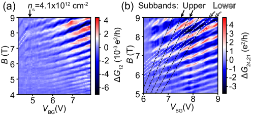
The above data show that our fabrication scheme results in superconducting contacts to monolayer MoS2, possibly with a reasonably strong coupling to the superconductors for some of the contacts. To demonstrate that the intrinsic properties of MoS2 are intact in the bulk crystal, we investigate quantum transport in large magnetic fields and at bias voltages large enough to render the superconducting energy gap irrelevant. In Fig. 4(a) we plot the dc conductance as a function of and , at mV and mK, from which we have subtracted a third order polynomial background for each gate voltage to eliminate effects from the classical Hall effect and CB effects.
Figure 4(a) shows well developed Shubnikov de Haas (SdH) oscillations, suggesting a high quality, with an onset at T. In the Drude model, this onset is interpreted as the charge carriers closing a cyclotron orbit before being scatted, which happens roughly at , with the cyclotron frequency, the effective electron mass, and the scattering time. This yields a lower bound for the carrier mobility of cm2/(Vs), similar to cm2/(Vs) we obtain with Au VIA contacts, identical to the best literature values 24. The discrepancy in mobility between the MoRe and the Au VIA contacts we attribute to heating effects due to the much larger bias we apply to the MoRe contacts to avoid effects of the superconducting energy gap.
The quality of the MoS2 can also be seen in the fact that the the four lowest spin-orbit subbands, corresponding to the valley and the spin degree of freedom, are not mixed by disorder. We find that the slope of the SdH resonances changes by roughly a factor of two at V, corresponding to an electron density of , at which the two upper spin-orbit subbands become populated. Using , we obtain a subband spacing of meV, as reported previously 23. These features prevail also at K, as shown in the supplemental data, Fig. S2(b).
The two-terminal magneto-conductance measurements suffer from large background resistances due to Shottky barriers, which we can partially circumnavigate by performing a three terminal experiment. In Fig. 4(b) we plot the dc conductance , as explained in the figure caption. This technique removes the contact resistance at C4, so that the conductance resonances due to the Landau levels can be measured more clearly. The results in Fig. 4(b) show similar patterns as in better suited Hall bar experiments 23, exhibiting clear superposition patterns of the spin and valley split subbands, indicated by dashed lines. We note that due to the less ideal contact geometry of our devices, we cannot go to lower electron densities in these experiments, because the current density passing near the remote contacts is very low.
In conclusion, we established superconducting contacts to a monolayer of the TMDC semiconductor MoS2 using vertical interconnect access (VIA) contacts, and characterized the superconducting energy gap in different transport regimes. The fact that in most experiments one N/S junction dominates the transport characteristics, and signatures of resonant Andreev tunneling and a superconducting proximity effect, suggest that also contacts with a stronger transmission between the superconductor and the semiconductor are possible, thus opening a path towards semiconductor-superconductor hybrid devices at the limit of miniaturization, with a group of materials - the TMDCs - that offers a very large variety of material properties and physical phenomena.
Associated content
The supplemental data mentioned in the text as Figs. S1 and S2 are available free of charge on the ACS Publications website at DOI:
All data in this publication are available in numerical form at doi.org/10.5281/zenodo.4518683
Acknowledgments
This work was supported financially by the Swiss National Science Foundation project "Two-dimensional semiconductors for superconductor hybrid nanostructures" granted to AB, the Swiss Nanoscience Institute (SNI) project P1701, and the ERC project Top-Supra (787414). K.W. and T.T. acknowledge support from the Elemental Strategy Initiative conducted by the MEXT, Japan, Grant Number JPMXP0112101001, JSPS KAKENHI Grant Numbers JP20H00354 and the CREST (JPMJCR15F3), JST.
References
- Larsen et al. 2015 Larsen, T. W.; Petersson, K. D.; Kuemmeth, F.; Jespersen, T. S.; Krogstrup, P.; Nygård, J.; Marcus, C. M. Semiconductor-nanowire-based superconducting qubit. Phys. Rev. Lett. 2015, 115, 127001
- Leivo et al. 1996 Leivo, M.; Pekola, J.; Averin, D. Efficient Peltier refrigeration by a pair of normal metal/insulator/superconductor junctions. Appl. Phys. Lett. 1996, 68, 1996
- Roddaro et al. 2011 Roddaro, S.; Pescaglini, A.; Ercolani, D.; Sorba, L.; Giazotto, F.; Beltram, F. Hot-electron effects in InAs nanowire Josephson junctions. Nano Research 2011, 4, 259
- Mourik et al. 2012 Mourik, V.; Zuo, K.; Frolov, S. M.; Plissard, S.; Bakkers, E. P.; Kouwenhoven, L. P. Signatures of Majorana fermions in hybrid superconductor-semiconductor nanowire devices. Science 2012, 336, 1003
- Deng et al. 2016 Deng, M.; Vaitiekėnas, S.; Hansen, E. B.; Danon, J.; Leijnse, M.; Flensberg, K.; Nygård, J.; Krogstrup, P.; Marcus, C. M. Majorana bound state in a coupled quantum-dot hybrid-nanowire system. Science 2016, 354, 1557
- Hofstetter et al. 2009 Hofstetter, L.; Csonka, S.; Nygård, J.; Schönenberger, C. Cooper pair splitter realized in a two-quantum-dot Y-junction. Nature 2009, 461, 960
- Hofstetter et al. 2011 Hofstetter, L.; Csonka, S.; Baumgartner, A.; Fülöp, G.; d’Hollosy, S.; Nygård, J.; Schönenberger, C. Finite-bias Cooper pair splitting. Phys. Rev. Lett. 2011, 107, 136801
- Fülöp et al. 2014 Fülöp, G.; d’Hollosy, S.; Baumgartner, A.; Makk, P.; Guzenko, V.; Madsen, M.; Nygård, J.; Schönenberger, C.; Csonka, S. Local electrical tuning of the nonlocal signals in a Cooper pair splitter. Phys. Rev. B 2014, 90, 235412
- Wan et al. 2015 Wan, Z.; Kazakov, A.; Manfra, M. J.; Pfeiffer, L. N.; West, K. W.; Rokhinson, L. P. Induced superconductivity in high-mobility two-dimensional electron gas in gallium arsenide heterostructures. Nat. Commun. 2015, 6, 7426
- Casparis et al. 2018 Casparis, L.; Connolly, M. R.; Kjaergaard, M.; Pearson, N. J.; Kringhøj, A.; Larsen, T. W.; Kuemmeth, F.; Wang, T.; Thomas, C.; Gronin, S., et al. Superconducting gatemon qubit based on a proximitized two-dimensional electron gas. Nat. Nanotechnol. 2018, 13, 915
- Fornieri et al. 2019 Fornieri, A.; Whiticar, A. M.; Setiawan, F.; Portolés, E.; Drachmann, A. C.; Keselman, A.; Gronin, S.; Thomas, C.; Wang, T.; Kallaher, R., et al. Evidence of topological superconductivity in planar Josephson junctions. Nature 2019, 569, 89
- Vischi et al. 2020 Vischi, F.; Carrega, M.; Braggio, A.; Paolucci, F.; Bianco, F.; Roddaro, S.; Giazotto, F. Electron Cooling with Graphene-Insulator-Superconductor Tunnel Junctions for Applications in Fast Bolometry. Phys. Rev. Appl. 2020, 13, 054006
- Graziano et al. 2020 Graziano, G. V.; Lee, J. S.; Pendharkar, M.; Palmstrøm, C. J.; Pribiag, V. S. Transport studies in a gate-tunable three-terminal Josephson junction. Phys. Rev. B 2020, 101, 054510
- Xiao et al. 2012 Xiao, D.; Liu, G.-B.; Feng, W.; Xu, X.; Yao, W. Coupled spin and valley physics in monolayers of MoS 2 and other group-VI dichalcogenides. Phys. Rev. Lett. 2012, 108, 196802
- Bhowal and Satpathy 2020 Bhowal, S.; Satpathy, S. Intrinsic orbital and spin Hall effects in monolayer transition metal dichalcogenides. Phys. Rev. B 2020, 102, 035409
- Žutić et al. 2004 Žutić, I.; Fabian, J.; Sarma, S. D. Spintronics: Fundamentals and applications. Rev. Mod. Phys. 2004, 76, 323
- Wang et al. 2012 Wang, Q. H.; Kalantar-Zadeh, K.; Kis, A.; Coleman, J. N.; Strano, M. S. Electronics and optoelectronics of two-dimensional transition metal dichalcogenides. Nat. Nanotechnol. 2012, 7, 699
- Kormányos et al. 2014 Kormányos, A.; Zólyomi, V.; Drummond, N. D.; Burkard, G. Spin-orbit coupling, quantum dots, and qubits in monolayer transition metal dichalcogenides. Phys. Rev. X 2014, 4, 011034
- Qiu et al. 2013 Qiu, D. Y.; Felipe, H.; Louie, S. G. Optical spectrum of MoS 2: many-body effects and diversity of exciton states. Phys. Rev. Lett. 2013, 111, 216805
- Kormányos et al. 2015 Kormányos, A.; Burkard, G.; Gmitra, M.; Fabian, J.; Zólyomi, V.; Drummond, N. D.; Fal’ko, V. k· p theory for two-dimensional transition metal dichalcogenide semiconductors. 2D Mater. 2015, 2, 022001
- Tang et al. 2017 Tang, S.; Zhang, C.; Wong, D.; Pedramrazi, Z.; Tsai, H.-Z.; Jia, C.; Moritz, B.; Claassen, M.; Ryu, H.; Kahn, S., et al. Quantum spin Hall state in monolayer 1T’-WTe 2. Nat. Phys. 2017, 13, 683
- Miserev et al. 2019 Miserev, D.; Klinovaja, J.; Loss, D. Exchange intervalley scattering and magnetic phase diagram of transition metal dichalcogenide monolayers. Phys. Rev. B 2019, 100, 014428
- Pisoni et al. 2018 Pisoni, R.; Kormányos, A.; Brooks, M.; Lei, Z.; Back, P.; Eich, M.; Overweg, H.; Lee, Y.; Rickhaus, P.; Watanabe, K., et al. Interactions and magnetotransport through spin-valley coupled Landau levels in monolayer MoS 2. Phys. Rev. Lett. 2018, 121, 247701
- Pisoni et al. 2018 Pisoni, R.; Lei, Z.; Back, P.; Eich, M.; Overweg, H.; Lee, Y.; Watanabe, K.; Taniguchi, T.; Ihn, T.; Ensslin, K. Gate-tunable quantum dot in a high quality single layer MoS2 van der Waals heterostructure. Appl. Phys. Lett. 2018, 112, 123101
- Marega et al. 2020 Marega, G. M.; Zhao, Y.; Avsar, A.; Wang, Z.; Tripathi, M.; Radenovic, A.; Kis, A. Logic-in-memory based on an atomically thin semiconductor. Nature 2020, 587, 72–77
- Island et al. 2016 Island, J. O.; Steele, G. A.; van der Zant, H. S.; Castellanos-Gomez, A. Thickness dependent interlayer transport in vertical MoS2 Josephson junctions. 2D Mater. 2016, 3, 031002
- Trainer et al. 2020 Trainer, D. J.; Wang, B.; Bobba, F.; Samuelson, N.; Xi, X.; Zasadzinski, J.; Nieminen, J.; Bansil, A.; Iavarone, M. Proximity-Induced Superconductivity in Monolayer MoS2. ACS nano 2020, 14, 2718
- Costanzo et al. 2016 Costanzo, D.; Jo, S.; Berger, H.; Morpurgo, A. F. Gate-induced superconductivity in atomically thin MoS 2 crystals. Nat. Nanotechnol. 2016, 11, 339
- Roch et al. 2019 Roch, J. G.; Froehlicher, G.; Leisgang, N.; Makk, P.; Watanabe, K.; Taniguchi, T.; Warburton, R. J. Spin-polarized electrons in monolayer MoS 2. Nat. Nanotechnol. 2019, 14, 432
- Cui et al. 2015 Cui, X.; Lee, G.-H.; Kim, Y. D.; Arefe, G.; Huang, P. Y.; Lee, C.-H.; Chenet, D. A.; Zhang, X.; Wang, L.; Ye, F., et al. Multi-terminal transport measurements of MoS 2 using a van der Waals heterostructure device platform. Nat. Nanotechnol. 2015, 10, 534
- Allain et al. 2015 Allain, A.; Kang, J.; Banerjee, K.; Kis, A. Electrical contacts to two-dimensional semiconductors. Nat. Matt. 2015, 14, 1195–1205
- Schauble et al. 2020 Schauble, K.; Zakhidov, D.; Yalon, E.; Deshmukh, S.; Grady, R. W.; Cooley, K. A.; McClellan, C. J.; Vaziri, S.; Passarello, D.; Mohney, S. E.; Toney, M. F.; Sood, A.; Salleo, A.; Pop, E. Uncovering the Effects of Metal Contacts on Monolayer MoS2. ACS Nano 2020, 14, 14798–14808
- Samm et al. 2014 Samm, J.; Gramich, J.; Baumgartner, A.; Weiss, M.; Schönenberger, C. Optimized fabrication and characterization of carbon nanotube spin valves. J. Appl. Phys. 2014, 115, 174309
- Lembke et al. 2015 Lembke, D.; Bertolazzi, S.; Kis, A. Single-layer MoS2 electronics. Acc. Chem. Res. 2015, 48, 100
- Seredinski et al. 2021 Seredinski, A.; Arnault, E.; Costa, V.; Zhao, L.; Larson, T.; Watanabe, K.; Taniguchi, T.; F.Amet,; Newaz, A.; ; Finkelstein, G. One-Dimensional Edge Contact to Encapsulated MoS2 with a Superconductor. arXiv: 2021, 2101.06194
- Telford et al. 2018 Telford, E. J.; Benyamini, A.; Rhodes, D.; Wang, D.; Jung, Y.; Zangiabadi, A.; Watanabe, K.; Taniguchi, T.; Jia, S.; Barmak, K., et al. Via method for lithography free contact and preservation of 2D Mater. Nano Lett. 2018, 18, 1416
- Witcomb and Dew-Hughes 1973 Witcomb, M.; Dew-Hughes, D. The -phase in molybdenum-rhenium; microstructure and superconducting hysteresis. J. Less-Common Met. 1973, 31, 197
- Sundar et al. 2013 Sundar, S.; Sharath Chandra, L.; Sharma, V.; Chattopadhyay, M.; Roy, S. Electrical transport and magnetic properties of superconducting Mo 52 Re 48 alloy. AIP Conference Proceedings. 2013; pp 1092–1093
- Singh et al. 2014 Singh, V.; Schneider, B. H.; Bosman, S. J.; Merkx, E. P.; Steele, G. A. Molybdenum-rhenium alloy based high-Q superconducting microwave resonators. Appl. Phys. Lett. 2014, 105, 222601
- Pillet1 et al. 2010 Pillet1, J.-D.; Quay, C. H. L.; Morfin, P.; Bena, C.; Yeyati, A. L.; Joyez, P. Andreev bound states in supercurrent-carrying carbon nanotubes revealed. Nat. Physics 2010, 6, 965
- Gramich et al. 2017 Gramich, J.; Baumgartner, A.; Schönenberger, C. Andreev bound states probed in three-terminal quantum dots. Phys. Rev. B 2017, 96, 195418
- Jünger et al. 2019 Jünger, C.; Baumgartner, A.; Delagrange, R.; Chevallier, D.; Lehmann, S.; Nilsson, M.; Dick, K. A.; Thelander, C.; Schönenberger, C. Spectroscopy of the superconducting proximity effect in nanowires using integrated quantum dots. Commun. Phys. 2019, 2, 1
- Heedt et al. 2020 Heedt, S.; Quintero-Pérez, M.; Borsoi, F.; Fursina, A.; van Loo, N.; Mazur, G. P.; Nowak, M. P.; Ammerlaan, M.; Li, K.; Korneychuk, S., et al. Shadow-wall lithography of ballistic superconductor-semiconductor quantum devices. arXiv preprint arXiv:2007.14383 2020,
- Blonder et al. 1982 Blonder, G.; Tinkham, M.; Klapwijk, T. Transition from metallic to tunneling regimes in superconducting microconstrictions: Excess current, charge imbalance, and supercurrent conversion. Phys. Rev. B 1982, 25, 4515
- Dynes et al. 1978 Dynes, R.; Narayanamurti, V.; Garno, J. P. Direct measurement of quasiparticle-lifetime broadening in a strong-coupled superconductor. Phys. Rev. Lett. 1978, 41, 1509
- Skalski et al. 1964 Skalski, S.; Betbeder-Matibet, O.; Weiss, P. Properties of Superconducting Alloys Containing Paramagnetic Impurities. Phys. Rev. 1964, 136, A1500
- Gramich et al. 2016 Gramich, J.; Baumgartner, A.; Schönenberger, C. Subgap resonant quasiparticle transport in normal-superconductor quantum dot devices. Appl. Phys. Lett. 2016, 108, 172604
- Gramich et al. 2015 Gramich, J.; Baumgartner, A.; Schönenberger, C. Resonant and inelastic Andreev tunneling observed on a carbon nanotube quantum dot. Phys. Rev. Lett. 2015, 115, 216801
- Sun et al. 1999 Sun, Q.-f.; Wang, J.; Lin, T.-h. Resonant Andreev reflection in a normal-metal–quantum-dot–superconductor system. Phys. Rev. B 1999, 59, 3831
- Zhitlukhina et al. 2016 Zhitlukhina, E.; Devyatov, I.; Egorov, O.; Belogolovskii, M.; Seidel, P. Anomalous inner-gap structure in transport characteristics of superconducting junctions with degraded interfaces. Nanoscale Res. Lett. 2016, 11, 1