Calibration of diamond detectors for dosimetry in beam-loss monitoring
Abstract
Artificially-grown diamond crystals have unique properties that make them suitable as solid-state particle detectors and dosimeters in high-radiation environments. We have been using sensors based on single-crystal diamond grown by chemical vapour deposition for dosimetry and beam-loss monitoring at the SuperKEKB collider. Here we describe the assembly and the suite of test and calibration procedures adopted to characterise the diamond-based detectors of this monitoring system. We report the results obtained on 28 detectors and assess the stability and uniformity of response of these devices.
keywords:
diamond sensor , radiation monitoring , calibration , dosimetry1 Introduction
Natural diamonds, selected for high purity, have been known as good particle detectors with very interesting properties since a rather long time [1, 2]. Practical applications became feasible with the advent of new techniques for the artificial growth of diamond crystals and their steady improvement. Since the initial proposals for applications in high-energy physics experiments [3], the growth process by chemical vapour deposition (CVD) [4] has been progressing towards the production of single-crystals (sCVD) and poly-crystals (pCVD) of larger size, higher purity and reduced variability, at decreasing cost [5]. At present, artificial-diamond applications range from medical micro-dosimetry [6, 7] to beam-condition and beam-loss monitors for high-energy accelerators and experiments: examples include the BaBar experiment at PEP-II (SLAC), CDF at Tevatron (Fermilab), ATLAS and CMS at LHC (CERN) [8, 9, 10, 11].
Diamond is an insulating material due to the large energy gap of about eV between the valence and conduction bands. Diamond sensors, in their simplest planar geometry, are electrically polarised by metal electrodes on two opposite sides, and act as solid-state ionisation chambers. Drifting towards the electrodes, electron-hole pairs created by impinging radiation induce a current in the polarising circuit. Under a quasi-stationary flux of radiation, the induced current is proportional to the energy released by the radiation per unit time, and it can be used to measure the dose rate.
We designed, built, and have been operating a system employing 28 diamond-based detectors for dosimetry and beam-loss monitoring in the interaction region of the SuperKEKB electron-positron collider for the Belle II experiment [12, 13]. The main requirements for these detectors are: a wide range of radiation dose-rates, from a few to several hundred , and performance stability in locations where an integrated dose in excess of 10 Mrad can be expected through the lifetime of the experiment. Reference [14] details the performance of this monitoring system during the first two years of SuperKEKB operations.
In this paper, we report on mechanical assembly, test and calibration procedures of the diamond detectors employed in such a system, aiming at a comparative assessment of their performance for our radiation-monitoring purposes.
2 Detector assembly and dark currents
After carrying out some preliminary studies to compare the response of pCVD and sCVD diamond sensors equipped with electrodes of different materials, we opted for sCVD diamonds from Element Six [15] with electrodes processed by CIVIDEC [16]. The specifications of the supplied sensors are: sCVD diamond with mm2 faces and mm thickness, with a tolerance of / mm and mm for the lateral dimensions and the thickness, respectively; mm2 electrodes on both faces, made of Ti+Pt+Au layers with ++ nm thickness.
The sensors passed the following quality controls before delivery by CIVIDEC: (i) maximum dark current within pA in the bias-voltage range V, and within pA in the range V; (ii) average ionisation-energy less than eV and regular pulse shape from a measurement with particles from 241Am decays; (iii) stable current through one-hour irradiation with electrons from 90Sr decays, with bias voltages of V and V; (iv) visual inspection and rejection in case of deep scratches.
We mounted each diamond sensor in a ceramic-like Rogers printed-circuit board (PCB) [17], as shown in Figure 1.
We first soldered the inner conductors of two miniature coaxial cables, each m long, to the printed board pads, while we used conductive glue to mechanically fix the cables and establish the connection of their outer conductors with the outer shielding of the printed-circuit board. This solution is mechanically more reliable (less prone to breaking of the cable shield following repeated bending) with respect to soldering the outer conductors of the coaxial cables to the package. The cable length was determined by constraints imposed by their use in the Belle II setup.
After cleaning the PCB-cables ensemble by isopropyl alcohol, using conductive glue we attached the diamond sensor to a square pad that connects the back-side electrode to the soldering pad of one of the coaxial cables. Finally, we connected the front-side electrode of the sensor to the soldering pad of the other cable by two ball-bonded gold wires. After the measurements presented in Sect. 3.1, we completed the mechanical and electrical shielding by gluing a thin (m) aluminium cover on the front side of the package.
We performed preliminary measurements of dark current versus bias voltage on all detectors as a quality control of the assembly process. We connected the diamond detectors to the measuring instrument via the miniature coaxial cables and, while keeping them in the dark, we scanned the bias voltage up to V. Although we observed fairly large variations among different detectors, memory effects and long stabilization times, in all cases the measured dark current was less than about 10 pA at V and not larger than about pA at V.
3 Detector calibration
The response of diamond sensors as dosimeters is not expected to be uniform. Crystal imperfections from the CVD-growing process can trap or recombine charge carriers generated by irradiation. Such imperfections differ from crystal to crystal, yielding non-uniform charge-collection efficiency at a given bias voltage. Properties of the diamond-electrode interface are also sensor-dependent. Some detectors might feature non-blocking electrodes, which inject charge into the diamond bulk, and, in conditions that support the so-called photo-conductive gain, the charge-collection efficiency might even exceed unity [18, 19].
For these reasons, an individual calibration of each detector is needed in order to relate the measured current to a dose rate. Before the calibration, detailed in Sect. 3.3, we carried out two sets of measurements on each detector. The first set aimed at checking the transport properties of the charge carriers and the average ionisation energy to create an electron-hole pair. With this study, reported in Sect. 3.1, we got an understanding of the homogeneity of the sensor properties within our sample. In the second set of measurements, we determined the suitable bias voltage for operating the sensors and checked the stability of the output current generated by irradiation. This study is presented in Sect. 3.2.
3.1 Measurement of the charge-carrier properties
To study the transport properties of electrons and holes, we used the transient-current technique (TCT) [20], which in our application employs monochromatic particles to generate electron-hole pairs localised at a small depth in the diamond bulk, very close to one electrode. Depending on the bias polarity, charge carriers of one type are readily collected at the nearby electrode, while the others drift to the opposite electrode along the electric-field lines, inducing a current pulse. Information on the transport properties of the drifting carriers is determined by the features of this pulse: its shape is related to the carriers lifetime and to the uniformity of the electric field in the diamond bulk; its duration is related to the drift time of the selected carriers; its integral to the collected charge.
To carry out the TCT measurements, we used a -kBq 241Am source of particles, emitted with MeV energy on average. The diamond detectors, assembled on their PCB package but without the aluminium cover, so that the particles could reach the detector surface, were inserted in an aluminium support. This support provided appropriate shielding and allowed to position the source at repeatable distance ( mm) from the front electrode of the diamond sensor, centered with respect to it. The particles were collimated by a Plexiglas insert, 2 mm thick, with a circular hole of 1 mm diameter, so that they would hit the sensor well within the electrode area, in a region where edge effects on the electric field can be neglected. A scheme of the setup is shown in Figure 2.
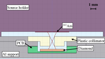
From a detailed simulation of this setup based on the FLUKA software [21], we estimated that an particle releases in the diamond crystal of its energy, corresponding to MeV on average; only is released in the metallic electrode, while the rest is distributed between air and the collimating structure. The penetration depth in the diamond crystal is limited to about m.
We connected a high-voltage supply, delivering up to V, to the back-side electrode of the diamond detector via a Bias-T circuit [22] that, although not needed to decouple the signal from the DC bias, has proven effective in suppressing the noise. We connected the front electrode directly to the input of a voltage amplifier with 3 GHz band-width, 53 dB gain and 50 input impedance (AM-02A from Particulars [22]). The output of the amplifier was analyzed by a digital storage oscilloscope.
We optimised this experimental setup after a first set of measurements on a sub-sample of detectors, made with a less effective collimator, allowing the particles to hit the whole detector area (including the edges) with a wide range of incidence angles. In that first setup, we had also used a different readout scheme, yielding larger signal attenuation from cables and the Bias-T. Those differences have a negligible impact in the analysis of the charge-carrier transport, but significantly affect the estimated ionisation energy. We report the results obtained with the optimised setup and note the distinction from the old configuration only when it is relevant.
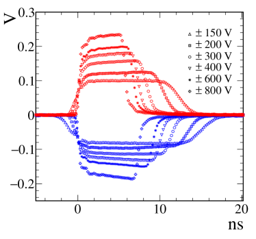
We analysed the signal generated by the particles for twelve choices of the bias voltage between V. We discarded measurements with bias voltage between V, because the trigger level of the oscilloscope, kept above noise, biased the measurement for lower pulses. Figure 3 reports the time development of the average of 1000 signal pulses from a diamond detector. Each measurement provides the average pulse-integral and the average pulse-width at half height . We assumed a uniform electric field in the diamond bulk (as suggested by the approximately flat top of the signal shapes) and a drift distance of the carriers equal to the sensor thickness mm. For each value of the electric-field intensity , we estimated the drift velocity and the mobility for both drifting carriers.
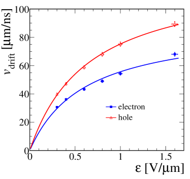
We empirically described the drift velocity as a function of by the following expression [20]:
| (1) |
where is the mobility extrapolated to low field-intensity, and is the saturation velocity at high field. Figure 4 shows an example of as a function of with a fit of the data using Eq. (1). The values of and obtained by fitting Eq. (1), averaged over our sample of diamond detectors, are: and for holes, and for electrons. The standard deviation of these results is about , confirming that the transport properties of charge carriers are sufficiently homogeneous. We did not observe significant differences between the results obtained with the optimised and non-optimised setup.
For each pulse integral measured by the oscilloscope, we estimated the collected charge as , where and are the input impedance and the measured gain of the amplifier, respectively. Independently of the setup used, we observe that the estimated collected charge versus applied voltage saturates to an approximately constant value. The fractional difference between the collected charge evaluated from drifting electrons or holes does not exceed .
From the collected charge , we determined the average ionisation energy for electron-hole pairs as
| (2) |
where is the average energy released in diamond by the particles and is the charge of the electron. We computed the energy from a detailed simulation of the source, the collimator, and the sensor with its support. We did not simulate the charge-carrier transport and we assumed a full charge-collection efficiency. We obtain an average value eV and eV with the optimised and non-optimised setup, respectively. The results obtained with the non-optimised setup are understood to originate from a biased estimation of the collected charge, due to attenuation in circuit components, to long tails in the shape of the signals, and a contamination of about 10% of signals with irregular shape, caused by a poor collimation of the particles. Taking into account those biases, all values are consistent within 5% with an average value of eV, which is usually quoted in literature for high-quality diamond sensors [23].
3.2 Current-voltage profiles under irradiation and current stability
A stable and reproducible response to radiation is crucial for dosimetry and monitoring. The detector response might depend on the applied bias voltage, and the optimal operation value has to be determined. We obtained this by measuring the current-voltage (-) profile under irradiation for each detector after the full assembly (i.e. after gluing the aluminium cover on the PCB package).
We measured the current over a V bias-voltage range. We irradiated the detectors for 2–5 minutes for each value of the bias voltage. The radiation was provided by a steady flux of electrons from the source described in Sect. 3.3, using the same setup detailed therein. We placed the source at a fixed distance, which ranged from about mm to mm from the detector, yielding currents typically between 1–2 nA at V bias.
Figure 5 shows some examples of the - profiles obtained from three sensors exhibiting different behaviour. Plot (a) represents the situation typical for about a half of our sensors, which display a symmetric - characteristic. In these cases, the current reaches a plateau for between – V, remaining approximately flat up to V. Plots 5 (c) and (d) are examples of - profiles characterising the remaining sensors, where an asymmetric response is observed. For one polarity the current reaches a constant value for typically greater than V, while for the opposite polarity no current saturation is observed.
For those detectors with an asymmetric - profile, the response can also present an hysteresis: the current value measured at a given voltage depends on the direction of the voltage scan, indicating that the current is not a function of alone, but depends also on the previous “hystory”. The variation of the current due to such hysteresis effects is not significant at V for the bias polarity showing the plateau, although it can be much larger in the opposite polarity.
We cannot provide a clear explanation for the asymmetric - profiles and the hysteresis effects; possible hypotheses range from a crystal asymmetry from the growth process to features of the diamond-electrode interface. For these sensors we decided to adopt the voltage polarity leading to a saturation of the current.
For a couple of sensors, we also sampled the region – V in finer steps, to study in more detail the onset of charge-collection efficiency. An example is shown in Figure 5 (b). With a bias voltage as small as V, the measured current is about 50% of the plateau value. The charge-collection efficiency rises very steeply within a couple of volt, and slowly saturates increasing the bias.
We chose V as the optimal operation voltage (with the sign set for each sensor, according to the - profiles). With this choice, our detectors have a (steady-state) charge-collection efficiency close to 100% on average.
We checked the stability in time of the radiation-induced current at the chosen operation voltage, over a time span ranging from several hours to a few days. Figure 6 reports a few typical examples. On the sensors exhibiting symmetric - profiles, we observed a very stable response over time with values constant within . For those with asymmetric - profiles, we observed constant current values for the best polarity, with fluctuations no larger than 5%. We noticed larger instabilities, also with random spikes, for the opposite polarity. These stability tests confirmed our choice of the best polarity for the sensor with asymmetric - profile.
We also observed a different time response between the sensors. Although all detectors react within 1 s (time-resolution of the current sampling in these measurements) from the start of the irradiation, some of them present a two-step response: about 90% of the value of the current is reached within 1 s, followed by a slower transient to 100% with time duration ranging from tens of seconds to many minutes. We attribute this behaviour to different amounts of crystal defects, corresponding to trapping and de-trapping effects of the charge carriers following irradiation transients [24].
3.3 Current-to-dose calibration factors
To employ the diamond detector as a dosimeter, we need to relate the current measured under irradiation to a dose rate. We define a calibration factor , such that
| (3) |
where is the dose rate, i.e. the energy per unit time released by the radiation in the detector mass , and is the measured current.
To account for non-uniform response of our detectors, we split into two terms, as
| (4) |
where is a constant factor that takes the value
| (5) |
considering the mass of our detectors mg and an average ionisation energy to create electron-hole pairs eV. The factor is a dimensionless constant characteristic of each detector. A value would represent (i) a fully efficient detector, (ii) with blocking electrodes, and (iii) ionisation energy of 13 eV. Any deviation from unity is a measurement of the departure from the assumptions (i)–(iii). We notice that assumption (ii) implies no amplification factor from the “photoconductive gain” process [18, 19].
To determine the value of , we used a silicon diode as a reference. We exposed the diamond detectors and the diode to a source of radiation, and we determined the ratio of the signal current from the diamond detector to the reference current from the diode. We obtain the characteristic constant by comparing the measured signal/reference current ratio and that expected from a detailed simulation of the experimental setup, where we adopt the hypotheses (i)–(iii) for the diamond detectors and we assume a good knowledge of the diode response. The use of a reference greatly reduces uncertainties associated to the source activity and to the simulation of the setup, that would otherwise limit the accuracy of the calibration procedure.
3.3.1 Measurement of signal-to-reference ratio of currents
We exposed the diamond detectors to a steady flux of electrons emitted by a 90Sr radioactive source. We moved the source along a straight line orthogonal to the detector surface and traversing its center, and changed the source-detector using a stepper motor driven by an Arduino micro-controller [25]. The origin is known with an accuracy of mm.
The source consists of an ion-exchange organic spherical bead, mm in diameter, with radioactive nuclei uniformly distributed in the volume. The bead is mounted on top of a steel needle embedded in a Plexiglas container. Electrons are emitted isotropically from the decays and , with a known energy spectrum up to about MeV. Being the 90Y half-life much shorter than that of 90Sr, the 90Y decay rate is in equilibrium with its production rate. Thus, the rate of electrons emitted from the source is twice the 90Sr activity. At the time of these measurements, the activity of the source from the 90Sr decays was approximately 3 MBq.
We connected the detector to a bias-voltage supply [26] and to a pico-ammeter [27] which measured the signal current. We interfaced the stepper motor, the voltage source, and the pico-ammeter to a computer to automatically perform complete sequences of measurements. We explored a range of source-detector distance from mm to mm and for each distance we recorded the signal current , averaging million readings taken in 2 minutes. An example is shown in Figure 7.
We used the same setup and procedure to measure the reference current from the silicon diode. The diode features an n bulk, a p+ layer obtained by Boron ion implantation, and a n+ layer for the ohmic contact. The square-shaped diode, fabricated on a substrate mm2 wide and mm thick, is hosted in a package similar to that of the diamond detectors. The diode is closely surrounded by a p+ guard ring which delimits the charge collection volume of the central diode, given by an effective area of mm2 and the depletion thickness. We applied a 100 V bias to the n+ contact, with the p+ layer and connected the guard ring to ground. In this condition, the diode was overdepleted with an active volume given by the diode effective area and the substrate thickness.
While for diamond detectors the dark current was negligible, it contributed significantly in the measurements with the diode, especially at far source-detector distance. Thus, each time we changed the distance, we monitored the dark current, and we subtracted its value from the current measured under irradiation. The dark current was constant at about nA. The reference current from the diode measured as a function of is shown in Figure 7.
Both signal and reference currents are roughly proportional to , as expected from the variation of the -electron flux on the detector surface as a function of , for an almost-pointlike source. The signal-to-reference ratio of currents,
| (6) |
is constant versus , as shown in the Figure 7 (b). The flatness of denotes that the measured values of the source-detector distance are compatible in the two sets of data.
3.3.2 Computation of the expected ratio of currents
We computed the expected signal (reference) current () from the energy released per electron in the detector volume, (). We used the FLUKA software [21] to obtain the released energy, by implementing a realistic and detailed model of the full setup, from the spherical source to the detectors, with all supports and packaging, to account for the full geometry and all materials traversed by the radiation.
We did not attempt to model the charge-carrier generation and transport. We used a simplified model where all energy released in the active volume generates charge carriers. For the diamond detector, we used assumptions (i)–(iii) presented in Sect. 3.3; for the diode, we assumed an average ionisation energy eV [28] and a full charge-carrier collection efficiency. In this model, the expected current is expressed as
| (7) |
where the presence of the index “r” identifies the reference-diode quantities; is the charge of the electron; and is the activity, with the factor to account for the electrons emitted from and decays.
The dependence on the source activity cancels out in the ratio of expected currents,
| (8) |
which is constant as a function of . This ratio is shown in Figure 7 (b), where it is compared with the ratio measured from a diamond detector. The expected and measured values are very close to each other.
3.3.3 Calibration factors: results
We determine the characteristic constant for each detector from the ratio
| (9) |
where we assume a precise modelling of the silicon diode (i.e. ).
The distribution of is shown in Figure 8 (a). The mean value is , which corresponds on average to fully-efficient detectors, with uniform good-quality crystal ( eV) and blocking electrodes (unitary photoconductive gain). Maximum deviations from this ideal behaviour are limited to about 50%.
From the measured we obtain the calibration factors reported in Figure 8 (b). On average, the dose rate is about for a measured current of nA. The statistical uncertainty on each value of is negligible with respect to the systematic uncertainty, which is detailed in the next section.
3.3.4 Systematic uncertainties
The relative uncertainty on each calibration factor totals from the contributions summarised in Table 1 and described as follows.
| Systematic-uncertainty source | |
|---|---|
| [%] | |
| Current transients and fluctuations | |
| Measurement of source-detector distance | |
| Silicon ionisation energy | |
| Silicon-diode volume | |
| Package shielding (diode) | |
| Package shielding (diamond detectors) | |
| Simulation approximations and statistic | |
| Source description | |
| Total |
The largest source of uncertainty is due to possible variations of the signal current due to a transient time to reach a stable value. As discussed in Sect. 3.2 most detectors reached a stable output value within a second from the start of irradiation, with small fluctuations below 1% under steady irradiation. Some other detectors showed a longer transient time, where the initial values of the current is smaller by approximately 5% than that reached after a certain period of steady irradiation. To account for the different response of the detectors to sudden changes of irradiation conditions, which are expected to occur in the SuperKEKB interaction region, we associate a systematic uncertainty of to the measurement of the current, which is propagated to the calibration factor.
The measured values of are expected to be constant as a function of , and any trend versus can be ascribed to a different offset in the source-detector distance between the measurement with the diamond detector and the diode. We observed constant values of versus with a maximum variation of 2% for some detectors, after correcting the distance with a detector-dependent offset, that averages mm. Without the offset correction, the deviation from flatness are larger than 2%, and the average value of changes by . We assign this change as a systematic uncertainty.
A major source of uncertainty is related to the reference diode, as we assumed a perfect modelling of its response to obtain . The estimated current from the diode depends on the ionisation energy, on the charge-collection efficiency, and on the energy released in the active volume.
We propagate to the uncertainty of eV on the ionisation energy; this contributes a relative systematic uncertainty of .
We assumed a fully efficient diode in collecting all generated charge at V bias. This assumption is supported by - measurements under irradiation on the diode, and we consider the uncertainty on this assumption to be negligible.
The released energy is proportional to the active volume of the diode used in the simulation, which is known within the uncertainties of the surface and thickness of the detector. To assess a systematic uncertainty on , we make two variations, by changing the active surface and the depletion thickness by and m, respectively, which are the associated uncertainties. These variations corresponds to a minimum and a maximum active volume. For both cases, we compute the released energies as a function of the source-detector distance, and the resulting expected ratio from Eq. (8). We take the difference between each new value of and its nominal value, and we consider the largest difference to assign a relative uncertainty . This is propagated to and contributes 4% to the systematic uncertainty.
In a similar manner, we compute the contribution associated to the uncertainty on the thickness of the aluminium packaging that impacts the released energy. We vary in simulation the thickness of the aluminium cover by m, which is the uncertainty associated to the cover used in the diode packaging. Other sources that affect the released energy, such as a 0.1 m layer of silicon oxide on the surface (the diode area is metallized only around the edge), are considered negligible.
The value of depends also on the ionisation energy of the diamond detector, on the released energy inside its active volume, and on its charge-collection efficiency. Departures of all these factors from the values assumed in the calculation of the estimated current are accounted for by the characteristic constant . We notice that any variation on due to an uncertainty on the value of the ionisation energy, or that on the detector volume, are counterbalanced by a variation of in the definition of in Eq. (4). Therefore, we do not compute a systematic uncertainty for these two sources.
The aluminium packaging affects the estimation of the released energy in the diamond detectors in a similar fashion as for the diode, and the impact from the uncertainty on its thickness is computed with the same procedure. We consider an uncertainty of m on the thickness in this case, to account for the different individual covers of the diamond detectors. The resulting systematic uncertainty is . We consider other sources that affect the released energy, e.g. the uncertainty on the volume of the electrodes of the diamond detectors, to be negligible.
As for what concerns the charge-collection efficiency, a departure from the assumed value of 100% is included in the characteristic constant measured for each detector. A possible source of uncertainty is due to small fluctuations of the voltage provided by the power supply, which presented variations of . From the - results presented in Sect. 3.2, we expect only sub-percent changes of the efficiency for V variation around a V bias. Therefore, we consider negligible the associated systematic uncertainty on .
The statistical uncertainty from the size of the simulated samples contributes a negligible uncertainty too. Uncertainties related to other assumptions entering the simulation, such as the transport model used in FLUKA for the electrons, are found to be smaller than , as these contributions are greatly reduced in the ratio of Eq. (8). For the same reason, an imprecise modelling of the source (material, density, fraction of radioactive nuclei) contributes only a sub- systematic uncertainty.
3.3.5 Additional checks
By using the silicon diode as a reference, we do not need the value of the source activity to determine . Alternatively, the source activity can be measured with the silicon diode through Eq. (7). In this case, we find an activity of about MBq, to be compared with a nominal value of approximately MBq. We notice that the uncertainty on the nominal activity is not precisely known, and it could be as large as .
If we were to use the nominal activity, would be computed by the ratio of the current measured from the diamond detector and that computed from Eq. (7). In this case, the mean values of would be about . Such a value would be explained either by an ionisation energy of about 20 eV, in disagreement with the TCT measurements reported in Sect. 3.1, or by a photoconductive gain around for a V bias, in disagreement with - measurements reported in Sect. 3.2. This would suggest either a large uncertainty on the nominal activity, or a bias on the simulation of the experimental setup, which is greatly reduced in our method by using the diode as a reference through Eq. (8).
For two detectors, we also carried out two checks of the value of using photons as a source of radiation.
In the first check, we exploited soft photons, with a known energy spectrum averaging about 15 keV, provided by a small X-ray tube [29]. We measured the signal-to-reference ratio of currents at a fixed source-detector distance, using the same silicon diode employed in the measurement with the source. The X-ray flux yielded currents between nA and nA. We compared the measured ratio with that estimated by means of a full simulation through FLUKA, to obtain from Eq. 9. We found values of in agreement with those obtained with the radiation.
With the second check, we aimed at exploring dose rates much higher than those provided by the source. We used a source of rays from 60Co decays, with energies of MeV and MeV, available at ISOF-CNR in Bologna. The source (Gammacell 220) has a certified dosimetry performed with alanine dosimeters in 2007 by Risø National Laboratory. We measured dose rates with the calibrated diamond detectors in agreement with the certified values, scaled by the 60Co reduced activity at the time of the test due to radiative decay. We observed a very good linear dependence between the measured currents and the dose rates, spanning a range between nA and nA corresponding to dose rates between and . This builds confidence on the validity of the measured calibration factors over a range spanning from tens of to some .
4 Conclusions
We chose sensors based on single-crystal diamond as dosimeters for a beam-loss monitor at the SuperKEKB electron-positron collider. The diamond crystals, grown by the chemical vapour deposition, are equipped with Ti+Pt+Au electrodes and assembled in dedicated packages. We presented the test and characterisation of a sample of 28 sensors.
We found that charge-carrier properties and average ionisation energies, as measured by the transient-current technique, are sufficiently homogeneous across the set of sensors for our purpose. For about a half of our detectors, we observed hysteresis effects and unstable currents under constant irradiation for bias voltages of a specific polarity; stable and reproducible values of the current for the opposite polarity. The other half of the sensors exhibit a symmetric response with respect to bias voltage polarity. We determined the best polarity for each detector, and we found the optimal bias voltage to be V, for which we observed a charge-collection efficiency close to 100%.
We determined the current-to-dose-rate calibration factors by irradiating the sensors with electrons from 90Sr decays, and by comparing the measured current with that expected from a simulation, used to estimate the dose rate due to the irradiation. We employed a silicon diode, irradiated under same conditions, as a reference in order to greatly reduce uncertainties related to the -source activity and to the simulation, that would otherwise spoil the accuracy of the calibration. We obtained detector-dependent calibration factors with a relative uncertainty of 8%. We validated the calibration factors with X and radiation for dose-rate spanning a range from tens of to some .
The monitor system based on these detectors has been proving crucial for running the Belle II experiment in safe conditions during the last two years [14], while beam-background radiation has been continuously evolving with the progress of the SuperKEKB collider towards unprecedented values of luminosity. The test and calibration procedures reported here represent valuable resources for the preparation of eight new diamond detectors that will be installed with an upgrade of the Belle II silicon vertex detector in 2022.
Acknowledgements
This research was supported by Istituto Nazionale di Fisica Nucleare (INFN) in the framework of the Belle II experiment. Motivation for improving our calibration procedures was enhanced by useful discussions with SuperKEKB and Belle II colleagues. We gratefully acknowledge the contribution of Francesco Di Capua (University Federico II and INFN Naples, Italy) in setting up measurements with the 60Co source.
References
- [1] S. F. Kozlov, et al., Preparation and characteristics of natural diamond nuclear radiation detectors, IEEE Transactions on Nuclear Science 22 (1) (1975) 160–170.
- [2] C. Canali, et al., Electrical properties and performances of natural diamond nuclear radiation detectors, Nuclear Instruments and Methods 160 (1) (1979) 73 – 77.
- [3] M. Franklin, et al., Development of diamond radiation detectors for SSC and LHC, Nuclear Instruments and Methods in Physics Research Section A: Accelerators, Spectrometers, Detectors and Associated Equipment 315 (1) (1992) 39 – 42.
- [4] J. C. Angus, et al., Growth of diamond deed crystals by vapor deposition, Journal of Applied Physics 39 (6) (1968) 2915–2922.
- [5] R. S. Sussmann, CVD Diamond for Electronic Devices and Sensors, John Wiley & Sons Ltd, 2009.
- [6] J. A. Davis, et al., Evolution of diamond based microdosimetry, Journal of Physics: Conference Series 1154 (2019) 012007.
- [7] C. Verona, et al., Toward the use of single crystal diamond based detector for ion-beam therapy microdosimetry, Radiation Measurements 110 (2018) 25 – 31.
- [8] A. J. Edwards, et al., Radiation monitoring with CVD diamonds in BaBar, Nucl. Instrum. Meth. A 552 (2005) 176–182.
- [9] R. Eusebi, et al., A diamond-based beam condition monitor for the CDF experiment, in: 2006 IEEE Nuclear Science Symposium Conference Record, Vol. 2, 2006, pp. 709–712.
- [10] V. Cindro, et al., The ATLAS beam conditions monitor, JINST 3 (2008) P02004.
- [11] R. Hall-Wilton, et al., Fast beam conditions monitor (BCM1F) for CMS, in: 2008 IEEE Nuclear Science Symposium Conference Record, 2008, pp. 3298–3301.
- [12] Y. Ohnishi, et al., Accelerator design at SuperKEKB, PTEP 2013 (2013) 03A011.
- [13] T. Abe, et al., Belle II Technical Design Report arXiv:1011.0352.
- [14] S. Bacher, et al., Performance of the diamond-based beam-loss monitor system of Belle II, Nucl. Instrum. Meth. A 997 (2021) 165157.
- [15] Element Six (UK) Ltd., http://www.e6.com/.
- [16] CIVIDEC Instrumentation GmbH, https://cividec.at/.
- [17] Rogers Corporation: http://www.rogerscorp.com/.
- [18] A. Rose, Concepts in photoconductivity and allied problems, Interscience Publishers, 1963.
- [19] K.-C. Kao, Dielectric phenomena in solids with emphasis on physical concepts of electronic processes. Chapter 7: electrical conduction and photoconduction, Elsevier Academic Press, 2004.
- [20] H. Pernegger, et al., Charge-carrier properties in synthetic single-crystal diamond measured with the transient-current technique, Journal of Applied Physics 97 (7) (2005) 073704.
- [21] A. Ferrari, P. R. Sala, A. Fassò, J. Ranft, FLUKA: a multi-particle transport code (program version 2005), CERN Yellow Reports: Monographs, CERN, Geneva, 2005.
- [22] Particulars: http://www.particulars.si/.
- [23] E. Berdermann, Diamond for particle and photon detection in extreme conditions, Comprehensive Hard Materials 3 (2014) 407–467.
- [24] P. Bergonzo, et al., Improving diamond detectors: a device case, Diamond and Related Materials 16 (4) (2007) 1038 – 1043, proceedings of Diamond 2006, the 17th European Conference on Diamond, Diamond-Like Materials, Carbon Nanotubes, Nitrides and Silicon Carbide.
- [25] Arduino: https://www.arduino.cc.
- [26] CAEN DT5521HM high voltage supply, CAEN: http://www.caen.it.
- [27] AH501 pico-ammeter: http://ilo.elettra.trieste.it/.
- [28] F. Scholze, H. Rabus, G. Ulm, Mean energy required to produce an electron-hole pair in silicon for photons of energies between 50 and 1500 eV, Journal of Applied Physics 84 (5) (1998) 2926–2939.
-
[29]
A. Gabrielli, In-depth
characterization and optimization of diamond sensors for an update of the
Belle 2 monitor system, Laurea thesis, Trieste U.,
BELLE2-MTHESIS-2020-008, (2020).
URL https://docs.belle2.org/record/2151