Precise, Subnanosecond, and High-Voltage Switching of Complex Loads Enabled by Gallium Nitride Electronics
Abstract
In this work, we report the use of commercial Gallium Nitride (GaN) power electronics to precisely switch complex distributed loads, such as electron lenses and deflectors, without impedance matching. Depending on the chosen GaN field effect transistor (GaNFET) and driver, these GaN pulsers are capable of generating pulses ranging from 100 - 650 V and 5 - 60 A in 0.25 - 8 ns using simple designs with easy control, few-nanosecond propagation delays, and MHz repetition rates. We experimentally demonstrate a simple 250 ps, 100 V pulser measured by a directly coupled 2 GHz oscilloscope. By introducing resistive dampening, we can eliminate ringing to allow for precise 100 V transitions that complete a -10 V to -90 V transition in 1.5 ns, limited primarily by the inductance of the oscilloscope measurement path. The performance of the pulser attached to various load structures is simulated, demonstrating the possibility of even faster switching of internal fields in these loads. These circuits also have active regions and under 1 W power dissipation, enabling their integration into a wide variety of environments and apparatus. The proximity of the GaNFETs to the load due to this integration minimizes parasitic quantities that slow switching as well as remove the need to match from lines by allowing for a lumped element approximation small loads. We expect these GaN pulsers to have broad application in fields such as optics, nuclear sciences, charged particle optics, and atomic physics that require nanosecond, high-voltage transitions.
I Introduction
Nanosecond, high-voltage pulses have broad application in in the physical sciences, ranging from their use in optics for driving Pockels cells and piezoelectric actuators Bishop and Barker (2006), to their use in deflecting and gating electrons or ions in nuclear science, spectroscopy Wolff and Stephens (1953), charged particle optics Zhang et al. (2020); Zajfman et al. (1997), and quantum measurement schemes Kruit et al. (2016). In the past, these fast pulses have been generated by a wide variety of technologies such as silicon power FETs Jiang (2007); Chaney and Sundararajan (2004); Baker and Johnson (1992), avalanche transistor circuits Jinyuan, Bing, and Zenghu (1998); Henebry (1961); Benzel and Pocha (1985), step recovery diodes Zou, Gupta, and Caloz (2017), non-linear transmission lines Afshari and Hajimiri (2005), spark gaps Carl E. Baum, Carin, and Stone , and laser-triggered semiconductor gaps Mourou and Knox (1979); Kohler et al. (2013). Various reviews and studies exist comparing some of these techniques De Angelis et al. (2011); Martin (1992); Mankowski and Kristiansen (2000), and most recently the use of nanoplasmas Samizadeh Nikoo et al. (2020) has given record switching performance. While some techniques deliver pulses greater than 100 kV in < 100 ps, these approaches have varied trade-offs and shortcomings. Among the most important are the cost and complexity of pulser designs, their large size and high power dissipation that force us place pulsers far away from the loads they drive, the lack of simple, single-shot driving schemes, and slow repetition rates. All of these techniques also have problems with ringing due to resonances in the pulse generating circuits and loads, and impedance mismatch problems developed over the length scales of the transmission line and loads. For structures that requires precise switching, removing ringing requires either slowing of the pulse edge with low pass filtering to avoid load resonances, the use of resonant filters to selectively remove those worst resonances, or predistortion calibration techniques that require high bandwidth arbitrary waveform generators to create messy pulses that result in clean output switching Klopfer et al. (2020).
In this work, we demonstrate the potential of simple and low-cost GaN power electronics for fast and precise high-voltage switching. While such electronics have been used extensively for high-efficiency power converters Wu et al. (2008), amplifiers Brown et al. (2011), and pulsed lasers Glaser (2018), we believe that these circuits have the potential for wide application in physics and engineering for high power nanosecond switching. These circuits are fast and simple to control, with single-shot pulsing triggered by a 5 V logic inputs up to a repetition rate of 60 MHz and propagation delays of a few nanoseconds. The high power efficiency and low thermal dissipation of these circuits also offer advantages in operation, leading to small form factors that are compatible with vacuum environments common in physics applications. They are also inexpensive, costing two orders-of-magnitude less than equivalent commercial pulsers. Through careful selection of parts and layout optimization, the reported pulser achieves both undamped 250 ps and damped 1.5 ns, 100 V transitions (as measured by the time to go from -10 V to -90 V, or 10% to 90%) into a 2 GHz oscilloscope. These measurements are limited primarily by the path inductance into the oscilloscope. We then simulate the response of various predominantly inductive, capacitive, and mixed loads to the GaNFET pulser, demonstrating precise nanosecond transitions even faster than those we measured experimentally, with ringing controlled to within 1% the transition amplitude by resistive damping. We discuss alternative topologies allowing for symmetric pulse edges and higher voltage operation. Finally we discuss how our GaNFET-based switching performance in real loads compares to that of low-pass filtered pulses on lines.
II Experimental Validation
Wide bandgap semiconductors have long been considered excellent candidates for power electronics due to their ability to withstand voltage and currents far beyond that of silicon, low channel resistances, and high temperature compatibility Amano et al. (2018). In recent years, GaN on silicon technology has emerged as a low cost and robust option with commercial products that have small gate and output capacitances, optimized packages with minimal parasitic inductances, and a wide variety of current and voltage ratings Lidow et al. (2019). Along with these advances, commercial drivers with subnanosecond rise times, 7 A of peak drive current, 60 MHz repetition rates, and 2.5 ns propagation delays have emerged Instruments (2018). Together, these offer the possibility of subnanosecond switching of hundreds of volts and tens of amperes.
In order to validate these switching speeds, we built a testing circuit from the LMG1020 driver from Texas Instruments along with the 200 V EPC2012C enhancement mode GaNFET from the Efficient Power Corporation. The basic circuit design is shown in Figure 1a. The load is held to potential until the gate driver is triggered by . When the driver is triggered, the gate driver outputs a high current signal through to turn on the GaNFET by charging its gate. Charge is then shunted out from both the GaNFET’s parasitic output capacitance and the arbitrary load through into ground, bringing the load bias to zero . When the GaNFET is shut back off, pulls the voltage back up through , though this transition is significantly slower due to the larger value of set to limit power dissipation in this element. The resistors and are also used to set the turn on time and damp and ringing for the FET and the load, respectively. A tunable trimming circuit, as shown in red in Figure 1a, was incorporated to ensure that the transition was critically damped, since the RF damping resistors used had values too coarse to precisely damp the circuit.
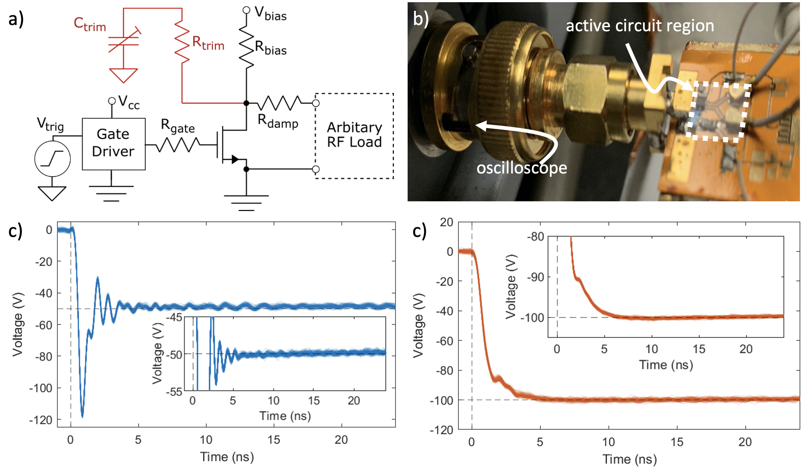
Figure 1b shows the realization of this circuit on a thick Kapton dielectric and copper substrate, directly coupled through an SMA and SMA-to-BNC adapter to the oscilloscope. The white shaded region shows the active area of the GaNFET, driver, bypass capacitors and damping, taking up less than , while the power supply makes up the rest of the circuit and can be placed off-board. Detailed optimization of the components and layout to minimize parasitic quantities and maximize switching speed is discussed in the supplement.
The undamped and damped response of the circuit coupled through a 2.2 pF capacitor to a 2 GHz LeCroy 6200A oscilloscope is shown in Figure 1c and d respectively. Initially we took measurements with a passive, 500 MHz, probe (LeCroy PP007-WR), but we found that the distributed nature of the probe complicated our attempts to reduce the circuit to a simple lumped element model. This is discussed further in the supplement. The undamped response at = 0 shows a full, 0% to 100% transition in 540 ps, but suffers from massive overshoot and significant ringing. To ensure we did not damage the oscilloscope with this overshoot, we kept this measurement to 50 V, though when measured by the probe we easily pushed this to 100 V as seen in Figure S4b in the supplement. The damped response obtained at = 200 shows a transition from -10 V to -90 V (10% to 90% of the amplitude) in less than 1.5 ns with no residual ringing, as shown in Figure 1c. More significantly, the damped circuit is capable of reaching 10% of the final voltage in under 1.9 ns, and 1% accuracy in 5.1 ns as shown in the inset of Figure 1d. We note that these circuits were successfully driven up to 200 volts without failure. However to ensure we did not damage the probe and oscilloscope, the maximum voltage at which we measured the transition was 100 V, as shown.
From these measurements, we can then estimated the parasitic quantities of our circuit. This assumes we can treat the whole system as lumped elements, which as discussed later is valid due to the small length scale of the GaNFET and load. Modeling the circuit as an series resistor, inductor, capacitor (RLC) circuit, as shown in Figure S5 in the supplement, we estimate the series capacitance to be 2 pF. This is calculated by putting the 20 pF oscilloscope capacitance in parallel with the 2.2 pF capacitor, and is validated by the 1:10 attenuated voltage transition we measure on the oscilloscope.
We then measure the ringing frequency of the undamped load. This is approximately 1.1 GHz. Assuming that this measurement is relatively undamped, we can then use Eqn. 1 below to estimate the loop inductance. Here is the oscilloscope inductance, the ringing frequency, and the oscilloscope capacitance see through the 2.2 pF coupling capacitor. This leads us to estimate the inductance to be 10 nH, which is roughly consistent with the damping we required to prevent ringing. This is also validated by the fact that commonly used RG-58/U coaxial cable has an inductance of 3.66 nH/cm, and the measured connector to oscilloscope length is 3 cm, meaning we would expect the cabling to give us 11 nH of inductance.
| (1) |
The response times of both of these transitions are limited by the inductance of the oscilloscope path, which results in a 1.1 GHz resonance. If we wanted an even faster measurement, we could try to reduce the loop inductance of the measurement by putting the GaNFET even closer to the oscilloscope. We could also use active probing, though these probes generally have voltage ratings too low for such high power switches and still perturb the circuit greater than many loads we are interested in. Furthermore, we are most interested in the fields generated in the loads of interest, not the voltage at different conductors, which probing can never directly tell us. Thus, we used RF simulations to estimate the more fundamental field switching capabilities of these circuits important to many real-world applications.
III Simulation of Response to Realistic Loads
In order to validate the performance of the GaNFET pulser for switching realistic loads, we simulated the GaNFET pulser’s switching performance in various systems, including a primarily capacitive load, a primarily inductive load, and a load with characteristics of both, as shown in Figure 2a, Figure 3d, and Figure 3a respectively.
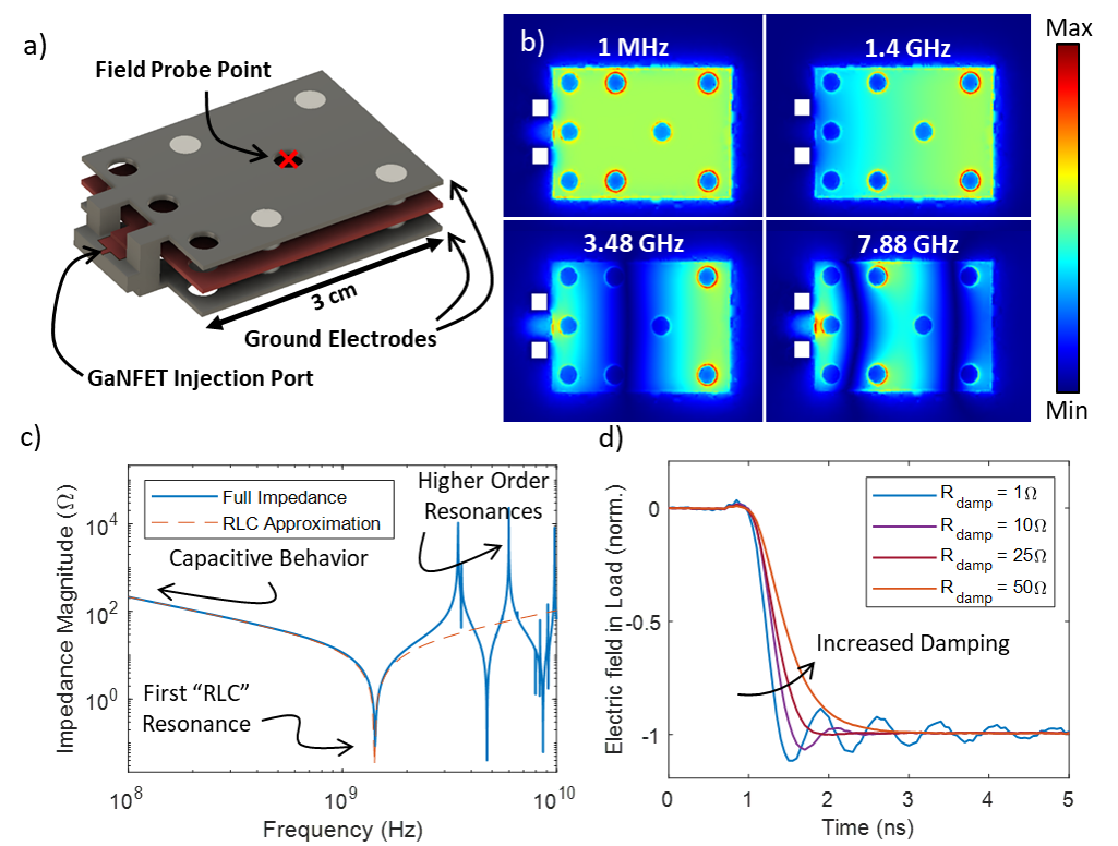
The basic approach and results of these simulations are outlined in Figure 2a-d. First, we defined a geometric structure in COMSOL Multiphysics to be excited. In the case of the primarily capacitive load, we defined three 304 stainless steel plates from Kimball Physics stacked with alumina spacers, with the central electrode (red) receiving the GaNFET excitation as shown in Figure 2a. This kind of structure is widely used in electron optics for the fast gating (if the beam enters vertically) and deflection (if the beam enters horizontally) of charged particles. We defined the source and drain of the GaNFET to be our input ports for the simulations.
Using the RF Module in COMSOL, we ran a full wave simulation of the structure in the frequency domain, extracting both the field distributions in the load and the port impedance seen by the GaNFET, as shown in Figure 2b and 2c respectively. The rational fit and the circuit model of the port impedance was generated in MATLAB and imported into LTSpice to simulate the voltage at the port. This is shown in the supplement. Then in MATLAB, we took the Fourier transform of this output voltage and multiplied it with the voltage-to-field transfer function at the point indicated by the red x in Figure 2a to get the frequency response of the field in the load. Finally, we took the inverse Fourier transform of the field response, resulting in the time-domain plot shown in Figure 2d. This process is shown in Figure S8 of the supplement. Here, in Figure 2d, we can see a steady decrease of the load ringing as we increase the damping resistance from to . At a damping of we see the fastest ringing-free transition, which corresponds to a 200 V transition in less than 1 ns. The underlying switching performance and its dependence on is consistent with the measurement on a similarly resonant load, the oscilloscope-GaNFET system resonant at 1.1 GHz, as shown by the ringing in Figure 1d.
We next worked to simplify the treatment of this load and remove ringing of the field at the point of interest. Generally, it is assumed that the wavelength of the exciting voltage is significantly larger than the length scale of the load, we can treat that system as a lumped circuit with parasitic quantities C and L associated with it Pozar (2009). Explicitly, we require
| (2) |
where is the wavelength, the propagation velocity in the medium (in this case just for vacuum), and the frequency of interest. This approximation is generally held valid if the structure length-scale is .
We can see this lumped element behavior emerge explicitly in the impedance plotted in Figure 2c. At frequencies below 500 MHz, the parallel plates exhibit the characteristic of a 7.38 pF capacitor. As the frequency increases beyond 500 MHz and approaches the first resonance at 1.4 GHz, the load is no longer purely capacitive, but is well-modeled using an RLC resonant circuit with an inductance of 1.70 nH as shown in the Figure 2c. However, above 2 GHz, the system can no longer be treated as an 2nd-order LC lumped circuit due to the many resonant modes developed by the length scale of the load, some examples of which are shown in Figure 2b.
This simplified RLC lumped element treatment offers significant advantage in the ability to estimate and remove ringing in our system. By treating the load as a lumped RLC model, it becomes significantly easier to understand the effects of the parasitic output capacitance and inductance of the driving FET. This treatment also allows “critical dampening” of the circuit with an appropriately selected series resistance, dramatically simplifying the filter design that would normally be needed for such a precise transition. This is demonstrated in Figure 2d, where a damping resistance is selected to cause a highly smooth transition that resembles a critical damping in RLC circuits. Ringing-like behavior at 4 GHz and above still does exist in the output, though it is significantly attenuated to below 1% the transition magnitude.
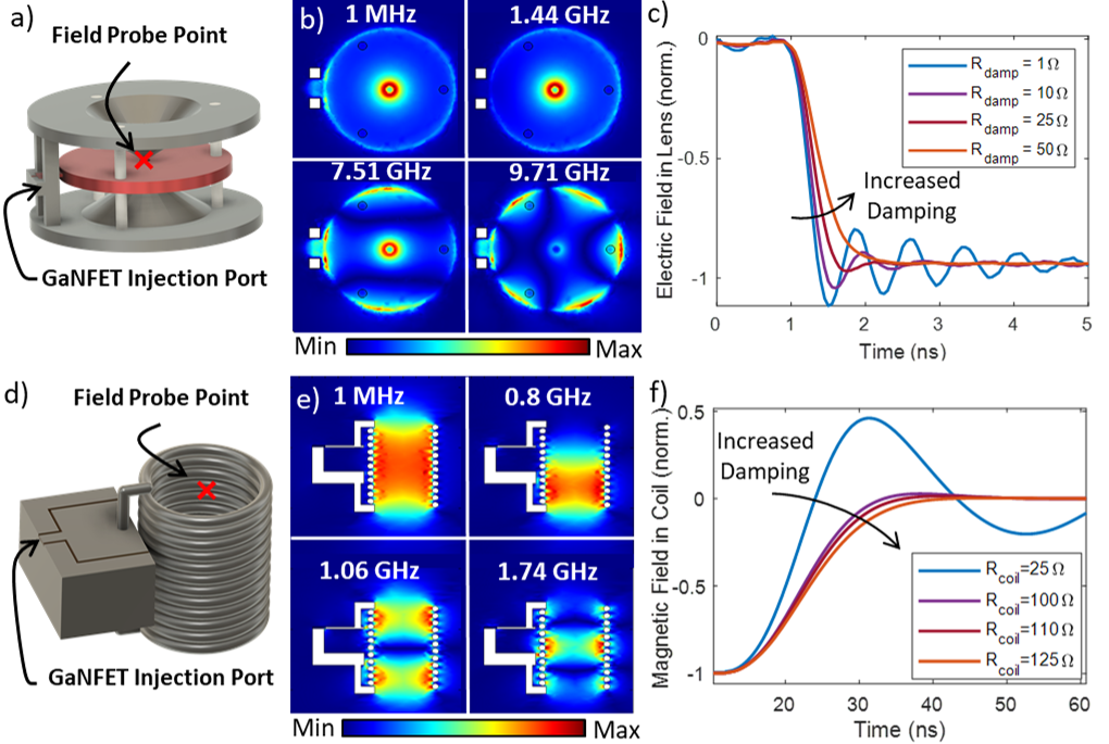
We also examined other loads to validate the generality of this approach. In Figure 3a-c we show driving of a high voltage Einzel lens. This kind of structure is used commonly in electron optics, where the varied spacing of plates is designed to allow for high-strength fields near the center, while the wider spaced portion near the edges prevent electrical breakdown at the insulators during high voltage operation 201 (2017). This load has varied capacitance from the outside of the structure to the inside, as well as a much more significant inductive component due to the large ground return loop. Various resonances of this structure are shown in Figure 3b, and we can clearly see stronger electric fields near the center due to the closer plate spacing. Unlike the first capacitor model, this load cannot be easily simplified into a transmission line segment and thus matched to systems. However, the load can still be simplified into 5.50 pF capacitive model at low frequencies and a series RLC circuit with 2.35 nH inductance at higher frequencies. This fit is shown in Figure S9a of the supplement. This higher inductance and lower capacitance is consistent with the larger ground return path of this structure compared to the primarily capacitive load. As before, using GaNFET driving and dampening of the first RLC resonance, it was possible to generate a ringing-free field transitions in the load at the field probe point, this time in 1.2 ns, slightly slower. The generated field strength is equivalent to that that would be generated from a 200 V potential applied to the center electrode. It is interesting to note that nominally the first resonance of this lens and the first deflector are roughly the same, but this lens has a slightly slower response. This is due to the output capacitance of the GaNFET in the LTSpice model, which results in a response that is much more sensitive to the inductance of the load. This is discussed in the supplement in greater detail.
Another load we drove is the inductive coil shown in Figure 3a, which primarily generates a magnetic field rather than an electric field and is used commonly for applying strong magnetic fields to samples and for electron beam deflection systems 201 (2017). The driving topology for this circuit is different from that of the previous cases due to the low DC impedance of the load. This is shown in the supplement. At low frequencies, this element behaves as a near perfect 313 nH inductor, with an impedance that increases linearly as a function of frequency. As the frequency increases, the capacitance between the wires begin to shunt current, resulting in a reduced impedance and more concentrated fields near the edges as shown in Figure 3e. When the first resonance is reached around 260 MHz, we can model the circuit as a parallel RLC circuit with a capacitance of 1.15 pF. Similar to the previously discussed loads, we were able to tune to achieve a ringing-free magnetic field response driven by a current as shown in Figure 3f. However, due to the large inductive component coupled to the GaNFET’s output capacitance, this load requires a larger resistance of 110 to damp, slowing the response substantially. Although the current transition time of roughly can be shortened by reducing the loop size or number, inductive loads will almost always be slower that capacitive loads due to the fixed output capacitance of the GaNFET circuit and layout.
IV Discussion
Besides providing fast, ringing-free switching of hundreds of volts and tens of amperes, the GaNFET switches described above also offer the following useful features. (1) Affordability. The circuit shown in Figure 1b is simple to assemble using standard soldering tools, and costs two-orders-of magnitude less than commercial pulsers. This enables wide use in a range of experimental apparatus. (2) Compatibility with computer and FPGA driving. These circuits also offer simple and arbitrary control by 3.3 V pulses on lines; (3) repetition rates up to 60 MHz (if a high side P-Channel transistor is used rather than the resistor), in comparison to several KHz for spark gap technologies Rahaman et al. (2010) and 25 MHz for custom state-of-the-art avalanche circuits Beev, Keller, and Mehlstäubler (2017); (4) 2.5 ns propagation delays which open the possibility of real-time control based on triggering of other single-shot measurements in an apparatus; (5) a < active form factor that allows for the integration of these circuits extremely close to the loads they drive, minimizing parasitic energy storage that slow transitions; (6) <1 W power dissipation at 10 MHz, which scales approximately linearly with the circuit repetition rate. The low power dissipation means that it is possible to operate these circuits under vacuum, a requirement for driving loads such as charged particle optics in this manner.
The pulsers discussed so far have been optimized for single-sided driving, where one transition (the negative sloped one) is on the order of nanoseconds, while the reset transition is on the order of tens of nanoseconds. This maximizes the speed of the faster edge and simplifies the circuit design significantly, though limits the technique in terms of repetition rates and for some applications. In order to drive both positive and negative edges, alternative topologies such as a half-bridge configuration with bootstrapping is required. Commercial drivers, such as the LMG1210 from Texas Instruments, do exist for this, though the increased size and complexity of the circuitry slows their transition times. Also note that fully integrated GaNFET circuits do exist, such as the LMG3410 from Texas Instruments, though have slower switching transitions than demonstrated here.
By varying the FET technology and topology, this approach can be extended to switching even higher voltages and currents. The simplest way of doing this is to vary the GaNFET technology, using for example the GS61004B from GaN Systems or the TP65H070LSG from Transphorm, both of which are capable of 650 V operation, though their increased gate capacitance, output capacitance, and parasitic inductance lead to slowed output transitions. Another approach would be to use SiC technology, allowing for transitions of several thousand volts though at the cost of even slower transitions. Alternate topologies used historically to improve silicon performance, such as parallel and stacked FETs Jiang (2007) or cascode configurations Baker and Johnson (1992) could also be used to improve both voltage ratings and transition performance in these GaN systems.
Several routes also could be used to increase the speed of these switches to achieve subnanosecond transitions. Smaller, lower voltage FETs such as the 100 V EPC2037 from the Efficient Power Corporation would have significantly faster switching due to its smaller gate and output capacitance, as well as its lower form factor. For low voltages and medium currents of 5 A, GaNFET gate drivers such as the LMG1020 itself could also be used directly to drive loads with 400 ps transition times. If state-of-the-art rise times are desired, non-linear pulse sharpening techniques such as step recovery diodes Wong Choi, Joo Choi, and Hoon Han (2011) and nanoplasmas Samizadeh Nikoo et al. (2020) could be used together with these FETs, which would allow for transitions on the order 100 ps or less, and would not increase layout size significantly.
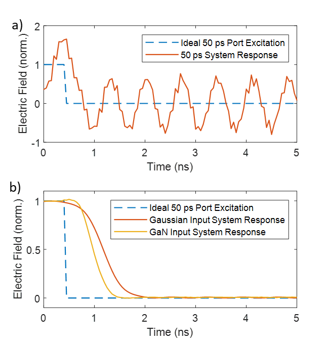
A natural question that arises as we increase the speed of the transitions is how fast the loads fundamentally can be driven, especially when trying to ensure no ringing. Even if we drove the load with an ideal 100 ps step, the high-frequency resonances of the load would drown out the signal in ringing and drag out the transition. This is demonstrated in Figure 4a for the real load in Figure 2a. If we then put this transition through an ideal Gaussian filter to reduce the pulse bandwidth and reduce the ringing to 1% the transition, we get the result in Figure 4b which is significantly slower, taking roughly 2 ns to get within 1% accuracy. This transition is significantly slower than the RLC response also shown in Figure 4b, which took only 1.2 ns to achieve equivalent accuracy. Different filtering schemes, such as Chebyshev or Butterworth filters might improve this further, but these were not explored.
Two general approaches come to mind for driving these loads faster: optimizing the load structure to minimize resonances, and shaping the incident signal to avoid these resonances. The first relies on pushing the load resonances up or reducing their magnitude. Increasing the resonances can be achieved by reducing the physical size of the load and avoiding the use high permeability and permittivity materials. Reducing their quality factor can be done by introducing surface roughness to the load, increasing the structures resistivity with different materials or coatings, or introducing a lossy propagating media. However, we have not explored any of these routes in depth.
The input engineering approach can be realized with various schemes of increasing complexity. The simplest approach would be to use a low-pass filter to generate a transition with a sharper cutoff that excites the first resonance less than the Gaussian filter we simulated. Exactly how much faster you could drive this circuit with that is unclear and depends strongly on the load and specific filter used. A second approach that would give a faster response would be to design a resonant filter that selectively removes the strongest resonant peaks in the output. Exactly how accurately one could find and remove these resonances and to what bandwidth is unclear. A third approach similar to the resonant one would be to use an arbitrary waveform generator (AWG) to digitally generate create an input signal with the resonant modes removed. This would remove ringing to the bandwidth and gain to the limits of the AWG and amplifier used, though again probing to precisely remove the ringing would be a challenge. This approach has been explored in recent work Klopfer et al. (2020).
V Conclusion
In this work, we demonstrated the potential of inexpensive GaN power electronics to switch real loads commonly found in physics and engineering with high power and few-nanosecond, ringing-free transitions. We first validated this concept by constructing a test-bed circuit capable of switching in 250 ps with ringing, and 1.5 ns without ringing. This was done with a design using raw parts costing two orders of magnitude less than comparable commercial pulse generators. Switching up to 200 V was tested to ensure the switch did not fail, but was never measured in operation due to concerns of damaging the oscilloscope used. Due to our inability to reduce measurement parasitics at such high voltages, and in order to see the field distribution with a real load, we simulated the output of the circuit for various structures ranging from capacitive to inductive. We then extracted the temporal response of the electric and magnetic fields in the load at various points, demonstrating 1 ns, ringing-free switching for the provided capacitive loads. We also demonstrated a model of each load’s lowest resonance as an RLC resonator, which allowed us to simplify analysis of the load and damp the dominant ringing of the field. We demonstrated that although higher frequency components theoretically remained, they were negligible and the switching behaved much like a critically-damped circuit.
We noted that this pulser is theoretically capable of being controlled directly and arbitrarily by 5 V logic signals up to 60 MHz, with 2.5 ns propagation delays, limited in the current iteration by circuit resetting from the biasing resistance. We also discussed the the possibility of integrating this circuit in environments such as vacuum as well as using other pulsing topologies to increase the current and voltage ratings even further. We finally discussed the limits of real load switching and demonstrated this work provides a faster response than ideal Gaussian low-pass filtering can provide. Future work will expand upon these results by integrating these circuits under vacuum with deflectors and measuring the time dependence of GaN-switched loads directly using electron beams, the smallest probe imaginable. We believe this work will have significant application throughout physics where inexpensive, simple, high voltage, and precise switching is needed.
Acknowledgements.
This work was supported by the Gordon and Betty Moore Foundation. This material is based upon work supported by the National Science Foundation Graduate Research Fellowship under Grant No. 1745302. Yugu Yang-Keathley and Ben Slayton acknowledge support from the Douglas D. Schumann Professorship. The authors thank Marco Turchetti and Navid Abedzadeh for help with designing the original structures simulated, Texas Instruments for providing internal SPICE models of the LMG1020 used in the simulations, and the QEM-II collaboration for insightful discussions. In particular, we would like to thank the Kasevich group at Stanford, especially Adam Bowman, Brannon Klopfer, and Stewart Koppell, for many discussions of fast pulsing technology, alternative techniques to drive such loads, and applications of these pulsers. The authors also thank Ilya Charaev and Owen Medeiros for helpful feedback on the manuscript.References
- Bishop and Barker (2006) A. I. Bishop and P. F. Barker, “Subnanosecond Pockels cell switching using avalanche transistors,” Review of Scientific Instruments 77, 1–6 (2006).
- Wolff and Stephens (1953) M. M. Wolff and W. E. Stephens, “A pulsed mass spectrometer with time dispersion,” Review of Scientific Instruments 24, 616–617 (1953).
- Zhang et al. (2020) L. Zhang, M. W. Garming, J. P. Hoogenboom, and P. Kruit, “Beam displacement and blur caused by fast electron beam deflection,” Ultramicroscopy 211, 112925 (2020).
- Zajfman et al. (1997) D. Zajfman, O. Heber, L. Vejby-Christensen, I. Ben-Itzhak, M. Rappaport, R. Fishman, and M. Dahan, “Electrostatic bottle for long-time storage of fast ion beams,” Physical Review A 55, R1577–R1580 (1997).
- Kruit et al. (2016) P. Kruit, R. G. Hobbs, C. S. Kim, Y. Yang, V. R. Manfrinato, J. Hammer, S. Thomas, P. Weber, B. Klopfer, C. Kohstall, T. Juffmann, M. A. Kasevich, P. Hommelhoff, and K. K. Berggren, “Designs for a quantum electron microscope,” Ultramicroscopy 164, 31–45 (2016).
- Jiang (2007) W. Jiang, “Fast high voltage switching using stacked MOSFETs,” IEEE Transactions on Dielectrics and Electrical Insulation 14, 947–950 (2007).
- Chaney and Sundararajan (2004) A. Chaney and R. Sundararajan, “Simple MOSFET-based high-voltage nanosecond pulse circuit,” IEEE Transactions on Plasma Science 32, 1919–1924 (2004).
- Baker and Johnson (1992) R. J. Baker and B. P. Johnson, “A 500 V nanosecond pulse generator using cascode-connected power MOSFETs,” Measurement Science and Technology 3, 775–777 (1992).
- Jinyuan, Bing, and Zenghu (1998) L. Jinyuan, S. Bing, and C. Zenghu, “High voltage fast ramp pulse generation using avalanche transistor,” Review of Scientific Instruments 69, 3066–3067 (1998).
- Henebry (1961) W. M. Henebry, “Avalanche transistor circuits,” Review of Scientific Instruments 32, 1198–1203 (1961).
- Benzel and Pocha (1985) D. M. Benzel and M. D. Pocha, “1000-V, 300-ps pulse-generation circuit using silicon avalanche devices,” Review of Scientific Instruments 56, 1456–1458 (1985).
- Zou, Gupta, and Caloz (2017) L. Zou, S. Gupta, and C. Caloz, “A simple picosecond pulse generator based on a pair of step recovery diodes,” IEEE Microwave and Wireless Components Letters 27, 467–469 (2017).
- Afshari and Hajimiri (2005) E. Afshari and A. Hajimiri, “Nonlinear transmission lines for pulse shaping in silicon,” IEEE Journal of Solid-State Circuits 40, 744–752 (2005).
- (14) Carl E. Baum, L. Carin, and A. P. Stone, Ultra-Wideband, Short-Pulse Electromagnetics.
- Mourou and Knox (1979) G. Mourou and W. Knox, “High-power switching with picosecond precision,” Applied Physics Letters 35, 492–494 (1979).
- Kohler et al. (2013) S. Kohler, V. Couderc, R. O’Connor, D. Arnaud-Cormos, and P. Leveque, “A versatile high voltage nano-and sub-nanosecond pulse generator,” IEEE Transactions on Dielectrics and Electrical Insulation 20, 1201–1207 (2013).
- De Angelis et al. (2011) A. De Angelis, M. Dionigi, R. Giglietti, and P. Carbone, “Experimental comparison of low-cost sub-nanosecond pulse generators,” IEEE Transactions on Instrumentation and Measurement 60, 310–318 (2011).
- Martin (1992) J. C. Martin, “Nanosecond Pulse Techniques,” Proceedings of the IEEE 80, 934–945 (1992).
- Mankowski and Kristiansen (2000) J. Mankowski and M. Kristiansen, “A review of short pulse generator technology,” IEEE Transactions on Plasma Science 28, 102–108 (2000).
- Samizadeh Nikoo et al. (2020) M. Samizadeh Nikoo, A. Jafari, N. Perera, M. Zhu, G. Santoruvo, and E. Matioli, “Nanoplasma-enabled picosecond switches for ultrafast electronics,” Nature 579, 534–539 (2020).
- Klopfer et al. (2020) B. B. Klopfer, S. A. Koppell, A. J. Bowman, Y. Israel, and M. A. Kasevich, “RF pulse shaping for gated electron mirrors,” , 1–5 (2020).
- Wu et al. (2008) Y. Wu, M. Jacob-Mitos, M. L. Moore, and S. Heikman, “A 97.8% efficient GaN HEMT boost converter with 300-W output power at 1 MHz,” IEEE Electron Device Letters 29, 824–826 (2008).
- Brown et al. (2011) A. Brown, K. Brown, J. Chen, K. C. Hwang, N. Kolias, and R. Scott, “W-band GaN power amplifier MMICs,” IEEE MTT-S International Microwave Symposium Digest , 11–14 (2011).
- Glaser (2018) J. S. Glaser, “High power nanosecond pulse laser driver using a gan fet,” PCIM Europe Conference Proceedings , 662–669 (2018).
- Amano et al. (2018) H. Amano, Y. Baines, E. Beam, M. Borga, T. Bouchet, P. R. Chalker, M. Charles, K. J. Chen, N. Chowdhury, R. Chu, C. D. Santi, M. M. D. Souza, S. Decoutere, L. D. Cioccio, B. Eckardt, T. Egawa, P. Fay, J. J. Freedsman, L. Guido, O. Häberlen, G. Haynes, T. Heckel, D. Hemakumara, P. Houston, J. Hu, M. Hua, Q. Huang, A. Huang, S. Jiang, H. Kawai, D. Kinzer, M. Kuball, A. Kumar, K. B. Lee, X. Li, D. Marcon, M. März, R. McCarthy, G. Meneghesso, M. Meneghini, E. Morvan, A. Nakajima, E. M. S. Narayanan, S. Oliver, T. Palacios, D. Piedra, M. Plissonnier, R. Reddy, M. Sun, I. Thayne, A. Torres, N. Trivellin, V. Unni, M. J. Uren, M. V. Hove, D. J. Wallis, J. Wang, J. Xie, S. Yagi, S. Yang, C. Youtsey, R. Yu, E. Zanoni, S. Zeltner, and Y. Zhang, “The 2018 {GaN} power electronics roadmap,” Journal of Physics D: Applied Physics 51, 163001 (2018).
- Lidow et al. (2019) A. Lidow, M. de Rooij, J. Strydom, D. Reusch, and J. Glaser, GaN Transistors for Efficient Power Conversion (2019).
- Instruments (2018) T. Instruments, “LMG1020 data sheet,” Tech. Rep. (2018).
- Pozar (2009) D. M. Pozar, Microwave Engineering (Wiley, New York, 2009).
- 201 (2017) Handbook of Charged Particle Optics (2017).
- Rahaman et al. (2010) H. Rahaman, J. W. Nam, S. H. Nam, and K. Frank, “A miniaturized spark gap switch in the regime of high repetition rate,” Proceedings of the 2010 IEEE International Power Modulator and High Voltage Conference, IPMHVC 2010 , 385–387 (2010).
- Beev, Keller, and Mehlstäubler (2017) N. Beev, J. Keller, and T. E. Mehlstäubler, “Note: An avalanche transistor-based nanosecond pulse generator with 25 MHz repetition rate,” Review of Scientific Instruments 88 (2017), 10.1063/1.5000417.
- Wong Choi, Joo Choi, and Hoon Han (2011) G. Wong Choi, J. Joo Choi, and S. Hoon Han, “Note: Picosecond impulse generator driven by cascaded step recovery diode pulse shaping circuit,” Review of Scientific Instruments 82 (2011), 10.1063/1.3523342.