First principles design of Ohmic spin diodes based on quaternary Heusler compounds
Abstract
The Ohmic spin diode (OSD) is a recent concept in spintronics, which is based on half-metallic magnets (HMMs) and spin-gapless semiconductors (SGSs). Quaternary Heusler compounds offer a unique platform to realize the OSD for room temperature applications as these materials possess very high Curie temperatures as well as half-metallic and spin-gapless semiconducting behavior within the same family. Using state-of-the-art first-principles calculations combined with the non-equilibrium Green’s function method we design four different OSDs based on half-metallic and spin-gapless semiconducting quaternary Heusler compounds. All four OSDs exhibit linear current-voltage () characteristics with zero threshold voltage . We show that these OSDs possess a small leakage current, which stems from the overlap of the conduction and valence band edges of opposite spin channels around the Fermi level in the SGS electrodes. The obtained on/off current ratios vary between and . Our results can pave the way for the experimental fabrication of the OSDs within the family of ordered quaternary Heusler compounds.
Spintronics is a rapidly emerging field in current nanoelectronics. Due to their diverse and tunable electronic and magnetic properties, Heusler compounds received great interest for potential applications in spintronics. Especially, within the last two decades half metallic Heusler compounds with 100% spin polarization of the conduction electrons at the Fermi energy [1] have been extensively studied; both, theoretically and experimentally, for memory and sensor applications. Besides half metallicity in ordinary X2YZ-type Heusler compounds, several quaternary Heuslers with chemical formula XX’YZ, with , and are transition-metal atoms and is an element, have been theoretically predicted to exhibit spin-gapless semiconducting behavior and some of them have been experimentally synthesized [2, 3, 4, 5]. Spin-gapless semiconductors (SGSs) possess a unique electronic structure, in which conduction- and valence-band edges of opposite spins touch at the Fermi level [6] and thus SGS behavior leads to unique functionalities and device concepts.
| mX | m | mY | m | MAE111Out-of-plane magnetisation is marked as negative MAE | Ground | |||||||
|---|---|---|---|---|---|---|---|---|---|---|---|---|
| HMM-SGS junction | Coupling | Compound | (Å) | () | () | () | () | (eV) | (eV/at.) | (K) | state | |
| MnVTiAlFeVTaAl | FeVTaAl | 6.10 | 1.00 | 0.85 | 2.38 | -0.19 | 3.00 | 3.75 | 0.63 | 681 | SGS | |
| MnVTiAl | 6.10 | 1.01 | -2.42 | 2.61 | 0.86 | 1.00 | 3.59 | 11.94 | 963 | HMM | ||
| FeVHfAlFeVTiSi | FeVTiSi | 5.91 | 1.00 | 0.57 | 2.33 | 0.10 | 3.00 | 3.52 | -0.94 | 464 | SGS | |
| FeVHfAl | 5.91 | 1.12 | -0.15 | 2.06 | 0.10 | 2.00 | 4.10 | 117.44 | 742 | HMM | ||
| FeVHfAlFeVNbAl | FeVNbAl | 6.11 | 1.00 | 0.81 | 2.32 | -0.11 | 3.00 | 3.72 | 0.25 | 693 | SGS | |
| FeVHfAl | 6.11 | 1.04 | -0.68 | 2.41 | 0.29 | 2.00 | 3.45 | 62.44 | 742 | HMM | ||
| Co2MnSiFeVTaAl | FeVTaAl | 6.10 | 1.00 | 0.79 | 2.32 | -0.11 | 3.00 | 3.75 | 0.63 | 681 | SGS | |
| CoCoMnSi | 6.10 | 0.86 | 1.01 | 1.01 | 3.18 | 5.00 | 3.83 | 57.50 | 920 | HMM |
Half-metallic Heusler compounds have been considered as ideal electrode materials in magnetic tunnel junctions for spin-transfer torque magnetic memory applications due to their very high Curie temperatures. The use of Co-based Heusler compounds in magnetic tunnel junctions made the experimental observation of high tunnel magnetoresistance (TMR) effects possible. [8, 9, 10, 11, 12] However, magnetic tunnel junctions constructed with half metals do not present any rectification (or diode effect) for logic operations. Lately logic functionality in magnetic tunnel junctions is achieved by replacing one of the electrodes by a SGS material. In Ref. 13, based on HMMs and SGSs, a reconfigurable magnetic tunnel diode and transistor has been proposed. This concept combines logic and memory on the diode and transistor level. Moreover, in a recent publication the present authors proposed another device concept based on HMMs and SGSs, which is the so-called Ohmic spin diode (OSD) [14]. It has been computationally demonstrated that the OSD comprising two-dimensional half-metallic Fe/MoS2 and spin-gapless semiconducting VS2 exhibits linear current-voltage () characteristics with zero threshold voltage . OSDs have a much higher current drive capability and low resistance, which is advantageous compared to conventional semiconductor junction diodes and metal-semiconductor Schottky diodes.
The aim of the present Letter is a computational design of OSDs based on quaternary Heusler compounds for room temperature applications. Heusler compounds offer a unique platform to realize the OSD as these materials possess very high Curie temperatures (much above room temperature) as well as half-metallic and spin-gapless semiconducting behavior within the same family. To this end, the selection of the SGS and HMM electrode materials from the Heusler family for the design of OSDs is based on our recent study in Ref. 7, where we focus on Curie temperatures, spin-gaps, formation energy, Hull distance for a large number of quaternary Heusler compounds. Among the considered materials three SGSs (FeVNbAl, FeVTaAl, and FeVTiSi) turn out to be promising for device applications. As for the half-metallic Heusler compounds, we have a large variety of choice, but we stick to the quaternary ones (MnVTiAl, FeVHfAl) with similar lattice constants to the SGSs in order to ensure a coherent growth on top of each other. Additionally, we also consider the well-known half-metallic Co2MnSi system among the ordinary full Heusler compounds as an electrode material.
Our first-principles design of the OSDs is based on the density functional theory (DFT) using the QuantumATK package (version P-2019.12) [15, 16]. As exchange-correlation functional we chose the Perdew-Burke-Ernzerhof (PBE) parametrization [17] combined with norm-conserving PseudoDojo pseudopotentials [18] and linear combinations of atomic orbitals (LCAO) as basis-set. As -point grid for the ground state properties we use a Monkhorst-Pack grid and a density mesh cutoff of 120 Hartree. For the transport calculations we combined DFT with the nonequilibrium Green’s function method (NEGF). We use a -point mesh in self-consistent DFT-NEGF calculations. The characteristics were calculated within the Landauer approach [19], where . stands for the bias voltage and the transmission coefficient depends additionally on spin of an electron and energy . Furthermore, and denote the Fermi-Dirac distribution of the left and right electrode, respectively. For the calculation of we chose a -point grid.
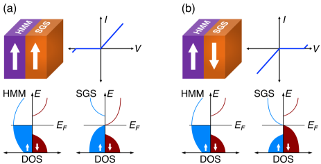
In Fig. 1 we present schematically the structure of the OSD and the corresponding characteristics. The concept of the OSD has been extensively discussed in Ref. 14 and thus here we will only give a short overview of the device. The OSD consists of HMM and SGS materials and possesses linear characteristics. The schematic DOS of these materials are also shown in Fig. 1. Depending on the choice of the junction materials, the HMM and SGS electrodes can couple ferromagnetically (ferromagnetic OSD) or antiferromagnetically (antiferromagnetic OSD) at the interface giving rise to corresponding curves shown in Fig. 1. The operation principle of the OSD relies on the unique spin-dependent transport properties of HMMs and SGSs as discussed in Ref. 14 in detail.
In the proposal of the OSD [14], the proof of principle was demonstrated by using two dimensional transition-metal dichalcogenides VS2 (SGS) and Fe/MoS2 (HMM) as electrode materials. Since VS2 possesses an estimated Curie temperature of 138 K [20], it is not suitable for room temperature applications. For more realistic devices we now consider six Heusler compounds as mentioned before and construct four different OSDs: i) FeVHfAl FeVTiSi, ii) FeVHfAlFeVNbAl, iii) MnVTiAlFeVTaAl, and iv) Co2MnSiFeVTaAl. All six Heusler compounds possess extremely high Curie temperatures as presented in Table 1. For the construction of the OSD we assume the situation where one material needs to be grown on top of the other one. Thus, in our simulations we take one electrode (SGS) in the cubic structure and relax the second electrode material (HMM) with respect to the in-plane lattice parameter of the first one. Therefore, in Table 1 we include the ratios for the half metallic electrode materials which takes the tetragonal structure. In Table 1 we present also the obtained magnetic moments, magnetic anisotropy energies (MAEs), and work functions. As expected, tetragonal distortion results in a significant change in the magnetic anisotropy energy of HMMs, which is at least two orders of magnitude larger than the SGSs, being in good agreement with the literature [21].
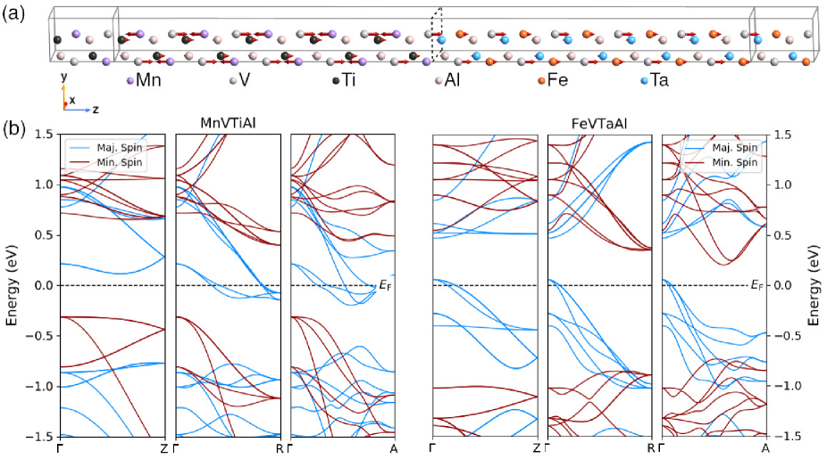
We now focus on the first OSD and discuss its structural, electronic and magnetic properties. Fig. 2 (a) illustrates the atomic structure of the OSD based on half-metallic MnVTiAl (left electrode) and spin-gapless semiconducting FeVTaAl (right electrode) quaternary Heusler compounds. We use a minimal tetragonal unit cell along the [001] direction containing 8 atoms. For each electrode this cells was repeated 5 times and defines the screening region. The length (screening region) of the device is around 62 Å. In the other three OSDs, the considered screening region lies in between 61Å and 63Å, depending on the materials. As the strength of the spin-orbit coupling (SOC) is very weak in these materials we, neglect the SOC in transport calculations and thus we chose the -direction as the transport direction and also adjusted the alignment of the magnetic moments to the -axis. The red arrows and their size in Fig. 2 (a) represent the direction and magnitude of the atomic magnetic moments in the junction materials. In this OSD, the HMM and SGS electrodes couple ferromagnetically at the interface, i.e., the energy difference between ferromagnetic and antiferromagnetic coupling is about 400 meV.
Looking at the magnetic moments at the interface region in Fig. 2, we notice that the size of the arrows deviate from their bulk behavior, i.e, far from the interface. Especially the magnetic moment of the Mn atom in MnVTiAl at the interface decreases from 2.42 to 0.07 . This is due to the fact, that at the interface region MnVTaAl is formed which also presents HMM behavior with bulk magnetic moments of , , and . Therefore, the half metallic character of the MnVTiAl compound is retained at the interface. However, the FeVTaAl compound loses its spin-gapless semiconducting nature near the interface region as it will be discussed later in detail.
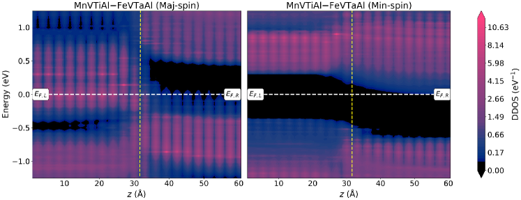
Next, we would like to discuss the electronic properties of the MnVTiAlFeVTaAl junction at equilibrium, i.e., at zero bias. The bulk band structure along the transport direction of the junction materials is shown in Fig. 2 (b). MnVTiAl is a HMM with a band gap of around 650 meV in the minority-spin channel while FeVTaAl shows SGS properties. Note that the spin-gapless semiconducting behavior along the chosen directions is not well seen and for a detailed discussion the reader is referred to Refs. 4 and 7. Nikolaev et al. [22] and Bai et al. [23] provided a detailed discussion about the importance of band matching for the transport properties of giant magnetoresistance (GMR) spintronic devices. In our case, as seen in Fig. 2 (b), there is a good band matching for the majority spin states near the Fermi level close to the -point between the electrode materials, especially along the -R and -A directions. Note that a good band matching suppresses the electron back scattering at the interface and ensures a smooth propagation of majority spin electrons from the FeVTaAl electrode to the MnVTiAl electrode. In Fig. 3 we present the device density of states (DDOS) of the MnVTiAlFeVTaAl junction. As mentioned above the half metallicity of MnVTiAl is preserved at the interface which can be seen in the majority-spin and minority-spin channel DDOS presented in Fig. 3. However, the SGS character of FeVTaAl is lost near the interface region due to the charge transfer from the half-metallic electrode to the SGS (see the left panel of Fig. 3). This charge transfer stems from the work function difference of 160 meV between the two electrode materials. As MnVTiAl has the lower work function, electrons flow from the majority-spin channel of MnVTiAl to the majority spin-channel of FeVTaAl. Once the charge redistribution reaches equilibrium, MnVTiAl will be positively charged near the interface region, whereas FeVTaAl will be negatively charged and hence an electric dipole will be induced. This dipole influences the electronic and magnetic properties of both materials. Since the magnetic moment of the Mn atom in the MnVTiAl electrode has already been discussed above, we will briefly comment on the magnetic moment of the V atoms near the interface region.The magnetic moment of the V atoms in MnVTiAl is reduced to 2.25 close to the interface and recovers to the bulk value within two unit cells. On the other hand, the variation of magnetic moments in the FeVTaAl electrode near the interface region is around 0.1. Thus, the affected region by the charge transfer is restricted to five atomic layers for the majority-spin channel. The minority-spin channel is not substantially affected for both junction materials.
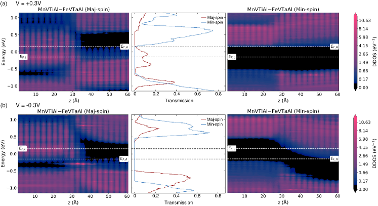
Up to now, we discussed the properties of the OSD for zero bias and will now focus on the current-voltage () characteristics when a bias voltage is applied. Therefore, Fig. 4 (a) and 4 (b) illustrate the DDOS for both spin channels for the MnVTiAlFeVTaAl junction under a bias voltage of +0.3 V and -0.3 V, respectively. Also the corresponding transmission spectra are presented there. For both, forward and reverse bias, the electronic and magnetic properties of both materials are not influenced by the bias voltage. The characteristics of the MnVTiAlFeVHfAl junction presented in Fig. 5 (a) can be explained on the basis of the DDOS. Under a forward bias voltage majority spin electrons from the occupied states below the Fermi level in FeVTaAl can be transmitted to unoccupied states above the Fermi level in MnVTiAl. Thus, the transmission coefficient has a finite value in this case. However, for the minority spin electrons the transmission coefficient is zero because both materials have no states that could contribute to transport in the given voltage window. Thus, the forward current (on-current) is 100% spin polarized. Also under an applied reverse bias voltage the transmission coefficient for minority-spin electrons is zero due to the energy gap in both materials. On the other hand, the overlap of conduction and valence bands of opposite spin channels around the Fermi energy in FeVTaAl gives rise to a non-zero transmission coefficient for majority-spin electrons, which leads to a leakage current that will be discussed in detail in the following paragraph.
Before we discuss the origin of the leakage current, we will briefly comment on the characteristics of the other three OSDs, which are also presented in Fig. 5. As seen there, for all OSDs we obtain a linear behavior starting from around +0.15 V for the ferromagnetic OSDs (MnVTiAlFeVTaAl, FeVHfAlFeVTiSi and FeVHfAlFeVNbAl junctions) and around -0.15 V in the case of the antiferromagnetic OSD Co2MnSiFeVTaAl. For the three ferromagnetic OSDs, the curves are more or less similar to each other, while the Co2MnSiFeVTaAl junction is in the off state for a forward bias and in the on state for a reverse bias, which is somewhat similar to the backward diode [24, 25, 26]. An interesting feature of this latter OSD would be its dynamical configuration since the magnetic coupling strength of the electrodes at the interface is rather weak (17 meV). Thus, by applying an external magnetic field, the curves of the diode can be reversed similar to the case of reconfigurable magnetic tunnel diode concept in Ref. 13. Returning back to the discussion of the characteristics, all four OSDs exhibit exactly zero threshold voltage under forward bias. It is worth to note that all semiconductor diodes have sizeable threshold voltages VT (VT 0.7 V for silicone diodes), which gives rise to the power dissipation () in form of heat and thus this is an undesirable effect. The larger the value of the threshold voltage VT, the higher is the power dissipation in a diode. Furthermore, for all OSDs the leakage currents are small compared to the on-currents. The leakage current can be traced back to the small overlap of conduction and valence band edges of opposite spin channels around the Fermi level in the SGS electrode as schematically shown in Figs. 5 (e) and 5 (f) (see Refs. 4 and 7 for the band structure and DOS of the SGS materials). Band overlaps allow in the ferromagnetic (antiferromagnetic) OSD the flow of majority spin electrons from the occupied states of the HMM (SGS) material into the unoccupied states of the SGS (HMM) electrode. Thus, this process gives rise to a small leakage current. However, the leakage current is absent in the minority-spin channel in both cases due to the energy gaps in the electrode materials. Therefore, leakage currents can be prevented by using ideal SGS materials, i.e., without an overlap in conduction and valence band edges of opposite spin channels around the Fermi energy. Since FeVTiSi exhibits an overlap of 150 meV while FeVNbAl and FeVTaAl possess overlaps of 45 meV and 60 meV, respectively, the FeVHfAlFeVTiSi junction shows the largest leakage current.
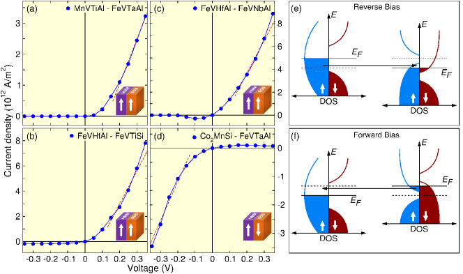
Finally, we would like to comment on the on/off ratios and current densities of the OSDs. The ratios at V vary between (FeVHfAlFeVTiSi) and (MnVTiAlFeVTaAl) at zero temperature. Since FeVTiSi possesses the largest overlap between the conduction and valence band edges of opposite spin channels around , the FeVHfAlFeVTiSi junction shows the largest leakage current as discussed above and thus the lowest on/off ratio. From that point of view, also the on/off current ratios can be increased by using materials with ideal spin-gapless semiconducting behavior. Here, the MnVTiAlFeVTaAl junction seems to be the best candidate for realizing the OSD. Another aspect that influences the on/off ratios is temperature, which is neglected in our transport calculations due to the technical limitation of the QuantumATK package for spintronic materials as discussed in Ref. 14. Temperature effects as well as the spin-flip excitations can further reduce the on/off current ratio in OSDs (see Ref. 14 for a detailed discussion). As for the current densities, the calculated values are comparable to the elementary metals and much higher than conventional or diodes [27, 28, 29, 30]. It is worth to note that in transport calculations within the QuantumATK package all inelastic scattering processes stemming from phonons as well as electrons and magnons are neglected. All these neglected processes can substantially reduce the current density of the OSDs.
In conclusion, the OSD is a recently proposed concept in spintronics and requires materials with unique electronic properties, in particular half-metallic and spin-gapless semiconducting behavior. Since both properties have already been identified in the family of ordered quaternary Heusler compounds, this family is a preferable choice for the realization of such devices. Moreover, most of the compounds within this family possess very high Curie temperatures making them potential candidates for spintronic applications at room temperature. By using first principles DFT calculations combined with the NEGF method, we proposed four different HMM-SGS junctions (or OSDs) within the family of quaternary Heusler compounds. All four OSDs show linear characteristics with zero threshold voltage in the on state and small leakage currents in the off state which can be attributed to the small overlap of conduction and valence band edges of opposite spin channels around the Fermi level in the SGS electrode. In three of the designed OSDs, the HMM and SGS electrodes couple ferromagnetically, while in the Co2MnSiFeVTaAl junction this coupling is antiferromagnetic and thus this diode can be configured dynamically via an external magnetic field. Furthermore, the zero threshold voltage is important for reducing the power consumption in a diode as it scales linearly with . We hope that our results pave the way for the experimental fabrication of OSDs based on quaternary Heusler compounds.
Acknowledgements.
This work was supported by the European Union (EFRE), Grant No: ZS/2016/06/79307 and by Deutsche Forschungsgemeinschaft (DFG) SFB CRC/TRR 227.Data availability
The data that support the findings of this study are available from the corresponding author upon reasonable request.
References
- De Groot et al. [1983] R. A. De Groot, F. M. Mueller, P. G. Van Engen, and K. H. J. Buschow, Phys. Rev. Lett. 50, 2024 (1983).
- Özdoğan, Şaşıoğlu, and Galanakis [2013] K. Özdoğan, E. Şaşıoğlu, and I. Galanakis, J. Appl. Phys. 113, 193903 (2013).
- Galanakis, Özdoğan, and Şaşıoğlu [2016] I. Galanakis, K. Özdoğan, and E. Şaşıoğlu, AIP Adv. 6, 055606 (2016).
- Gao, Opahle, and Zhang [2019] Q. Gao, I. Opahle, and H. Zhang, Phys. Rev. Mater. 3, 024410 (2019).
- Ouardi et al. [2013] S. Ouardi, G. H. Fecher, C. Felser, and J. Kübler, Phys. Rev. Lett. 110, 100401 (2013).
- Wang [2008] X. L. Wang, Phys. Rev. Lett. 100, 156404 (2008).
- Aull et al. [2019] T. Aull, E. Şaşıoğlu, I. V. Maznichenko, S. Ostanin, A. Ernst, I. Mertig, and I. Galanakis, Phys. Rev. Materials 3, 124415 (2019).
- Kämmerer et al. [2004] S. Kämmerer, A. Thomas, A. Hütten, and G. Reiss, Appl. Phys. Lett. 85, 79 (2004).
- Sakuraba et al. [2006] Y. Sakuraba, a. M. Hattori, M. Oogane, Y. Ando, H. Kato, A. Sakuma, T. Miyazaki, and H. Kubota, Appl. Phys. Lett. 88, 192508 (2006).
- Wang et al. [2009] W. Wang, H. Sukegawa, R. Shan, S. Mitani, and K. Inomata, Appl. Phys. Lett. 95, 182502 (2009).
- Xu et al. [2013] G. Z. Xu, E. K. Liu, Y. Du, G. J. Li, G. D. Liu, W. H. Wang, and G. H. Wu, Europhys. Lett. 102, 17007 (2013).
- Faleev et al. [2017] S. V. Faleev, Y. Ferrante, J. Jeong, M. G. Samant, B. Jones, and S. S. P. Parkin, Phys. Rev. Mater. 1, 024402 (2017).
- Şaşıoğlu, Blügel, and Mertig [2019] E. Şaşıoğlu, S. Blügel, and I. Mertig, ACS Appl. Electron. Mater. 1, 1552 (2019).
- Şaşıoğlu et al. [2020] E. Şaşıoğlu, T. Aull, D. Kutschabsky, S. Blügel, and I. Mertig, Phys. Rev. Appl. 14, 014082 (2020).
- Smidstrup et al. [2017] S. Smidstrup, D. Stradi, J. Wellendorff, P. A. Khomyakov, U. G. Vej-Hansen, M.-E. Lee, T. Ghosh, E. Jónsson, H. Jónsson, and K. Stokbro, Phys. Rev. B 96, 195309 (2017).
- Smidstrup et al. [2019] S. Smidstrup, T. Markussen, P. Vancraeyveld, J. Wellendorff, J. Schneider, T. Gunst, B. Verstichel, D. Stradi, P. A. Khomyakov, U. G. Vej-Hansen, M.-E. Lee, S. T. Chill, F. Rasmussen, G. Penazzi, F. Corsetti, A. Ojanperä, K. Jensen, M. L. N. Palsgaard, U. Martinez, A. Blom, M. Brandbyge, and K. Stokbro, J. Phys. Condens. Matter 32, 015901 (2019).
- Perdew, Burke, and Ernzerhof [1996] J. P. Perdew, K. Burke, and M. Ernzerhof, Phys. Rev. Lett. 77, 3865 (1996).
- Van Setten et al. [2018] M. J. Van Setten, M. Giantomassi, E. Bousquet, M. J. Verstraete, D. R. Hamann, X. Gonze, and G.-M. Rignanese, Comput. Phys. Commun. 226, 39 (2018).
- Büttiker et al. [1985] M. Büttiker, Y. Imry, R. Landauer, and S. Pinhas, Phys. Rev. B 31, 6207 (1985).
- Fuh et al. [2016] H.-R. Fuh, C.-R. Chang, Y.-K. Wang, R. F. Evans, R. W. Chantrell, and H.-T. Jeng, Sci. Rep. 6, 32625 (2016).
- Kuroda, Fukushima, and Oguchi [2020] F. Kuroda, T. Fukushima, and T. Oguchi, J. Appl. Phys. 127, 193904 (2020).
- Nikolaev et al. [2009] K. Nikolaev, P. Kolbo, T. Pokhil, X. Peng, Y. Chen, T. Ambrose, and O. Mryasov, Appl. Phys. Lett. 94, 222501 (2009).
- Bai et al. [2013] Z. Bai, Y. Cai, L. Shen, G. Han, and Y. Feng, Appl. Phys. Lett. 102, 152403 (2013).
- Sze and Ng [2007] S. M. Sze and K. K. Ng, Physics of Semiconductor Devices, 3rd ed. (John Wiley & Sons, Hoboken, 2007).
- Murali et al. [2018] K. Murali, M. Dandu, S. Das, and K. Majumdar, ACS Appl. Mater. Interfaces 10, 5657 (2018).
- Roy et al. [2015] T. Roy, M. Tosun, X. Cao, H. Fang, D.-H. Lien, P. Zhao, Y.-Z. Chen, Y.-L. Chueh, J. Guo, and A. Javey, ACS Nano 9, 2071 (2015).
- Harris, Walker, and Sneddon [1980] A. J. Harris, R. S. Walker, and R. Sneddon, J. Appl. Phys. 51, 4287 (1980).
- Gibson et al. [1980] R. A. Gibson, W. E. Spear, P. G. Le Comber, and A. J. Snell, J. Non-Cryst. Solids 35, 725 (1980).
- Szydlo et al. [1982] N. Szydlo, E. Chartier, N. Proust, J. Magarino, and D. Kaplan, Appl. Phys. Lett. 40, 988 (1982).
- Deng et al. [2003] J. Deng, J. M. Pearce, R. J. Koval, V. Vlahos, R. W. Collins, and C. R. Wronski, Appl. Phys. Lett. 82, 3023 (2003).