Modulation characteristics of uncooled graphene photodetectors
Abstract
We analyze the modulation characteristics of the uncooled terahertz (THz) and infrared (IR) detectors using the variation of the density and effective temperature of the two-dimensional electron-hole plasma in uniform graphene layers (GLs) and perforated graphene layers (PGLs) due to the absorption of THz and IR radiation. The performance of the photodetectors (both the GL-photoresistor and the PGL-based barrier photodiodes) are compared. Their characteristics are also compared with the GL reverse-biased photodiodes. The obtained results allow to evaluate the ultimate modulation frequencies of these photodetectors and can be used for their optimization.
I INTRODUCTION
The non-equilibrium two-dimensional electron-hole plasma (2DEHP) in graphene layers (GLs) from equilibrium 1 ; 2 ; 3 ; 4 ; 5 ; 6 ; 7 ; 8 ; 9 enables the operation of different GL-based terahertz (THz) and infrared (IR) electro-optical modulators, ultrafast thermal light sources with high carrier effective temperature, the superluminescent and lasing diodes, and, particularly, the hot/cool carrier bolometric detectors of electromagnetic radiation 10 ; 11 ; 12 ; 13 ; 14 ; 15 ; 16 ; 17 ; 18 ; 19 ; 20 . Such detectors use the effect of the conductivity variation due to the carrier density and effective temperature variation and the change associated with the radiation absorption. The speed (in particular, the maximum modulation frequency) of the GL-based photodetectors is one of their important characteristics. The maximum modulation frequency depends on not only the carrier energy relaxation and recombination, but also on the 2DEHP heat capacities. Despite a relatively small value of the latter compared to the heat capacity of the substrate and of the GL encapsulation layers in which GLs are encapsulated, it can limit the modulation speed.
In this paper, we study the modulation characteristics of the uncooled THz and IR GL hotodetectors using the effects of the interband carrier generation/recombination and the carrier heating/cooling (the bolometric mechanism). We account for the essential interdependence of these processes. We clarify of the relative roles of the carrier energy accumulation and the relaxation and recombination processes in the dynamic (modulation) properties of the uncooled (operating at room temperature) photodetectors. Our analysis accounts for the correct value of the 2DEHP capacity, which substantially deviates from its classical value.
The developed device model describes the high-speed operation of the photodetectors with uniform and perforated GLs.
II DEVICE MODEL AND GENERAL EQUATIONS
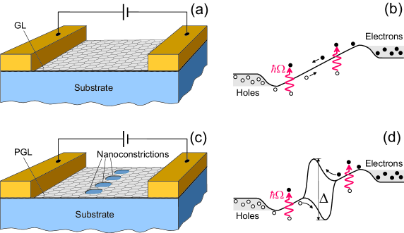
We consider the photodetectors based on the undoped GLs supplied by the side Ohmic (p- and n-) contacts. The Fermi levels in the contacts align with the GL Dirac points shifted, by the dc bias voltage . The GL regions can be either uniform (in the GL photoresistors) or comprise a perforated array in the perforated GL (PGL) barrier photodiodes. Figure 1 show the structures and the band diagrams of the devices under study. The normally incident THz or IR radiation absorbed in the GL results in the extra electron-hole pair generation and affects the energy of the 2DEHP. The variation of the carrier density and their effective temperature leads to the variation of the GL conductivity and the current through the PGL region and modulates the terminal current. In the perforation array, the carrier current flows only in the nanoconstrictions 21 ; 22 ; 23 ; 24 (GL quantum wires or nanoribbons) between the perforations. If the nanoconstrictions are sufficiently narrow, the quantization of the carrier energy spectrum results in the barriers for the carriers coming from the uniform parts of the GL, which limit the terminal current. The steady-state bolometric characteristics of the uniform GL and the GLs with the region patterned into the GL nanowires (nanoribbons) were evaluated previously 9 ; 12 . As it was predicted a long time ago 21 , the inclusion of the vertical and lateral barrier regions between the photosensitive standard quantum wells 25 ; 26 ; 27 and between the GLs in the GL-based hot-carrier bolometers with the vertical structure 28 ; 29 generally leads to the responsivity enhancement. The barriers between the carrier puddles and the lateral quantum dots in GLs 13 ; 16 can play a similar role.
The 2DEHP density and effective temperature are determined by radiation absorption and the interband (recombination) and intraband relaxation processes.
Due to relatively frequent carrier-carrier collisions in the GLs at room temperatures, the 2DEHP electron and hole subsystems can be described by quasi-Fermi energy distribution functions and with common effective temperature (in energy units) : , . Here is the carrier kinetic energy and and are the electron and hole quasi-Fermi energies, respectively. Due to a symmetry of the electron and hole subsystems in the situations under consideration, . In the equilibrium (without an external irradiation), . Generally, the absorption of the incident radiation can lead to , although, except for the cases of a strong irradiation, .
Limiting our consideration to the room temperatures, we assume that the main mechanisms of the density and energy relaxation are associated with the GL optical phonons 30 ; 31 ; 32 .
The pertinent rate equations, which govern the density and energy balances in the 2DEHP, are given by
| (1) |
| (2) |
Here and are the net carrier density and the carrier energy per unit square, respectively, in the entire GL or its parts separated by the constriction area, , , , and are the pertinent rates of the electron-hole pair generation by the incoming radiation and the interband and intraband transitions with the generation and absorption of optical phonons, and the Auger recombination-generation processes 9 ; 33 ; 34 ; 35 , respectively, and are the photon and optical phonon energies ( meV), and is the Planck constant. The right-hand side of Eq. (2) reflects the fact that each absorbed photon increases the 2DEHP energy by a quantity , while the absorption and emission of optical phonons change this energy by . The Auger processes affect the carrier density, however, due to the zero energy gap, they do not vary the 2DEHP energy. The explicit expressions for the relaxation terms , , and are given (exemplified) in the Appendix A.
The dispersion relations for electrons (upper sign) and holes (lower sign) in the GLs are presented as
| (3) |
where cm/s is the characteristic carrier velocity in GL , is the carrier momentum. Hence, for the rate of the electron-hole pairs photogeneration we arrive at the following formulas:
| (4) |
Here , and are the electron charge and light speed, respectively, is the dielectric constant of the layers surrounding the GL, is the 2DEHP temperature. The normally incident radiation flux, , comprises the steady-state component and the modulation signal component :
where and are the amplitude and the frequency of the modulated signal.
The absorption the THz and IR photons in GLs is due to the interband (mainly direct optical transitions) and to the intraband (indirect transitions). At the photon frequencies , where is the carrier momentum relaxation time, the latter mechanism, which corresponds to the carrier Drude absorption, is relatively weak and, for simplicity, it is disregarded in Eq. (3) (although this mechanism was included into our model previously 9 ). The carrier densities and their energy densities as functions of the effective temperature and the quasi-Fermi energy are given in the Appendix B, Eq. (B1).
The GL conductivity is determined by the carrier densities, i.e., by the quasi-Fermi energy , and by their effective temperature . Assuming that the GL dc and low signal frequency conductivities, are determined by the short-range scattering (on the defects and acoustic phonons), so that (for GLs) 3 ; 9 , where is the characteristic short-range scattering time 36 , one can obtain the following formula:
| (5) |
Here is the intrinsic conductivity in the dark condition: and . At relatively weak irradiation, , and Eq. (5) yields
| (6) |
According to Eq. (6), the terminal photocurrent across the uniform GL, , between the side contacts in the GL photoresistors can be presented as
| (7) |
so that its value normalized by the dark currents is given by
| (8) |
Here is the spacing between the contacts and is the GL width in the direction perpendicular to the current.
The nanoconstriction 21 ; 22 constitutes a 1D channel for electrons and holes (quantum wires or nanoribbons 37 ; 38 ; 39 ). Considering that the energy gap in the nanoconstriction as a function of the coordinate along the carrier propagation direction is determined by the nanoconstriction length and width, and , respectively, and the voltage drop between the nanoconstriction edges : , can be presented as (if ) with . For an effective control of the net current the height of the barrier (i.e., the energy gap ) should be sufficiently large to provide relatively small voltage drop across the uniform regions in the GL and GBL. In this case, , where is the bias voltage between the side contacts. Accounting for this, the ratio of the net thermionic photocurrents currents, and , in the photodiodes based on the perforated GLs (PGLs) over the barriers in the nanoconstriction 22 , can be presented as
| (9) |
One can see from the comparison of Eqs. (8) and (9) that the relative variations of the net currents under the irradiation in the case of the perforated GLs comprise the factor , which can be large for sufficiently narrow nanoconstrictions.
III STEADY-STATE CARRIER QUASI-FERMI ENERGY, EFFECTIVE TEMPERATURE, and DC PHOTOCURRENT
At , Eqs. (1) - (3) with Eqs. (A1) and (B1) result in the following values of the steady-state components of the quasi-Fermi energies and the effective temperature :
| (10) |
| (11) |
Here , , , is the 2DEHP density at , is the characteristic time of the Auger carrier generation, is the rate of the electron-hole pair generation in GLs due to the absorption of equilibrium optical phonons cm-2s-1 21 . At meV, and ps.
Equations (10) and (11) show that depending on the ratio , the quasi-Fermi energies and the deviation of the effective temperatures from the lattice temperature can be both positive and negative. The radiation frequencies, at which the quasi-Fermi energies change their signs are the same (), while the change of the signs of and occurs at somewhat different .
Omitting the term due to its smallness (see Appendix A), the dc photocurrents in the GL photoresistor and PGL photodiode can be presented as
| (12) |
| (13) |
Equation (12) coincides with the pertinent formula obtained previously 9 for the case of the short-range carrier scattering. The expression for the GL photoconductivity given by Eq. (12) does not explicitly comprises the term associated with the variation of the effective temperature, i.e., the bolometric term. However, the variation of the quasi-Fermi energy and, particularly, the possible change of this quantity sign at a certain ratio , is related to the 2DEHP heating (or cooling). This implies that the bolometric effect in the GL photoresistors plays a role, although implicitly. In contrast to the GL photoconductivity, the expression for the PGL photoconductivity explicitly comprises the term associated with the bolometric effect. The bolometric contribution is proportional to a small parameter . The presence of the energy barrier in the constrictions area, the value of the photocurrent in the PGL photodiode in comparison with the GL photoresistor is proportional to a large factor .
As seen from Eqs. (12) and (13), the dc photoconductivity changes the sign at a certain ratio . This is because at a large , the radiation absorption leads to the 2DEHP heating that results in a lowering of the electron quasi-Fermi level (it goes below the Dirac point to the valence band) and in a elevating of the hole quasi- Fermi level (which appears in the conduction band), while at , the radiation absorption can give rise to the 2DEHP cooling and, hence, to .
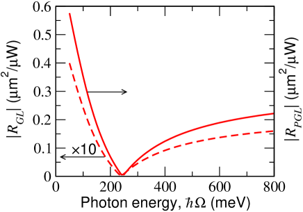
Figure 2 shows the spectral characteristics of the GL photoresistor and PGL photodiode normalized dc responsivities, and , calculated using Eqs. (12) and (13). We set , , and meV (the nanoconstrictions with nm).
The most remarkable feature of the spectral characteristics of and seen in Fig. 2 is that these values turn to zero at a certain ratio . This is associated with the equality of the energy received by the 2DEHP from the absorbed radiation and the energy transmitted to the optical phonons when . As follows from Eqs. (10) and (11), at the latter relation, and become equal to zero, that leads to the zero values of the photocurrent.
IV MODULATED QUASI-FERMI ENERGY, EFFECTIVE TEMPERATURE, AND AC PHOTOCURRENT
When the incident radiation comprises the ac modulation component , we arrive at the following equations for the ac components of the quasi-Fermi energy and effective temperature, and :
| (14) |
| (15) |
which in the limit convert into Eqs. (10) and (11), respectively. The characteristic times , , and are given in the Tables I and II and are being proportional to the time related to the electron-hole pair generation rate associated with the optical phonon absorption in GLs. Assuming that cm-2s-1 at meV, for (weak Auger processes) we obtain ps. The carrier heat capacity (per one carrier) [see Appendix B, Eq. B(6)]
The times and are the effective carrier recombination and cooling/heating times, respectively. The inclusion of the Auger recombination leads to a decrease in the recombination time . One can see that is proportional to the product of the heat capacitance per one carrier and the carrier energy relaxation time due to the interaction with optical phonons (that is in line with the previous calculation of this time in the 2D systems 4 ). Despite a relatively short time , it is longer than one could assume in the case of the classical value (see the Appendix B).
For the 2DEHP in the GL, the hierarchy of the characteristic times is as follows: . One can see from Eqs. (14) and (15) that substantially depends on . In particular, an increase in leads to a decrease in . Equations (14) and (15) result in
| (16) |
| (17) |
where
| (18) |
GL, PGL
(ps) (ps) (ps) GL, PGL 35 – 70 21 – 42 7 – 14
Calculating the ac components of the ac photocurrent current as in the previous section, we arrive at the following equation:
| (19) |
Analogously, invoking Eq. (9), for the ac photocurrent in the PGL photodiodes we obtain
| (20) |
V MODULATION DEPTH
The modulation depths normalized by the dark currents (in units m2/W) can be defined as
| (21) |
for the GL photoresistors and the PGL photodiodes, respectively.
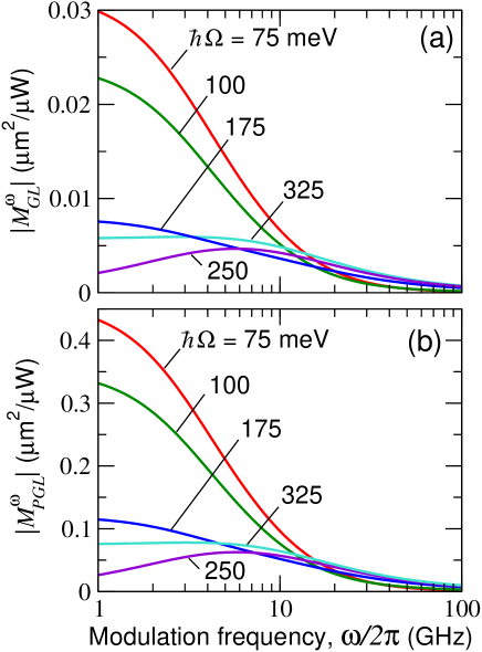
Figure 3 shows the absolute value (modulus) of the modulation depths and as functions of the modulation frequency calculated using Eqs. (21) with Eqs. (19) and (20) for different carrier frequencies (different photon energies ). It is assumed that cm-2s-1 and, hence, ps, ps, ps , and ps (see Table II). Other parameters are the same, as in Fig. 2, namely, , , and meV.
In the range of the photon energies, i.e., the carrier frequencies . the modulation depth decreases with the modulation frequencies exceeding several GHz. At , a marked decrease in and takes place starting at more than 10 GHz.
It is interesting that at , the dependences of and on the modulation frequency exhibit maxima at about several MHz at which and exceed and . This can be explained by a change in the phase shift between the quasi-Fermi and the effective temperature oscillations with a change of the modulation frequency.
VI COMMENTS
VI.1 Comparison of GL and PGL photodetectors
Using Eqs. (8), (9), (13), (14), (19), and (20), we can arrive at the following ratios of the photocurrents normalized by the dark currents in the GL photoresistors and the PGL photodiodes:
| (22) |
VI.2 Comparison of GL and PGL photodetectors with reverse-biased GLD photodiodes
The photocurrents in the GL photodetectors under consideration and in the p-i-n photodiodes 41 at a reverse strong bias providing the depletion of the GL with not too long absorbing GL (with the spacing between the side contact , where is the drift length) can be estimated as follows 41 :
| (23) |
The dark current associated with the carrier generation due to the interband absorption of optical phonons in the GLDs is given by
| (24) |
Using Eq. (12), for the ratios of the dc photocurrents (detector responsivities) normalized by the dark currents we obtain
| (25) |
| (26) |
One can see from Eq. (25) that at , i.e., in the THz and far-IR spectral ranges . If (mid- and near-IR ranges), can markedly exceed unity. Due to a large factor , can be particularly large in a wide spectral range. Indeed, if, for example, meV and meV, Eq. (26) yields .
The GL-photoresistor and PGL photodiode responsivities and can be derived using Eqs. (12) and (13):
| (27) |
| (28) |
Assuming cm-2s-1, ps, m, and mV for meV, we find A/W. For this photon energy, one obtains A/W. Setting m and , for the same voltage and photon energy, we obtain A/W. If meV (corresponding to a smaller than in the above estimate of ), one obtains A/W. These estimates show that the PGL photodiodes can surpass the GLD photodiodes in the parameter because of low values of the dark current, exhibiting, however, the responsivities of the same order of magnitude.
VI.3 Role of Auger processes
Due to a smallness of the parameter , the Auger processes weakly affect the characteristics of the photodetectors under consideration. This in particular, implies that despite a weak temperature dependence of the uniform GL conductivity, its photoresponse can be marked due to the deviation of the quasi-Fermi levels from the Dirac point cased by the 2DEHP heating or cooling. This is contrast to the situation when a relatively dense 2DEHP is hot 42 ; 43 ; 44 ; 45 ; 46 ; 47 ; 48 ; 49 ; 50 , so that the Auger processes in GLs are rather effective 34 . The latter forces the quasi-Fermi levels be very close to the Dirac point () 51 .
VI.4 Assumptions
The screening lengths in GLs with can be estimated as 51
| (29) |
For , from Eq. (22) we obtain nm This length is much smaller than the characteristic carrier wave lengths nm.
This justifies the assumption of our model that the ionized impurities are effectively screened, so that the carrier scattering on such impurities, point defects, and acoustic phonons is a short-range scattering.
In Eq. (2) we used the quantity given by Eq. (4). The latter ignores the contribution of the intraband photon absorption by the carriers (the Drude absorption). This is justified if (see, for example, 9 )
| (30) |
where stands for the Drude factor. Inequality (30) yields the following condition:
| (31) |
For meV and ps, one obtains meV. The photon energies assumed in the above calculations are much larger. The generalization of our model for smaller is rather simple.
The biased voltage can lead to some 2DEHP Joule heating. Considering that the Joule power in the GL per unit of its area , one can find the condition that the pertinent variation of the 2DEHP temperature if the electric field across the GL . For the parameters used in the above estimates V/cm.
Above we assumed that the operation of the PGL photodiode is determined by the variations of the current across the nanoconstrictions. Considering the voltage drop across the constriction area and the uniform GL region, the PGL photodiode net resistance can be expressed as
| (32) |
Here is given by Eq. (5) and
is the resistance of the perforated area for a parabolic potential distribution along the nanoconstrictions [see Eq. (13) in 22 ] with being the number of the nanoconstrictions. Hence, the variation of the nanoconstriction resistance (assumed above) is much larger than that of the uniform parts of the GL if
| (33) |
i.e.,
| (34) |
Setting m, m, (m) and ps or and ps, for meV we find that, according to inequality (33), a marked distinction in the GL and PGL photodetectors requires meV.
VII CONCLUSIONS
We developed analytical models for the uncooled GL and PGL photodetectors. Their operation is linked to the correlated variations of the carrier density (i.e., quasi-Fermi energies) and effective temperature associated with the interband absorption of the incident modulated radiation. We derived the modulation characteristic as a function of the carrier and modulation frequencies, demonstrated that the variation of both the carrier density and the effective temperature are essential for the GL- and PGL-based photodetectors, and showed that the value 2DEHP capacity (markedly different form the classical value) affects the response time. The comparison of photodetectors under consideration showed that the presence of the energy barrier for the carriers in the nanoconstrictions in the PGL photodiodes promotes the higher photodetectors performance. We also compared the the GL- and PGL-based photodetectors with the interband photodiodes with the reverse-bias depleted GL. As shown the former can surpass the latter somewhat slower devices.
ACKNOWLEDGMENTS
The Japan Society for Promotion of Science (KAKENHI 16H06361), Japan; RIEC Nation-Wide Collaborative Research Project H31/A01), Japan; the Russian Foundation for Basic Research (Grant 18-29-02089), Russia; the Office of Naval Research, USA; the US Army Research Laboratory Cooperative Research Agreement, USA.
DATA AVAILABILITY
The data that support the findings of this study are available from the corresponding author upon reasonable request.
Appendix A. The density and energy relaxation rates
The rates of the interband and intraband processes involving the optical phonons can be presented as:
| (A1) |
and
| (A2) |
Here is the rate of the electron-hole pair generation due to the absorption of equilibrium optical phonons in the GLs, the quantities is the ratio of the rates of the intraband and interband transitions in the GLs accompanied by the absorption of an optical phonon. This quantity is mainly determined by the energy dependences of the densities of states around the Dirac point. For GLs, at , 4 .
According to the calculation 30 , at meV, for the intra-valley and inter-valley optical phonons in GLs, cm-2s-1 21 . The characteristic time of the interband transitions with absorption of an optical phonon can be defined as , where .
The rates of the Auger recombination-generation processes are assumed in the following form:
| (A3) |
where is the rate of the electron-hole pair generation due to the impact Auger processes in the 2DEHP with the equilibrium carrier density. In GLs these processes are characterized by so that . Since the time of the carrier recombination due to the spontaneous optical phonon emission . The characteristic time can be estimated as . Setting ps 34 , we find that the parameter ps, so that , i.e., fairly small.
Appendix B. GL carrier and energy densities versus carrier quasi-Fermi energy and effective temperature
The net carrier (electrons and holes) densities in the GL in line with Eq. (2) is given by
| (B1) |
The density of the carrier energy in the 2DEHP can be calculated as
| (B2) |
In the undoped GLs, the electron and hole densities are equal to each other. In this case, due to a symmetry of the valence and conduction bands, . Except the situations when GLs and GBLs are strongly optically or injection pumped with the generation of cold or warm carriers, . In such cases, Eqs. (B1) and (B2) yield 40
| (B3) |
| (B4) |
where is the Riemann zeta function: .
Considering that the 2DEHP heat capacity in GLs is defined as , from Eq. (B4) we obtain
| (B5) |
so that the 2DEHP capacity, (in units of the Boltzmann constant ), per one carrier is given by
| (B6) |
This value is markedly different from the classical value for nondegenerate 2D systems 40 .
References
- (1) V. Ryzhii, M. Ryzhii, and T. Otsuji, “Negative dynamic conductivity of graphene with optical pumping,”J. Appl. Phys. 101, 083114 (2007).
- (2) F. T. Vasko and V. Ryzhii, “Photoconductivity of intrinsic graphene,”Phys. Rev. B 77, 195433 (2008).
- (3) A. Satou, F. T. Vasko, and V. Ryzhii, “Nonequilibrium carriers in intrinsic graphene under interband photoexcitation,”Phys. Rev. B 78 , 115431 (2008).
- (4) V. Ryzhii, M. Ryzhii,V. Mitin, A. Satou, and T. Otsuji, “Effect of heating and cooling of photogenerated electron-hole plasma in optically pumped graphene on population inversion,”Jpn. J. Appl. Phys. 50, 094001 (2011).
- (5) S. Boubanga-Tombet, S. Chan, T. Watanabe, A. Satou, V. Ryzhii, and T. Otsuji, “Ultrafast carrier dynamics and terahertz emission in optically pumped graphene at room temperature,”Phys. Rev. B 85, 035443 (2012).
- (6) T. Li, L. Luo, M. Hupalo, J. Zhang, M. C. Tringides, J. Schmalian, and J.Wang, “Femtosecond population inversion and stimulated emission of dense Dirac fermions in graphene,”Phys. Rev. Lett. 108, 167401 (2012).
- (7) I. Gierz, J. C. Petersen, M. Mitrano, C. Cacho, I. E. Turcu, E. Springate, A. Stöhr, A. Köhler, U. Starke, and A. Cavalleri, “Snapshots of non-equilibrium Dirac carrier distributions in graphene,”Nat. Mater. 12, 1119 (2013).
- (8) J. N. Heyman, J. D. Stein, Z. S. Kaminski, A. R. Banman, A. M. Massari, and J. T. Robinson, “Carrier heating and negative photoconductivity in graphene,”J. Appl. Phys. 117, 015101 (2015).
- (9) V. Ryzhii, D. S. Ponomarev, M. Ryzhii, V. Mitin, M. S. Shur, and T. Otsuji, “Negative and positive terahertz and infrared photoconductivity in uncooled graphene,”Opt. Mat. Express 9, 585 - 597 (2019).
- (10) M. Shur, A.V. Muraviev, S. L. Rumyantsev, W. Knap, G. Liu, and A. A. Balandin, “Plasmonic and bolometric terahertz graphene sensors,”Proc. of 2013 IEEE Sensors Conf., 978-1- 4673-4642-9/13/ 2013 IEEE pp. 1688-1690 (2013).
- (11) J. Yan, M.-H. Kim, J. A. Elle, A.B. Sushkov, G.S. Jenkins, H.M. Milchberg, 3, M.S. Fuhrer, and H.D. Drew, “Dual-gated bilayer graphene hot electron bolometer,”Nat. Nanotech. 7, 472–478 (2012).
- (12) V. Ryzhii, T. Otsuji, M. Ryzhii, N. Ryabova, S. O. Yurchenko, V. Mitin, and M. S. Shur, “Graphene terahertz uncooled bolometers,”J. Phys. D: Appl. Phys. 46, 065102 (2013).
- (13) Q Han, T. Gao, R. Zhang, Y. Chen, J.Chen, G. Liu, Y. Zhang, Z. Liu, X. Wu, and D. Yu, “Highly sensitive hot electron bolometer based on disordered graphene,”Sci. Reports 3, 3533 (2013).
- (14) X. Cai, A. B. Sushkov, R J. Suess, M. M. Jadidi, G. S. Jenkins, L. O. Nyakiti, R. L. Myers-Ward, S. Li, J. Yan, D. K. Gaskill, T. E. Murphy, H. D. Drew, and M. S. Fuhrer, “Sensitive room-temperature terahertz detection via the photothermoelectric effect in graphene,”Nat. Nanotech. 9, 814-819 (2014).
- (15) X. Du, D. E. Prober, H. Vora, and Ch. B. Mckitterick, “Graphene-based bolometers,”Graphene 2D Mater. 1, 1-22 (2014).
- (16) A. El Fatimy, R. L. Myers-Ward, A. K. Boyd, K. M. Daniels, D. K. Gaskill, and P. Barbara, “Epitaxial graphene quantum dots for high-performance terahertz bolometers,”Nat. Nanotechnol. 11, 335-338 (2016).
- (17) S. Yuan, R. Yu, C. Ma, B. Deng, Q. Guo, X. Chen, C. Li, C. Chen, K. Watanabe, T. Taniguchi, F. J. García de Abajo, and F. Xia, “Room temperature graphene mid-infrared bolometer with a broad operational wavelength range,”ACS Photonics 7, 1206-1215 (2020).
- (18) V. Ryzhii, M. Ryzhii, D. Ponomarev, V. G. Leiman, V. Mitin, M. Shur, and T. Otsuji, “Negative photoconductivity and hot-carrier bolometric detection of terahertz radiation in graphene-phosphorene hybrid structures,”J. Appl. Phys. 125, 151608 (2019).
- (19) A. Blaikie, D. Miller, and B. J. Alemán, “A fast and sensitive room-temperature graphene nanomechanical bolometer,”Nat. Comm. 10, 4726 (2019).
- (20) G.-H. Lee, D. K. Efetov, L. Ranzani, E. Walsh, J. Crossno, T. A. Ohki, T. Taniguchi, K. Watanabe, P. Kim, D. Englund, and K. C. Fong, “Graphene-based Josephson junction microwave bolometer,”Nature 586, 42 – 46 (2020).
- (21) G. S. Simin, M. Islam, M. Gaevski, J. Deng, R. Gaska, and M. S. Shur, “Low RC-constant perforated-channel HFET,”IEEE Electron Device Lett. 35, 452-454 (2014).
- (22) V. Ryzhii, M. Ryzhii, M. S. Shur, V. Mitin, A. Satou, and T. Otsuji, “Resonant plasmonic terahertz detection in graphene split-gate field-effect transistors with lateral p-n junctions, ”J. Phys. D: Appl. Phys. 49, 315103 (2016).
- (23) R. P. Panmand, P.Patil, Y Sethi, S. R. Kadam, M. V. Kulkarni,S. W. Gosavi, N. R. Munirathran, and B. B. Kale, “Unique perforated graphene derived fromBougainvilleaflowers for high-powersupercapacitors: a green approach,”Nanoscale 9, 4801 (2017).
- (24) A. Guirguisa, J. W. Maina, L. Kong, L. C. Henderson, A. Rana, L. H. Li, M. Majumder, L. F. Dumee, “Perforation routes towards practical nano-porous graphene andanalogous materials engineering ”Carbon 155, 660 (2019).
- (25) R. A. Suris and V. A. Fedirko, “Heating photoconductivity in a semiconductor with a superlattice,”Sov. Phys. Semicond. 12, 629 (1978).
- (26) E. A. Shaner, A. D. Grine, M. C. Wanke, M. Lee, J. R. Reno, and S. J. Allen, “Far-infrared spectrum analysis using plasmon modes in a quantum-well transistor, ”IEEE Photonics Technol. Lett. 18, 1925 (2006).
- (27) V. Ryzhii, A. Satou, T. Otsuji, and M. S. Shur, “Plasma mechanism of resonant terahertz detection in a two-dimensional electron channel with split gates,”J. Appl. Phys. 103, 014504 (2008).
- (28) V. Ryzhii, A. Satou, T. Otsuji, M. Ryzhii, V. Mitin, and M. S. Shur, “Graphene vertical hot-electron terahertz detectors,”J. Appl. Phys. 116, 114504 (2014).
- (29) M. Ryzhii, V. Ryzhii, V. Mitin, M. S. Shur, and T. Otsuji, “Vertical hot-electron terahertz detectors based on black-As1-xPx/graphene/black-As1-xPx heterostructures,”Sensors and Materials 31, 2271-2279 (2019).
- (30) F. Rana, P. A. George , J. H. Strait, S. Sharavaraman, M. Charasheyhar, and M. G. Spencer, “Carrier recombination and generation rates for intravalley and intervalley phonon scattering in graphene,”Phys. Rev. B 79, 115447 (2009).
- (31) H. Wang, J. H. Strait, P. A. George, S. Shivaraman, V. D. Shields, M. Chandrashekhar, J. Hwang, F. Rana, M. G. Spencer, C. S. Ruiz-Vargas, and J. Park, “Ultrafast relaxation dynamics of hot optical phonons in graphene,”Appl. Phys. Lett. 96, 081917 (2010).
- (32) J. M. Iglesias, M. J. Martín, E. Pascual, and R. Rengel, “Hot carrier and hot phonon coupling during ultrafast relaxation of photoexcited electrons in graphene,”Appl. Phys. Lett. 108, 043105 (2016).
- (33) M. S. Foster and I. L. Aleiner, “Slow imbalance relaxation and thermoelectric transport in graphene,”Phys. Rev. B 79, 085415 (2009).
- (34) G. Alymov, V. Vyurkov, V. Ryzhii, A. Satou, and D. Svintsov, “Auger recombination in Dirac materials: A tangle of many-body effects,”Phys. Rev. B 97, 205411 (2018).
- (35) V. Ryzhii, T. Otsuji, M. Ryzhii, V. E. Karasik, and M. S. Shur, “Negative terahertz conductivity and amplification of surface plasmons in graphene–black phosphorus injection laser heterostructures,”Phys. Rev. B 100 115436 (2019).
- (36) A. Shik, Quantum Wells: Physics and Electronics of Two-Dimensional systems (World Scientific Singapore, 1997)
- (37) V. V. Mitin, D. I. Sementsov, and N. Vagidov, Quantum Mechanics for Nanostructures (Cambridge Univ. Press, Cambridge, 2010).
- (38) G. Liang, N. Neophytou, M. S. Lundstrom, and D E. Nikonov, “Contact effects in graphene nanoribbon transistors,”Nano Lett. 8, 1819-1824 (2008).
- (39) K.-T. Lam and G. Liang, “Electronic structure of bilayer graphene nanoribbon and its device application: A computational study,”NanoSci. and Technol. 57, 509-527 (2012).
- (40) V. Ryzhii, M. Ryzhii, T. Otsuji, V. Mitin, and M. S. Shur, “Heat capacity of nonequilibrium electron-hole plasma in graphene layers and graphene bilayers,”arXiv:2011.03739 [cond-mat.mes-hall].
- (41) V. Ryzhii, M. Ryzhii, V. Mitin, and T. Otsuji, “Terahertz and infrared photodetection using p-i-n multiple-graphene layer structures,”J. Appl. Phys. 107, 054512 (2010).
- (42) M. Freitag, H.-Y. Chiu, M. Steiner, V. Perebeinos, and P. Avouris, ”Thermal infrared emission from biased graphene,” Nat. Nanotech. 5, 497–501 (2010).
- (43) Y. D. Kim, H. Kim, Y. Cho, Ji H. Ryoo, C.-H. Park, P. Kim, Y. S. Kim, S. Lee, Y. Li, S.-N. Park, Y. S. Yoo, D. Yoon, V. E. Dorgan, E. Pop, T. F. Heinz, J. Hone, S.-H. Chun, H. Cheong, S. W. Lee, M.-Ho Bae, and Y. D. Park, “Bright visible light emission from graphene,”Nat. Nanotech. 10, 676–681 (2015).
- (44) H. R.Barnard, E. Zossimova, N. H. Mahlmeister, L. M. Lawton, I. J. Luxmoore, and G. R. Nash, “Boron nitride encapsulated graphene infrared emitters,”Appl. Phys. Lett. 108, 131110 (2016).
- (45) S.-K. Son, M. S̆ i s̆ kins, C. Mullan, J. Yin, V. G. Kravets, A. Kozikov, S. Ozdemir, M. Alhazmi, M. Holwill, K. Watanabe, T. Taniguchi, D. Ghazaryan, K. S. Novoselov, V. I. Fal’ko, and A. Mishchenko, “Graphene hot-electron light bulb: incandescence from hBN encapsulated graphene in air, ”2D Materials 5, 011006 (2017).
- (46) H. M. Dong, W. Xu, and F. M. Peeters, “Electrical generation of terahertz blackbody radiation from graphene,”Opt. Express 26(19), 24621–24626 (2018).
- (47) R.-J. Shiue, Y. Gao, C. Tan, C. Peng, J. Zheng, D. K. Efetov, Y. D. Kim, J. Hone, and D. Englund, “Thermal radiation control from hot graphene electrons coupled to a photonic crystal nanocavity,”Nat. Commun. 10, 109 (2019).
- (48) F. Luo, Y. Fan, G. Peng, S. Xu, Y. Yang, K. Yuan, J. Liu, W. Ma, W. Xu, Z. H. Zhu, X.-Ao Zhango, A. Mishchenko, Yu Ye, H. Huang, Z. Han, W. Ren, K. S. Novoselov, M. Zhu, and S. Qin, “Graphene thermal emitter with enhanced Joule heating and localized light emission in air,”ACS Photonics 6, 2117–2125 (2019).
- (49) Y. D. Kim, Y. Gao, R.-J. Shiue, L. Wang, O. B. Aslan, M.-Ho Bae, H. Kim, D. Seo, H.-J. Choi, S. H. Kim, A. Nemilentsau, T. Low, C. Tan, D. K. Efetov, T. Taniguchi, K. Watanabe, K. L. Shepard, T. F. Heinz, D. Englund, and J. Hone, “Ultrafast graphene light emitters,”Nano Lett. 18, 934–940 (2018).
- (50) V. Ryzhii, T. Otsuji, M. Ryzhii, V. Leiman, P. P. Maltsev, V. E. Karasik, V. Mitin, and M. S. Shur, “Theoretical analysis of injection driven thermal light emitters based on graphene encapsulated by hexagonal boron nitride,”Opt. Mat. Express 11, 468 (2021).
- (51) V. Ryzhii, M. Ryzhii, D. Svintsov, V. Leiman, P. P. Maltsev, D. S. Ponomarev, V. Mitin, M. S. Shur, and T. Otsuji, “Real-space-transfer mechanism of negative differential conductivity in gated graphene-phosphorene hybrid structures: Phenomenological heating model,”J. Appl. Phys. 124, 114501 (2018).