Coexistence of intrinsic piezoelectricity and nontrivial band topology in monolayer InXO (X=Se and Te)
Abstract
The combination of piezoelectricity with other unique properties (like topological insulating phase and intrinsic ferromagnetism) in two-dimensional (2D) materials is much worthy of intensive study. In this work, the piezoelectric properties of 2D topological insulators InXO (X=Se and Te) from monolayer InX (X=Se and Te) with double-side oxygen functionalization are studied by density functional theory (DFT). The large piezoelectric strain coefficients (e.g. =-13.02 pm/V for InSeO and =-9.64 pm/V for InTeO) are predicted, which are comparable and even higher than ones of many other familiar 2D materials. Moreover, we propose two strategies to enhance piezoelectric response of monolayer InXO (X=Se and Te). Firstly, the biaxial strain (0.94-1.06) is applied, and the (absolute value) is increased by 53%/56% for monolayer InSeO/InTeO at 1.06 strain, which is due to increased (absolute value) and reduced . In considered strain range, InXO (X=Se and Te) monolayers are always 2D topological insulators, which confirm the coexistence of piezoelectricity and nontrivial band topology. Secondly, a Janus monolayer is designed by replacing the top Se/Te atomic layer in monolayer InSeO/InTeO with Te/Se atoms, which is dynamically and mechanically stable. More excitingly, Janus monolayer is also a 2D topological insulator with sizeable bulk gap up to 0.158 eV, confirming the coexistence of intrinsic piezoelectricity and topological nature. The calculated is -9.9 pm/V, which is in the middle of ones of InSeO and InTeO monolayers. Finally, the carrier mobilities of monolayer InXO (X=Se and Te) are obtained, which shows a rather pronounced anisotropy between electron and hole, and are almost isotropic between armchair and zigzag directions. Our works imply that it is possible to use the piezotronic effect to control the quantum transport process, ultimately leading to novel device applications in monolayer InXO (X=Se and Te), and can stimulate further experimental works.
pacs:
71.20.-b, 77.65.-j, 72.15.Jf, 78.67.-n Email:sandongyuwang@163.comI Introduction
2D materials can show a variety of extraordinary new physical properties, like 2D piezoelectricity and quantum spin Hall (QSH) phase. The piezoelectricity allows for energy conversion between electrical and mechanical energy, and a 2D material should break inversion symmetry, and then can exhibit piezoelectricity, which has attracted growing interest due to potential application in sensors, actuators and energy sourcesq4 . The monolayer with 2H phase is predicted as a typical 2D piezotronic materialq11 , and then is proved to possess piezoelectricity experimentally with =2.9 C/mq5 ; q6 . In theory, the piezoelectric properties of many 2D materials have been reported by DFT calculationsq11 ; q7 ; q9 ; q10 ; q12 ; q13 ; q14 ; q15 ; q16 ; q17 , like transition metal dichalchogenides (TMD), Janus TMD, group IIA and IIB metal oxides, group III-V semiconductors, family, and group-III monochalcogenides.
Topological insulators have rich physics and promising applications in spintronics and quantum computationst1 ; t2 . The QSH insulators are a novel quantum state, which can be characterized by the gapless edge states inside the bulk gap. The charge carriers from edge states are robust against backscattering, which is very useful for energy-efficient electronic devices. The QSH insulators are known as 2D topological insulators, which is firstly proposed in graphenet3 , and are experimentally verified in HgTe/CdTe and InAs/GaSb quantum wellst4 ; t5 . Many QSH insulators have been theoretically proposedt6 ; t7 ; t8 ; t9 ; t10 ; cxq , such as silicene, Bi(111) bilayer, chemically modified Sn, / , and .
Compared with 2D materials with individual piezoelectric or QSH characteristics, 2D piezoelectric topological insulators with both piezoelectric and QSH characteristics will open up unprecedented opportunities for intriguing physics, whose exploitation will ultimately lead to novel device applications. The combination of piezoelectricity and ferromagnetism has been achieved in 2D vanadium dichalcogenides and septuple-atomic-layer qt1 ; q15 , and a 2D ferroelastic topological insulator that simultaneously possesses ferroelastic and QSH characteristics has also been predicted in 2D Janus TMD MSSe (M = Mo and W)qt2 . However, to the best of our knowledge, no studies have been reported on combination of piezoelectricity and QSH insulators.
The group-III monochalcogenides with broken inversion symmetry have piezoelectricityq16 , and the piezoelectricity of Janus group-III chalcogenide monolayers can be enhanced with respect to perfect group-III monochalcogenide. monolayersq17 . Recently, monolayer group-III monochalcogenides by oxygen functionalization are predicted as a promising class of 2D topological insulatorsqt3 , which break inversion symmetry, allowing these materials to become piezoelectric. In this work, the piezoelectric properties of monolayer InXO (X=Se and Te) are reported by using DFT. The large of monolayer InXO (X=Se and Te) are predicted, and they are -13.02 pm/V for InSeO and -9.64 pm/V for InTeO. The biaxial strain is used to tune their piezoelectric properties, and the improvement is by 53%/56% for monolayer InSeO/InTeO at 1.06 strain. Inspiring from experimentally synthesized MoSSe monolayermsse , a Janus monolayer with dynamical and mechanical stability is designed, and it is a 2D topological insulator with the gap value of 0.158 eV. The predicted is -9.99 pm/V, which falls between ones of InSeO and InTeO monolayers. In all our studied systems, the coexistence of piezoelectricity and nontrivial band topology is confirmed, which may provide a new platform for intriguing physics and novel device applications.
The rest of the paper is organized as follows. In the next section, we shall give our computational details and methods. In the next few sections, we shall present crystal and electronic structures, piezoelectric properties, strain and Janus effects on piezoelectric properties, and carrier mobilities of monolayer InXO (X=Se and Te). Finally, we shall give our discussion and conclusions.
| / | |||
|---|---|---|---|
| 4.46 (4.78) | 27.13 (24.85) | 11.21 (9.57) | 7.96 (7.64) |
| 22.50 (21.17) | 0.41 (0.39) | 0.096 (0.163) | 1(1) |

II Computational detail
The first-principles calculations within DFT1 are performed using the projected augmented wave (PAW) method, as implemented in the VASP packagepv1 ; pv2 ; pv3 . The cutoff energy for plane-wave expansion is 500 eV, and the vacuum region along the z direction is set to about 20 in order to to avoid interactions between two neighboring images. The popular generalized gradient approximation of Perdew, Burke and Ernzerhof (GGA-PBE)pbe is used as the exchange-correlation potential. The spin-orbit coupling (SOC) is included to study electronic structures and piezoelectric stress coefficients . K-point meshes of 16161 are employed for geometry optimization and self-consistent electronic structure calculations. The total energy convergence criterion is set to eV. The geometry optimization was considered to be converged with the residual force on each atom being less than 0.0001 .
To obtain the piezoelectric strain coefficients , the elastic stiffness tensor are calculated by using strain-stress relationship (SSR), and the piezoelectric stress coefficients are calculated by density functional perturbation theory (DFPT) methodpv6 . The 2D elastic coefficients and piezoelectric stress coefficients have been renormalized by the the length of unit cell along z direction (): = and =. The Brillouin zone sampling is done using a Monkhorst-Pack mesh of 16161 for , and 5101 for . The invariants are calculated by the Wannier90 and WannierTools codesw1 ; w2 , where a tight-binding Hamiltonian with the maximally localized Wannier functions is fitted to the first-principles band structures. We use Phonopy codepv5 to calculate phonon dispersion spectrums of monolayer with a supercell of 551. The finite displacement method is adopted, and a 221 k-mesh is employed with kinetic energy cutoff of 500 eV.
| Name | |||||
| InSe | -0.69 (-0.57q16 , -0.70q17 ) | 49.74 (51q16 , 55q17 ) | 13.55(12q16 , 20q17 ) | 36.20 | -1.92 (-1.46q16 , -1.98q17 ) |
| InSeO | -2.07 | 27.13 | 11.21 | 15.92 | -13.02 |
| InTe | -0.53(-0.69q17 ) | 41.23 (64q17 ) | 10.43(6q17 ) | 30.80 | -1.73 (-1.18q17 ) |
| InTeO | -1.47 | 24.85 | 9.57 | 15.28 | -9.64 |
| Name | InSe | InSeO | InTe | InTeO |
|---|---|---|---|---|
| Ele | -5.14 | -5.44 | -4.55 | -4.18 |
| Ion | 4.44 | 3.37 | 4.02 | 2.71 |
III Crystal and electronic structures
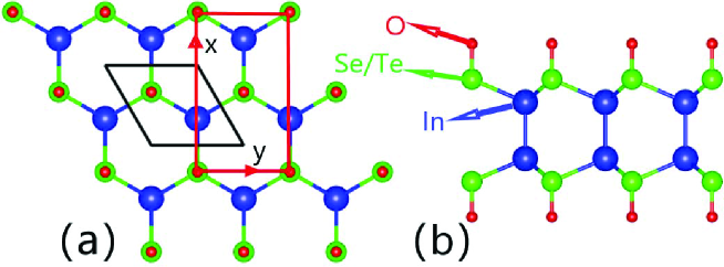
The crystal structure of monolayer InXO (X=Se and Te) can be constructed from monolayer InX (X=Se and Te) by oxygen functionalization with chemisorption of oxygen atoms on both sides. Monolayer InX (X=Se and Te) has a hexagonal lattice, which is composed of two In atomic layers sandwiched between X atomic layers. The geometric structure of monolayer InXO (X=Se and Te) is shown in Figure 1, and both rhombus primitive cell and rectangle supercell are plotted. The rectangle supercell is used to calculate carrier mobilities and piezoelectric coefficients with armchair and zigzag directions be defined as x and y directions. The monolayer InXO (X=Se and Te) has the same point group with g- and gsd . The optimized lattice constant of monolayer InSeO and InTeO are 4.46 and 4.78 , and the bond length between O and X atoms is 1.67 and 1.84 , which agree well previous theoretical valuesqt3 . It is found that the lattice constants of monolayer InXO are larger than ones of monolayer InX (InSe:4.09 and InTe:4.38 ) due to oxygen functionalization.
In ref.qt3 , it is proved that monolayer InXO (X=Se and Te) possess energetic, thermal and chemical stabilities. Here, we further check the mechanical stability of the monolayer InXO (X=Se and Te) by elastic constants . Using Voigt notation, the elastic tensor can be expressed as:
| (1) |
The two independent elastic constants of monolayer InSeO/InTeO are =27.13 /24.85 and =11.21 /9.57 . The can be attained by (-)/2, and they are 7.96 /7.64 , which are also shear modulus . The mechanical stability of a material with hexagonal symmetry should satisfy the Born criteriaela :
| (2) |
The calculated and confirm the mechanical stability of monolayer InXO (X=Se and Te). The Young’s modulus are givenela1 :
| (3) |
where . Due to hexagonal symmetry, the monolayer InXO (X=Se and Te) are mechanically isotropic. The calculated is 22.50 /21.17 for InSeO/InTeO monolayer. These values are obviously smaller than those of other 2D materialsq11 ; q7 ; q9 ; q10 ; q12 ; q13 ; q14 ; q15 ; q16 ; q17 , which means that InSeO and InTeO monolayers are more flexible than other 2D materials. The Poisson’s ratio is also isotropic, and can be expressed as:
| (4) |
The calculated is 0.41/0.39 for InSeO/InTeO monolayer.
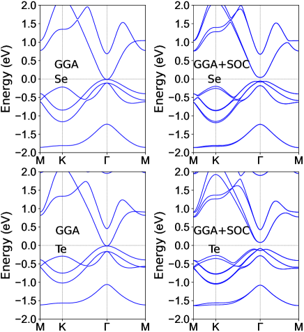
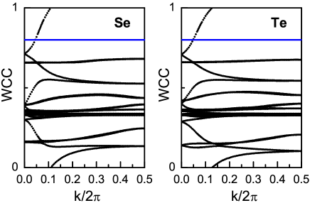
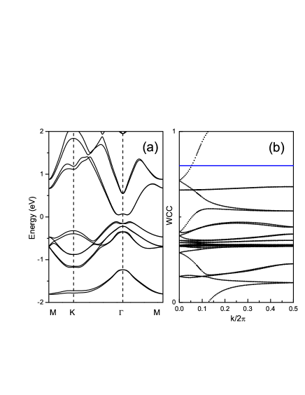
The energy bands of monolayer InXO (X=Se and Te) with GGA and GGA+SOC are shown in Figure 2. The GGA results show that the monolayer InXO (X=Se and Te) are semimetals with the valence band maximum (VBM) and conduction band minimum (CBM) degenerated at the point. When the SOC is included, a direct gap of 0.096 eV/0.163 eV is observed for InSeO/InTeO monolayer. The transition from semimetal to insulator induced by SOC suggests that InXO (X=Se and Te) monolayers are potential 2D topological insulators. In order to ascertain the topological phase transition in the monolayer InXO (X=Se and Te), we calculate the topological invariants with = 1 being a topologically nontrivial state and = 0 being a trivial state. Since the InXO (X=Se and Te) monolayers lack inversion symmetry, the invariants cannot be determined from the parities of the filled states. However, the topologically nontrivial nature can be confirmed via calculations of the Wannier charge center (WCC), as plotted in Figure 3. It is clearly seen that the number of crossings between the WCC and the reference horizontal line is odd, which confirms the topological nature of monolayer InXO (X=Se and Te) with = 1.
IV Piezoelectric properties
The pristine InX (X=Se and Te) monolayers are piezoelectricq16 , and their piezoelectric effect can be enhanced by designing Janus structuresq17 . When the InX (X=Se and Te) monolayers with both sides are fully covered by O atoms [InXO (X=Se and Te) monolayers], they have the same point group symmetry with InX monolayers, which is because the O-X bonds are perpendicular to the InX layers. Therefore, InXO (X=Se and Te) monolayers are also piezoelectric. The piezoelectric effects of a material can be described by third-rank piezoelectric stress tensor and strain tensor from the sum of ionic and electronic contributions, which are defined as:
| (5) |
and
| (6) |
In which , and are polarization vector, strain and stress, respectively. The / is clamped-ion piezoelectric coefficients, while the / is relax-ion piezoelectric coefficients as a realistic result.
For 2D materials, ==0 for i=3 or j=3q9 ; q10 ; q11 ; q12 . Due to a point-group symmetry of InXO (X=Se and Te) monolayers, the piezoelectric stress and strain tensors with Voigt notation can be reduced into:
| (7) |
| (8) |
where / represents the in-plane piezoelectric stress/strain component, which is induced by uniaxial in-plane strain. The can be calculated by DFPT, and the can be attained by the relation:
| (9) |
Here, the is derived by Equation 7, Equation 8, Equation 9 and Equation 1:
| (10) |
The orthorhombic supercell as the computational unit cell is used to calculate by DFPT. The calculated in-plane () of monolayer InSeO and InTeO are -2.07 C/m (-13.02 pm/V) and -1.47 C/m (-9.64 pm/V). The (absolute values) of monolayer InXO (X=Se and Te) is much higher than those of the widely used bulk piezoelectric materialsaln ; aln-1 ; aln-2 ; aln-3 such as -quartz (=2.3 pm/V), wurtzite-AlN (=5.1 pm/V) and wurtzite-GaN (=3.1 pm/V). Their are also comparable to or even superior than ones of many familiar 2D materialsq7 ; q9 ; q11 ; q12 ; q7-2 ; q7-1 , such as (=3.65 pm/V), (=2.12 pm/V), ZnO (=8.65 pm/V), MoSSe (=3.76 pm/V) and MoSTe (=5.04pm/V). It is found that the (absolute values) of monolayer InXO (X=Se and Te) is comparable to or even smaller than ones of (=3.62 C/m ), (=2.43 C/m ), ZnO (=2.66 C/m ), MoSSe (=3.74 C/m ) and MoSTe (=4.53 C/m )q7 ; q9 ; q7-2 ; q7-1 , but their are larger than ones of those monolayers. The underlying reason is that the of monolayer InXO (X=Se and Te) is very smaller than ones of (49.7 )q9 , (57.2 )q9 , ZnO (15.4 )q9 , MoSSe (49.7 )q7 and WSTe (45 )q7 , which leads to larger based on Equation 10 (The is inversely proportional to .). These results show that monolayer InXO (X=Se and Te) may have large in-plane piezoelectric response, when a uniaxial strain is applied.
To consider oxygen functionalization effects on piezoelectric properties, the piezoelectric coefficients of pristine InX (X=Se and Te) monolayers also are calculated, and their , and along with previous theoretical values are listed in Table 2. Our calculated results agree with previous available onesq16 ; q17 . Upon double-side functionalization, the are improved as well to -2.07 C/m/-1.47 C/m from -0.69 C/m/-0.53 C/m for monolayer InSeO/InTeO, and the are reduced to 15.92 /15.28 from 36.20 /30.80 . These give rise to enhanced piezoelectric effect by oxygen functionalization. Finally, the ionic and electronic contributions to of monolayer InXO and InX (X=Se and Te) are listed in Table 3. It is clearly seen that the ionic and electronic contributions are opposite for all four monolayers, and the electronic contribution dominates the . Compared to monolayer InX(X=Se and Te), the oxygen functionalization can lead to small difference between the ionic and electronic contributions for monolayer InXO (X=Se and Te), which induces the larger . Thus, it is very important for calculating to use relaxed-ion, not clamped-ion.
| Carrier type | () | () | (eV) | () | ||
|---|---|---|---|---|---|---|
| Electrons | x | 22.50 | 0.799 | -8.56 | 10.21 | |
| InSeO | y | 22.50 | 0.804 | -8.57 | 10.13 | |
| Holes | x | 22.50 | -0.428 | -8.59 | 35.50 | |
| y | 22.50 | -0.427 | -8.58 | 35.66 | ||
| Electrons | x | 21.17 | 0.538 | -8.47 | 21.38 | |
| InTeO | y | 21.17 | 0.555 | -8.47 | 20.73 | |
| Holes | x | 21.17 | -0.245 | -8.54 | 100.77 | |
| y | 21.17 | -0.256 | -8.53 | 96.66 |
V Strain effects
Strain is a very effective method to tune piezoelectric properties of 2D materialsgsd ; s1 ; s2 ; s3 , and the of monolayer and g- with the same space group (No. 187) of monolayer InXO (X=Se and Te) can be improved by biaxial tensile strain. Compared to unstrained one, tensile strain of 4% can raise the of /g- by about 46%/330%gsd . So, it is very interesting to investigate biaxial strain effects on piezoelectric properties of monolayer InXO (X=Se and Te). For space group (No. 187), the biaxial strain can not produce polarization, but the uniaxial strain along x or y direction can induce polarization charges. Here, we only consider biaxial strain ( from 0.94 to 1.06) effects on piezoelectric properties of monolayer InXO (X=Se and Te).
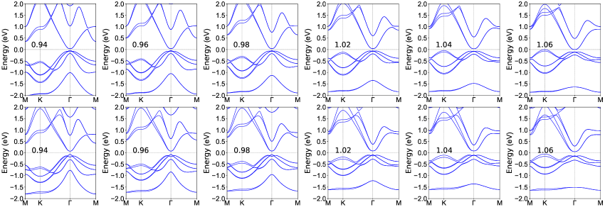
At applied strain, the monolayer InXO (X=Se and Te) should be a semiconductor to exhibit piezoelectricity, and the strain-related energy bands are plotted in Figure 4. It is clearly seen that monolayer InXO (X=Se and Te) during the whole strain range all have a gap, and the SOC gap never closes, which means that the nontrivial topology is robust under considered compressive/tensile strains. To precisely confirm coexistence of intrinsic piezoelectricity and nontrivial band topology, the topological invariants are calculated for all considered ones, and they all satisfy =1. Here, we only show the fitted energy band of monolayer InSeO by Wannier90 and evolution of the WCC of monolayer InSeO at 1.06 strain in Figure 5. These mean that the piezoelectricity can coexist with nontrivial band topology in all considered strained monolayer InXO (X=Se and Te).
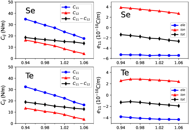
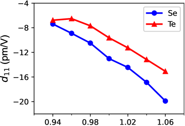
The elastic constants , piezoelectric coefficients along the ionic and electronic contributions, and of monolayer InXO (X=Se and Te) as a function of strain are plotted in Figure 6 and Figure 7. With the strain from 0.94 to 1.06, all monotonously decrease, and the reduced is in favour of improving according to Equation 10. It is found that piezoelectric coefficient (absolute values) increases with strain from 0.94 to 1.06, which can give rise to enhanced . At 1.06 strain, the of InSeO/InTeO reaches up to -19.91 pm/V/-15.08 pm/V from unstrained -13.02 pm/V/-9.64 pm/V, increased by 53%/56%. Thus, tensile strain can improve piezoelectric response of monolayer InXO (X=Se and Te).
VI Janus structure
By constructing the Janus structure, the piezoelectric response () of the pristine InX (X=Se and Te) monolayers can be enhancedq17 . The of can be improved to 4.73 pm/V from 1.98 pm/V of InSe or 1.18 pm/V of InTeq17 . It’s a natural idea to achieve Janus 2D monolayer from monolayer InXO (X=Se and Te). To construct the Janus structure, the monolayer can be achieved by replacing the top Se/Te atomic layer in monolayer InSeO/InTeO with Te/Se atoms. The symmetry of monolayer (No.156) is lower than that of the monolayer InXO (X=Se and Te) (No.187) due to the lack of the reflection symmetry with respect to the central In atomic bilayer. The reduced symmetry can induce many novel properties, like out-of-plane piezoelectric polarizations.
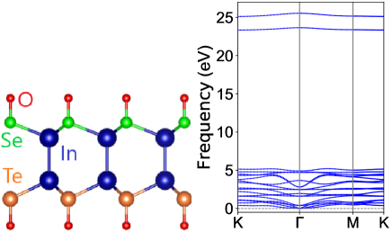
The side view of crystal structure of monolayer is shown in Figure 8, along with its phonon band dispersions. The optimize lattice constants are ==4.63 , which is between ones of InSeO and InTeO. The bond lengths of monolayer between O and Se/Te atoms is 1.67 /1.84 , which is the same with one of monolayer InSeO/InTeO. The phonon dispersions show no imaginary bands, signifying its dynamic stability. The out-of-plane vibration of the O atoms are at frequency of 23 eV-26 eV, and there are two phonon bands due to inequitable O atoms of both sides, which is different from one of InSeO or InTeOqt3 . The other phonon bands are below 5.3 eV. The calculated elastic constants satisfy the Born criteria of mechanical stability with =25.85 and =10.46 . The other elastic physical quantities are calculated, such as =7.69 , =21.62 and =0.41.
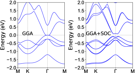
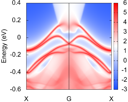
The energy band structures of monolayer using GGA and GGA+SOC are shown in Figure 9. The SOC can induce that monolayer changes from semimetal to insulator (the gap of 0.158 eV), which suggests that it may be a potential topological insulator. To confirm the topologically nontrivial character of the gap, we further evaluate the invariant by tracing the evolution of the WCC, which is shown in Figure 10 along with the fitted energy band of monolayer by Wannier90. The invariant is identified by the odd number crossings of WCC (black lines) of the reference line (blue line), and the =1, which indicates that the monolayer is a 2D topological insulator, possessing the helical edge states connecting the conduction and valence bands. And, we use Green’s-function method to calculate the surface states on (100) surface based on the tight-binding Hamiltonian, which is plotted in Figure 11. Clearly, the edge states of monolayer are present in the energy gap.
The monolayer InXO (X=Se and Te) [ symmetry] possess a reflection symmetry with respect to the central In atomic bilayer, which requires that /=0. In monolayer , the inequivalent Se-In and Te-In bonding lengths break the reflection symmetry along the vertical direction, resulting in a low degree of symmetry. And then, both / and / are nonzero. The piezoelectric stress and strain tensors will become into:
| (11) |
| (12) |
According to above discussions, when a uniaxial in-plane strain is applied, both monolayer InXO (X=Se and Te) and have in-plane piezoelectric polarization, but monolayer has an additional vertical piezoelectric polarization. When they are subject to biaxial in-plane strain, the in-plane piezoelectric polarization will be suppressed for both monolayer InXO (X=Se and Te) and , while the out-of-plane one still will remain in monolayer . Based on Equation 11, Equation 12, Equation 9 and Equation 1, the and can be expressed as:
| (13) |
The calculated of monolayer is -1.54 C/m from the the ionic contribution 2.98 C/m and electronic contribution -4.52 C/m. Based on Equation 13, the calculated is -9.99 pm/V, which falls between ones of the InSeO and InTeO. Similar phenomenon can be found in TMD and familiesq7 ; gsd1 . For example, the of the Janus (M=Mo and W) monolayers are between those of the (M=Mo and W) and (M=Mo and W) monolayersgsd1 . The predicted is up to 26.25 pm/V due to very large of 9.53 C/m, which is mainly from ionic contribution (93%). The more accurate calculation with a 7121 k-mesh confirms the very large .
VII Carrier mobility
Finally, we also investigate the carrier mobilities of electron/hole of monolayer InXO (X=Se and Te) by the deformation potential (DP) theory proposed by Bardeen and Shockleydp , and the carrier mobility of a 2D material () can be expressed as:
| (14) |
where the electron charge, the reduced Planck constant and the Boltzmann constant are marked by , and , and the temperature, effective mass in the transport direction and the average effective mass are shown by the and and . In addition, represents the DP constant, as defined by , where can be calculated by the band edge of CBM or VBM minus the vacuum level. The strain range is chose from -0.01 to 0.01 with the step =0.005.
The rectangular supercell is used to calculate the carrier mobilities of monolayer InXO (X=Se and Te) with the temperature being 300 K. Firstly, the effective masses of CBM and VBM along x and y directions are calculated by:
| (15) |
where is the dispersion of the lowest conduction band/the highest valence band. To fit second-order polynomial , the 4 k points with a spacing of 0.003 reciprocal lattice constants are used to produce the inverse mass tensor. It is found that the effective masses of holes of monolayer InXO (X=Se and Te) are smaller than ones of electrons, and the effective masses between x and y directions for both electrons and holes are very close. The DP constant can be attained by linearly fitting the band energies of the VBM and CBM with respect to the vacuum energy, and the related slopes are DP constant . Calculated results show that all of both the VBM and CBM of both monolayer InSeO and InTeO almost are the same, and about -8.5.
Based on Equation 14, the carrier mobilities of monolayer InXO (X=Se and Te) are attained, which are shown Table 4. The hole mobilities of monolayer InXO (X=Se and Te) are in the range of 35.50-100.77 , which are larger than those of electrons (10.13-21.38 ). This is because the holes have smaller effective masses than electrons. It is found that the carrier mobilities of both electrons and holes between x and y directions show very weak anisotropy, which is because the effective masses and between x and y directions are very close.
VIII Discussions and Conclusion
Due to expensive computation time to calculate and using hybrid functional HSE06 or HSE06+SOC, we use GGA or GGA+SOC to investigate the and of monolayer InXO (X=Se and Te). Although the GGA may underestimate semiconductor gaps of monolayer InXO (X=Se and Te), our conclusion should be qualitatively correct. The intrinsic piezoelectricity and nontrivial band topology can coexist in Janus monolayer . In fact, Janus monolayer and are all topological insulators, and they can also achieve coexistence of intrinsic piezoelectricity and nontrivial band topology.
In summary, we demonstrate piezoelectric QSH insulators in monolayer InXO (X=Se and Te) by using first-principles calculations. The biaxial strain and constructing Janus structure are used to tune piezoelectric properties of monolayer InXO (X=Se and Te). It is found that tensile strain can effectively improve the of monolayer InXO (X=Se and Te), and the strained systems are all QSH insulators. The Janus monolayer is predicted to be a QSH insulator with sizable nontrivial band gap, which is dynamically and mechanically stable. The calculated of monolayer is between ones of monolayer InSeO and InTeO. The unique coexistence of piezoelectricity and QSH insulator in monolayer InXO (X=Se and Te) along with offers the opportunities for achieving multi-function control electronic devices. Our work will inspire further researches to explore piezoelectric QSH insulators.
Acknowledgements.
This work is supported by Natural Science Basis Research Plan in Shaanxi Province of China (2019JQ-860). We are grateful to the Advanced Analysis and Computation Center of China University of Mining and Technology (CUMT) for the award of CPU hours and WIEN2k/VASP software to accomplish this work.References
- (1) W. Wu and Z. L. Wang, Nat. Rev. Mater. 1, 16031 (2016).
- (2) K. N. Duerloo, M. T. Ong and E. J. Reed, J. Phys. Chem. Lett. 3, 2871 (2012).
- (3) W. Wu, L. Wang, Y. Li, F. Zhang, L. Lin, S. Niu, D. Chenet, X. Zhang, Y. Hao, T. F. Heinz, J. Hone and Z. L. Wang, Nature 514, 470 (2014).
- (4) H. Zhu, Y. Wang, J. Xiao, M. Liu, S. Xiong, Z. J. Wong, Z. Ye, Y. Ye, X. Yin and X. Zhang, Nat. Nanotechnol. 10, 151 (2015).
- (5) L. Dong, J. Lou and V. B. Shenoy, ACS Nano, 11, 8242 (2017).
- (6) M. N. Blonsky, H. L. Zhuang, A. K. Singh and R. G. Hennig, ACS Nano, 9, 9885 (2015).
- (7) R. X. Fei, We. B. Li, J. Li and L. Yang, Appl. Phys. Lett. 107, 173104 (2015).
- (8) Y. Chen, J. Y. Liu, J. B. Yu, Y. G. Guo and Q. Sun, Phys. Chem. Chem. Phys. 21, 1207 (2019).
- (9) S. D. Guo, Y. T. Zhu, W. Q. Mu and W. C. Ren, EPL 132, 57002 (2020).
- (10) S. D. Guo, Y. T. Zhu, W. Q. Mu, L. Wang and X. Q. Chen, Comp. Mater. Sci. 188, 110223 (2021)
- (11) S. D. Guo, W. Q. Mu, Y. T. Zhu and X. Q. Chen, Phys. Chem. Chem. Phys. 22, 28359 (2020).
- (12) W. B. Li and J. Li, Nano Res. 8, 3796 (2015).
- (13) Y. Guo, S. Zhou, Y. Z. Bai, and J. J. Zhao, Appl. Phys. Lett. 110, 163102 (2017).
- (14) M. Z. Hasan and C. L. Kane, Rev. Mod. Phys. Kane, 82, 3045 (2010).
- (15) X. L. Qi and S. C. Zhang, Rev. Mod. Phys. 83, 1057 (2011).
- (16) C. L. Kane and E. J. Mele, Phys. Rev. Lett. 95, 226801 (2005).
- (17) M. Konig, S. Wiedmann, C. Brune et al., Science 318, 766 (2007).
- (18) I. Knez, R. R. Du and G. Sullivan, Phys. Rev. Lett. 107, 136603 (2011).
- (19) C. C. Liu, W. Feng, Y. Yao, Phys. Rev. Lett. 107, 076802 (2011).
- (20) S. Murakami, Phys. Rev. Lett. 97, 236805 (2006).
- (21) Y. Xu, B. Yan, H. J. Zhang et al., Phys. Rev. Lett. 111, 136804 (2013).
- (22) H. M. Weng, X. Dai and Z. Fang, Phys. Rev. X 4, 011002 (2014).
- (23) J. J. Zhou, W. X. Feng, C. C. Liu, S. Guan and Y. G. Yao, Nano Lett. 14, 4767 (2014).
- (24) L. Wang, Y. P. Shi, M. F. Liu et al., arXiv:2008.02981 (2020).
- (25) J. H. Yang, A. P. Wang, S. Z. Zhang, J. Liu, Z. C. Zhong and L. Chen, Phys. Chem. Chem. Phys., 21, 132 (2019).
- (26) Y. D. Ma, L. Z. Kou, B. B. Huang, Y. Dai and T. Heine, Phys. Rev. B 98, 085420 (2018).
- (27) S. Zhou, C. C. Liu, J. J. Zhao and Y. G. Yao, npj Quant. Mater. 3, 16 (2018).
- (28) A. Y. Lu, H. Y. Zhu, J. Xiao et al., Nature Nanotechnology 12, 744 (2017).
- (29) P. Hohenberg and W. Kohn, Phys. Rev. 136, B864 (1964); W. Kohn and L. J. Sham, Phys. Rev. 140, A1133 (1965).
- (30) G. Kresse, J. Non-Cryst. Solids 193, 222 (1995).
- (31) G. Kresse and J. Furthmller, Comput. Mater. Sci. 6, 15 (1996).
- (32) G. Kresse and D. Joubert, Phys. Rev. B 59, 1758 (1999).
- (33) J. P. Perdew, K. Burke and M. Ernzerhof, Phys. Rev. Lett. 77, 3865 (1996).
- (34) X. Wu, D. Vanderbilt and D. R. Hamann, Phys. Rev. B 72, 035105 (2005).
- (35) Q. Wu, S. Zhang, H. F. Song, M. Troyer and A. A. Soluyanov, Comput. Phys. Commun. 224, 405 (2018).
- (36) A. A. Mostofia, J. R. Yatesb, G. Pizzif, Y.-S. Lee, I. Souzad, D. Vanderbilte and N. Marzarif, Comput. Phys. Commun. 185, 2309 (2014).
- (37) A. Togo, F. Oba, and I. Tanaka, Phys. Rev. B 78, 134106 (2008).
- (38) S. D. Guo, W. Q. Mu and Y. T. Zhu, J. Phys. Chem. Solids 151, 109896 (2021).
- (39) R. C. Andrew, R. E. Mapasha, A. M. Ukpong and N. Chetty, Phys. Rev. B 85, 125428 (2012).
- (40) E. Cadelano, P. L. Palla, S. Giordano and L. Colombo, Phys. Rev. B 82, 235414 (2010).
- (41) K. Tsubouchi and N. Mikoshiba, IEEE Trans. Sonics Ultrason. SU-32, 634 (1985).
- (42) C. M. Lueng, H. L. Chang, C. Suya and C. L. Choy, J. Appl. Phys. 88, 5360 (2000).
- (43) A. Hangleiter, F. Htzel, S. Lahmann and U. Rossow, Appl. Phys. Lett. 83, 1169 (2003).
- (44) S. Muensit, E. M. Goldys and I. L. Guy, Appl. Phys. Lett. 75, 3965 (1999).
- (45) S. D. Guo, X. S. Guo, R. Y. Han and Y. Deng, Phys. Chem. Chem. Phys. 21, 24620 (2019).
- (46) M. Yagmurcukardes, C. Sevik and F. M. Peeters, Phys. Rev. B 100, 045415 (2019).
- (47) N. Jena, Dimple, S. D. Behere and A. D. Sarkar, J. Phys. Chem. C 121, 9181 (2017).
- (48) Dimple, N. Jena, A. Rawat, R. Ahammed, M. K. Mohanta and A. D. Sarkar, J. Mater. Chem. A 6, 24885 (2018).
- (49) S. D. Guo, X. S. Guo, Y. Y. Zhang and K. Luo, J. Alloy. Compd. 822, 153577 (2020).
- (50) S. D. Guo, W. Q. Mu, Y. T. Zhu, R. Y. Han and W. C. Ren, J. Mater. Chem. C, 2021, DOI: 10.1039/D0TC05649A.
- (51) S. Bruzzone and G. Fiori, Appl. Phys. Lett. 99, 222108 (2011).