Semiconductor-to-metal transition in bilayer MoSi2N4 and WSi2N4 with strain and electric field
Abstract
With exceptional electrical and mechanical properties and at the same time air-stability, layered MoSi2N4 has recently draw great attention. However, band structure engineering via strain and electric field, which is vital for practical applications, has not yet been explored. In this work, we show that the biaxial strain and external electric field are effective ways for the band gap engineering of bilayer MoSi2N4 and WSi2N4. It is found that strain can lead to indirect band gap to direct band gap transition. On the other hand, electric field can result in semiconductor to metal transition. Our study provides insights into the band structure engineering of bilayer MoSi2N4 and WSi2N4 and would pave the way for its future nanoelectronics and optoelectronics applications.
Since the discovery of graphene,Novoselov et al. (2004, 2005a, 2005b) there has been great research interests in two-dimensional (2D) layered materials due to their exceptional fundamental physical properties and tremendous potentials in devices applications.Bhimanapati et al. (2015); Tan et al. (2017) Owing to their high carrier mobility, excellent on/off ratio and unique optoelectronic properties, 2D transition metal dichalcogenides (TMD)Mak et al. (2010); Radisavljevic et al. (2011); Splendiani et al. (2010) and black phosphoreneLiu et al. (2014); Li et al. (2014); Koenig et al. (2014); Qiao et al. (2014) have been widely studied in last decade. To fully utilized those semiconducting 2D layered materials in nanoelectronics and optoelectronic devices, band gap engineering is indispensable and plays an essential role in device applications. One of the effective ways of tuning band gap is to apply strain to the layered materials. By doing so, electronic properties of TMD and phosphorene can be altered and strain sensitive device can be designed and fabricated.Johari and Shenoy (2012); Yun et al. (2012); Bhattacharyya and Singh (2012); Pan and Zhang (2012); Guo et al. (2014); Rodin et al. (2014); Peng et al. (2014); Fei and Yang (2014) The other strategy to achieve band gap engineering is by applying an external electric field, which may reduce the band gap for bilayer system and even lead to semiconductor to metal transition.Ramasubramaniam et al. (2011); Liu et al. (2012); Chu et al. (2015); Dolui et al. (2012); Kou et al. (2012); Liu et al. (2015); Wu et al. (2015); Huang et al. (2015); Cao et al. (2019)
Most recently, layered 2D MoSi2N4 and WSi2N4 has been experimentally synthesized using chemical vapor deposition (CVD).Hong et al. (2020) Experimental results suggest that they have semiconducting characteristic with good mechanical strength and air-stability. The paper also reported an intrinsic electron and hole mobilities of 270 cm2V-1s-1 and 1200 cm2V-1s-1, respectively, for layered 2D MoSi2N4, which is around four times as that of MoS2.Hong et al. (2020) With higher carrier mobility than MoS2 and better air-stability than phosphorene, MoSi2N4 and its family structure of MA2Z4 monolayers (M represents an early transition metal, A is Si or Ge, Z stands for N, P or As) have soon received much attention.Novoselov (2020); Tang et al. (2020); Li et al. (2020); Cao et al. (2021); Guo et al. (2020a, b); Mortazavi et al. (2020); Bafekry et al. (2020); Yang et al. (2020); Yu et al. (2020); Kang and Lin (2020); Wang et al. (2020) Nevertheless, there is still lack of band gap engineering study of bilayer MoSi2N4 and WSi2N4, which is critical for the future application of layered MA2Z4 material in nanoelectronics and optoelectronic devices up to date.
In this work, we explore the tuning of electrical band structure of bilayer MoSi2N4 and WSi2N4 under strain and external electric field. We find that band gaps can be tuned by both compress and tensile strain, which is a result of the change in Mo/W-N bond length and Mo-Mo/W-W distance induced by strain. We also find that the electric field can modulate the band gap, due to the charge redistribution induced by the electric field. Our findings imply that the strain and electric field tunable bilayer MoSi2N4 and WSi2N4 could be promising materials for the next generation nanoelectronics and optoelectronics.
Our first-principles study is carried out based on the density functional theory (DFT) calculations. The Vienna Ab initio Simulation Package (VASP)Kresse and Furthmüller (1996, 1996) was adopted for the geometry optimization and the QuantumATKSmidstrup et al. (2019) was used to investigate the electronic properties of bilayer MoSi2N4 and WSi2N4 under strain and external electric field. A gamma-centered Brillouin zone -point sampling grid using the Monkhorst-Pack methodMonkhorst and Pack (1976) of was used for geometry optimization and a grid of for property calculations. Atomic geometry optimization criteria is that all forces are smaller than 0.01 eV/Å. The generalized gradient approximation (GGA) with the Perdew-Burke-Ernzerhof form (PBE)Perdew et al. (1996) was chosen for the exchange-correlation functional in the calculations. The Heyd-Scuseria-Ernzerhof hybrid functional method (HSE)Heyd et al. (2003) was also used to obtain the more accurate band structure of the bilayers. To take into account the weak van der Waals interactions in the bilayers, we adopted the DFT-D3 method with the Grimme schemeGrimme et al. (2010, 2011) in the calculations. A 20 Å thick of vacuum layer was inserted between adjacent bilayers to eliminate the interactions from periodic images.Wu et al. (2019)
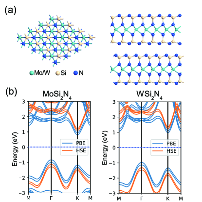
Based on our total energy calculations and also previous results,Hong et al. (2020) the AC stacking of the bilayer MoSi2N4 and WSi2N4 is the most stable bilayer configuration with the lowest total energy. Therefore, we only focus on the AC stacking in the following discussions. Figure 1(a) depicts the optimized geometric structure of the bilayer MoSi2N4 and WSi2N4. Our calculated lattice parameter of the bilayer MoSi2N4 and WSi2N4 is Å, which is in good agreement with previous calculated results.Hong et al. (2020) As shown in Fig. 1(b) the band structure of the bilayer MoSi2N4 and WSi2N4 is very similar to its monolayer counterpart with only small splitting in energy bands induced by the interlayer interactions, which slightly reduces the band gap. The indirect band gap of the bilayer MoSi2N4 and WSi2N4 is calculated to be 1.64/1.94 eV. To obtain a more accurate band structure, the HSE hybrid functional calculations were also performed. It is found that the shape of the HSE bands are similar to that of the PBE results with only valence bands pushed down and conduction bands pushed up. We obtain the band gap value of 2.22/2.56 eV for the bilayer MoSi2N4 and WSi2N4 in HSE calculations.
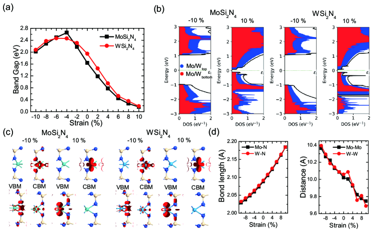
It has been proved that strain engineering is an effective avenue to modulate the electric, magnetic and optical properties of 2D layered materials. To understand the tunability of the energy band gap of the bilayer MoSi2N4 and WSi2N4, we applied biaxial strain to the system. The strain () is evaluated using , where and are the lattice parameter of the strained and unstrained bilayer, respectively. Figure 2(a) shows the evolution of the band gap as a function of applied strain for bilayer MoSi2N4 and WSi2N4. It is suggested that the band gap undergoes a monotonous decreasing with the increasing tensile strain. However, with increasing compress strain, the band gap increases then decreases at around -4 % for the bilayer MoSi2N4 and -6 % for the bilayer MoSi2N4. Besides varying the band gap, more importantly, strain is also found to change an indirect band gap semiconductor to a direct band gap semiconductor at about -4 % of compress strain for the bilayer MoSi2N4.(See Fig. S1) To understand the electronic structure engineering by strain, we draw the projected density of states (PDOS) and partial charge density corresponding to the valance band maximum (VBM) and conduction band minimum (CBM) for bilayer MoSi2N4 and WSi2N4 under -10 % and 10 % strain in Fig. 2(b) and Fig. 2(c). As can be seen from the figure, the VBM and CBM are mostly contributed from both the metal atoms of the top and bottom layer of the bilayer with an enlarged band gap for the compress -10 % strain in the PDOS. In the partial charge density plot, we see more dxy and d orbitals for the metal atoms in VBM and CBM for the compress -10 % strain. This is because the dxy and d orbitals are favorable for the in-plane bonding. The reduced bond length of Mo/W-N under compress strain facilitate the in-plane bonding, as shown in Fig. 2(d). The VBM is mostly from the Mo/W atom of the bottom layer and the CBM is mostly from the Mo/W atom of the top layer, respectively, with a reduced band gap for the tensile 10 % strain. This split of the VBM and CBM from the metal atoms of the two different layer can be understood from the shorten distance of two metal atoms which increases the interlayer interactions as shown in Fig. 2(d). Different from the compressed case, we see more d orbitals for the metal atoms in VBM and CBM for the tensile 10 % strain. This is because the d orbital is favorable for the out-of-plane bonding. When the bond length increase, the out-of-plane bonding become more significant and thus more d orbitals.
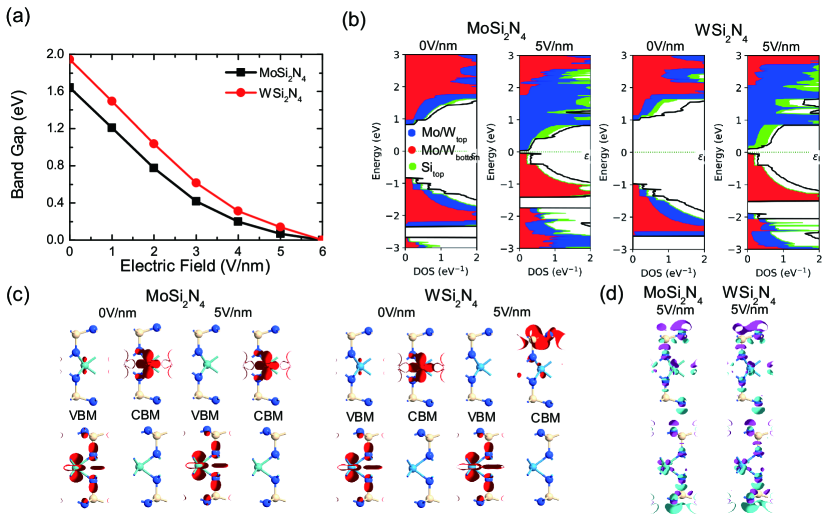
Applying an external electric field perpendicular to the layered material is another effective way of tuning the properties of 2D layered materials. The evolution of the band gap as a function of the applied electric field for bilayer MoSi2N4 and WSi2N4 is provided in Fig. 3(a). It is found that the band gap decreases monotonously with the increasing electric field and closes at 6 V/nm for both bilayer MoSi2N4 and WSi2N4. It is also interesting to find that the CBM for MoSi2N4 is at the K point while the CBM for WSi2N4 moves to the M point when the band gap closes.(See Fig. S2) To gain more insight to the electronic structure engineering by electric field, we plot the PDOS and partial charge density of VBM and CBM for bilayer MoSi2N4 and WSi2N4 under 0 V/nm and 5 V/nm electric field in Fig. 3(b) and Fig. 3(c). As can be seen from the figure, the overall shape of the PDOS of the bottom and top metal atoms almost remain the same under 5V/nm electric field. However, the energy bands of the bottom metal atom shift up while the energy bands of the up atom shift down, which gradually closes the band gap. Furthermore, the CBM of the bilayer WSi2N4 under 5V/nm electric field comes from the top Si atom that can be observed both from the PDOS and the partial charge density plot. This explains why the CBM for WSi2N4 moves to the M point under 5V/nm electric field. This band gap engineering by external electric field can be interpreted from the charge redistribution of the bilayer MoSi2N4 and WSi2N4 under electric field as shown in Fig. 3(d). The charge density difference () is defined as where and are the charge densities of the bilayer MoSi2N4 and WSi2N4 with and without the external electric field, respectively. Here, positive (negative) indicates charge accumulation (depletion). As can be seen from the figure, there is charge accumulation in the bottom layer and depletion in the top layer. This leads to the VBM in the bottom layer shifting up and the CBM in the top layer shifting down, which reduces the energy band gap.
In conclusion, we have shown that the biaxial strain and external electric field are effective ways for the band gap engineering of bilayer MoSi2N4 and WSi2N4. Band gaps can be tuned by both compress and tensile strain. Compress strain can even leads to indirect band gap to direct band gap transition. The change in Mo/W-N bond length and Mo-Mo/W-W distance induced by strain is the main reason for this band structure engineering. Electric field can also modulate the band gap and even semiconductor to metal transition. Charge redistribution induced by the electric field accounts for the band gap tuning. Our study suggests the strain and electric field tunable bilayer MoSi2N4 and WSi2N4 could be promising materials for the next generation nanoelectronics and optoelectronics.
This work is supported by Singapore MOE Tier 2 (Grant No. 2018-T2-1-007). All the calculations were carried out using the computational resources provided by the National Supercomputing Centre (NSCC) Singapore.
Data Availability
The data that support the findings of this study are available from the corresponding author upon reasonable request.
References
- Novoselov et al. (2004) K. S. Novoselov, A. K. Geim, S. V. Morozov, D. Jiang, Y. Zhang, S. V. Dubonos, I. V. Grigorieva, and A. A. Firsov, Science 306, 666 (2004).
- Novoselov et al. (2005a) K. S. Novoselov, D. Jiang, F. Schedin, T. Booth, V. Khotkevich, S. Morozov, and A. K. Geim, Proc. Natl. Acad. Sci. U.S.A. 102, 10451 (2005a).
- Novoselov et al. (2005b) K. S. Novoselov, A. K. Geim, S. V. Morozov, D. Jiang, M. I. Katsnelson, I. V. Grigorieva, S. V. Dubonos, and A. A. Firsov, Nature 438, 197 (2005b).
- Bhimanapati et al. (2015) G. R. Bhimanapati, Z. Lin, V. Meunier, Y. Jung, J. Cha, S. Das, D. Xiao, Y. Son, M. S. Strano, V. R. Cooper, et al., ACS Nano 9, 11509 (2015).
- Tan et al. (2017) C. Tan, X. Cao, X.-J. Wu, Q. He, J. Yang, X. Zhang, J. Chen, W. Zhao, S. Han, G.-H. Nam, et al., Chem. Rev. 117, 6225 (2017).
- Mak et al. (2010) K. F. Mak, C. Lee, J. Hone, J. Shan, and T. F. Heinz, Phys. Rev. Lett. 105, 136805 (2010).
- Radisavljevic et al. (2011) B. Radisavljevic, A. Radenovic, J. Brivio, V. Giacometti, and A. Kis, Nat. Nanotechnol. 6, 147 (2011).
- Splendiani et al. (2010) A. Splendiani, L. Sun, Y. Zhang, T. Li, J. Kim, C.-Y. Chim, G. Galli, and F. Wang, Nano Lett. 10, 1271 (2010).
- Liu et al. (2014) H. Liu, A. T. Neal, Z. Zhu, Z. Luo, X. Xu, D. Tománek, and P. D. Ye, ACS Nano 8, 4033 (2014).
- Li et al. (2014) L. Li, Y. Yu, G. J. Ye, Q. Ge, X. Ou, H. Wu, D. Feng, X. H. Chen, and Y. Zhang, Nat. Nanotechnol. 9, 372 (2014).
- Koenig et al. (2014) S. P. Koenig, R. A. Doganov, H. Schmidt, A. Castro Neto, and B. Özyilmaz, Appl. Phys. Lett. 104, 103106 (2014).
- Qiao et al. (2014) J. Qiao, X. Kong, Z.-X. Hu, F. Yang, and W. Ji, Nat. Commun. 5, 1 (2014).
- Johari and Shenoy (2012) P. Johari and V. B. Shenoy, ACS Nano 6, 5449 (2012).
- Yun et al. (2012) W. S. Yun, S. Han, S. C. Hong, I. G. Kim, and J. Lee, Phys. Rev. B 85, 033305 (2012).
- Bhattacharyya and Singh (2012) S. Bhattacharyya and A. K. Singh, Phys. Rev. B 86, 075454 (2012).
- Pan and Zhang (2012) H. Pan and Y.-W. Zhang, J. Phys. Chem. C 116, 11752 (2012).
- Guo et al. (2014) H. Guo, N. Lu, J. Dai, X. Wu, and X. C. Zeng, J. Phys. Chem. C 118, 14051 (2014).
- Rodin et al. (2014) A. Rodin, A. Carvalho, and A. C. Neto, Phys. Rev. Lett. 112, 176801 (2014).
- Peng et al. (2014) X. Peng, Q. Wei, and A. Copple, Phys. Rev. B 90, 085402 (2014).
- Fei and Yang (2014) R. Fei and L. Yang, Nano Lett. 14, 2884 (2014).
- Ramasubramaniam et al. (2011) A. Ramasubramaniam, D. Naveh, and E. Towe, Phys. Rev. B 84, 205325 (2011).
- Liu et al. (2012) Q. Liu, L. Li, Y. Li, Z. Gao, Z. Chen, and J. Lu, J. Phys. Chem. C 116, 21556 (2012).
- Chu et al. (2015) T. Chu, H. Ilatikhameneh, G. Klimeck, R. Rahman, and Z. Chen, Nano Lett. 15, 8000 (2015).
- Dolui et al. (2012) K. Dolui, C. D. Pemmaraju, and S. Sanvito, ACS Nano 6, 4823 (2012).
- Kou et al. (2012) L. Kou, C. Tang, Y. Zhang, T. Heine, C. Chen, and T. Frauenheim, J. Phys. Chem. Lett. 3, 2934 (2012).
- Liu et al. (2015) Q. Liu, X. Zhang, L. Abdalla, A. Fazzio, and A. Zunger, Nano Lett. 15, 1222 (2015).
- Wu et al. (2015) Q. Wu, L. Shen, M. Yang, Y. Cai, Z. Huang, Y. P. Feng, et al., Phys. Rev. B 92, 035436 (2015).
- Huang et al. (2015) L. Huang, N. Huo, Y. Li, H. Chen, J. Yang, Z. Wei, J. Li, and S.-S. Li, J. Phys. Chem. Lett. 6, 2483 (2015).
- Cao et al. (2019) L. Cao, Y. S. Ang, Q. Wu, and L. Ang, Appl. Phys. Lett. 115, 241601 (2019).
- Hong et al. (2020) Y.-L. Hong, Z. Liu, L. Wang, T. Zhou, W. Ma, C. Xu, S. Feng, L. Chen, M.-L. Chen, D.-M. Sun, et al., Science 369, 670 (2020).
- Novoselov (2020) K. S. Novoselov, Natl. Sci. Rev. 7, 1842 (2020).
- Tang et al. (2020) L. Tang, J. Tan, H. Nong, B. Liu, and H.-M. Cheng, Acc. Mater. Res. (2020).
- Li et al. (2020) S. Li, W. Wu, X. Feng, S. Guan, W. Feng, Y. Yao, and S. A. Yang, Phys. Rev. B 102, 235435 (2020).
- Cao et al. (2021) L. Cao, G. Zhou, Q. Wang, L. Ang, and Y. S. Ang, Appl. Phys. Lett. 118, 013106 (2021).
- Guo et al. (2020a) S.-D. Guo, W.-Q. Mu, Y.-T. Zhu, and X.-Q. Chen, Phys. Chem. Chem. Phys. 22, 28359 (2020a).
- Guo et al. (2020b) S.-D. Guo, Y.-T. Zhu, W.-Q. Mu, and W.-C. Ren, Europhys. Lett. 132, 57002 (2020b).
- Mortazavi et al. (2020) B. Mortazavi, B. Javvaji, F. Shojaei, T. Rabczuk, A. V. Shapeev, and X. Zhuang, Nano Energy 82, 105716 (2020).
- Bafekry et al. (2020) A. Bafekry, M. Faraji, D. M. Hoat, M. Fadlallah, M. Shahrokhi, F. Shojaei, D. Gogova, and M. Ghergherehchi, arXiv:2009.04267 (2020).
- Yang et al. (2020) C. Yang, Z. Song, X. Sun, and J. Lu, arXiv:2010.10764 (2020).
- Yu et al. (2020) J. Yu, J. Zhou, X. Wan, and Q. Li, arXiv:2012.14120 (2020).
- Kang and Lin (2020) L. Kang and Z. Lin, arXiv:2009.06977 (2020).
- Wang et al. (2020) Q. Wang, L. Cao, S.-J. Liang, W. Wu, G. Wang, C. H. Lee, W. L. Ong, H. Y. Yang, L. K. Ang, S. A. Yang, et al., arXiv:2012.07465 (2020).
- Kresse and Furthmüller (1996) G. Kresse and J. Furthmüller, Phys. Rev. B 54, 11169 (1996).
- Kresse and Furthmüller (1996) G. Kresse and J. Furthmüller, Comput. Mater. Sci. 6, 15 (1996).
- Smidstrup et al. (2019) S. Smidstrup, T. Markussen, P. Vancraeyveld, J. Wellendorff, J. Schneider, T. Gunst, B. Verstichel, D. Stradi, P. A. Khomyakov, U. G. Vej-Hansen, et al., J. Phys.: Condens. Matter 32, 015901 (2019).
- Monkhorst and Pack (1976) H. J. Monkhorst and J. D. Pack, Phys. Rev. B 13, 5188 (1976).
- Perdew et al. (1996) J. P. Perdew, K. Burke, and M. Ernzerhof, Phys. Rev. Lett. 77, 3865 (1996).
- Heyd et al. (2003) J. Heyd, G. E. Scuseria, and M. Ernzerhof, J. Chem. Phys. 118, 8207 (2003).
- Grimme et al. (2010) S. Grimme, J. Antony, S. Ehrlich, and H. Krieg, J. Chem. Phys. 132, 154104 (2010).
- Grimme et al. (2011) S. Grimme, S. Ehrlich, and L. Goerigk, J. Comput. Chem. 32, 1456 (2011).
- Wu et al. (2019) Q. Wu, Y. S. Ang, L. Cao, and L. K. Ang, Appl. Phys. Lett. 115, 083105 (2019).